Table of Contents
Advertisement
Quick Links
Download this manual
See also:
Owner's Manual
このサービスマニュアルはエコパルプ
(ECF:無塩素系漂白パルプ)を使用しています。
This document is printed on chlorine free (ECF) paper.
PA
011826
SP2060: 20060720-249900
SERVICE MANUAL
I CONTENTS (目次)
SPECIFICATIONS (総合仕様) ..................................................................... 4
DIMENSIONS (寸法図).............................................................................. 7
PANEL LAYOUT (パネルレイアウト) ......................................................... 8
CIRCUIT BOARD LAYOUT (ユニットレイアウト).................................... 9
DISASSEMBLY PROCEDURES (分解手順) ............................................. 10
LSI PIN DESCRIPTION (LSI端子機能表) .................................................. 17
IC BLOCK DIAGRAM (ICブロック図) ...................................................... 23
CIRCUIT BOARDS (シート基板図) ........................................................... 26
TEST PROGRAM (テストプログラム) ................................................ 36/45
INSPECTIONS (検査) .......................................................................... 54/57
(プログラム、ブート、コンポーネントデータのアップデート)......... 60/64
INITIALIZING (初期化)........................................................................ 68/69
SYSTEM FLOW CHART (電源立ち上げシーケンス).......................... 70/71
DISPLAY MESSAGES (ディスプレイメッセージ)............................. 72/74
OUTPUT LEVEL CHANGE METHOD (出力レベル変更方法) .................. 76
CIRCUIT DIAGRAM (回路図)
Copyright (c) Yamaha Corporation. All rights reserved.
HAMAMATSU, JAPAN
06.06
Advertisement
Table of Contents

Related Manuals for Yamaha SP2060


Summary of Contents for Yamaha SP2060
-
Page 1: Table Of Contents
OUTPUT LEVEL CHANGE METHOD (出力レベル変更方法) ....76 PARTS LIST LEVEL DIAGRAM (レベルダイアグラム) BLOCK DIAGRAM (ブロックダイアグラム) このサービスマニュアルはエコパルプ (ECF:無塩素系漂白パルプ)を使用しています。 WIRING DIAGRAM (基板結線図) This document is printed on chlorine free (ECF) paper. CIRCUIT DIAGRAM (回路図) 011826 SP2060: 20060720-249900 HAMAMATSU, JAPAN Copyright (c) Yamaha Corporation. All rights reserved. 06.06... - Page 2 IMPORTANT NOTICE This manual has been provided for the use of authorized Yamaha Retailers and their service personnel. It has been assumed that basic service procedures inherent to the industry, and more specifically Yamaha Products, are already known and understood by the users, and have therefore not been restated.
- Page 3 SP2060 LITHIUM BATTERY HANDLING This product uses a lithium battery for memory back-up. WARNING : Lithium batteries are dangerous because they can be exploded by improper handling. Observe the following precautions when handling or replacing lithium batteries. • Leave lithium battery replacement to qualified service personnel.
-
Page 4: Specifications (総合仕様
SP2060 SPECIFICATIONS (総合仕様) • General Specifications (一般仕様) • Electrical Characteristics (電気的特性) Output impedance of signal generator: 150 Ω Frequency Response Total Harmonic Distortion * Total Harmonic Distortion is measured with a 18dB/octave filter @80kHz. Hum & Noise * Hum & Noise are measured with a 6dB/octave filter @12.7kHz; equivalent to a 20kHz filter with infinite dB/octave attenuation. - Page 5 SP2060 Crosstalk @1KHz Fs=96kHz * Crosstalk is measured with a 18dB/octave filter @80kHz. LED Level Meters * The LED turns on when the internal limiter is activated. • Input/Output Characteristics (入出力特性) Analog Input Characteristics *1. XLR-3-31 type connectors with latches are balanced. (1=GND, 2=HOT, 3=COLD) *2.
- Page 6 SP2060 Control I/O Characteristics • Connector Pin Assignment (コネクターピンアサイン) [NETWORK] Connector (100Base-TX Ethernet, RJ-45) [NETWORK] 端子 (100Base-TX Ethernet、RJ-45コネクター)...
-
Page 7: Dimensions (寸法図
SP2060 DIMENSIONS (寸法図) Unit: mm 単位:mm... -
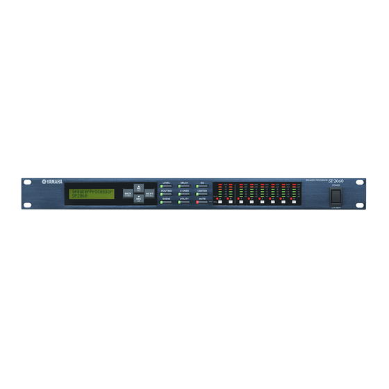
Page 8: Panel Layout (パネルレイアウト
SP2060 PANEL LAYOUT (パネルレイアウト) • Front Panel (フロントパネル) STORE RECALL 8 A 9 B 0 1 Display 1 ディスプレイ 2 [BACK/STORE] Key 2 [BACK/STORE] キー 3 [LINC/YES]/[MDEC/NO] Keys 3 [▲INC/YES] / [ ▼DEC/NO] キー 4 [NEXT/RECALL] Key 4 [NEXT/RECALL] キー... -
Page 9: Circuit Board Layout (ユニットレイアウト
SP2060 CIRCUIT BOARD LAYOUT (ユニットレイアウト) POWER SUPPLY UNIT LCD MODULE... -
Page 10: Disassembly Procedures (分解手順
SP2060 I DISASSEMBLY PROCEDURES (分解手順) ラックアングル (所要時間:約1分) Rack Angle (Time required: About 1 min.) 1-1. Remove the three (3) screws marked [1050]. The rack 1-1. [1050] のネジ3本を外し、ラックアングルLを外しま angle L can then be removed. (Fig. 1) す。 (図1) 1-2. Remove the three (3) screws marked [1020]. The rack 1-2. - Page 11 SP2060 フロントパネル (所要時間:約3分) Front Panel (Time required: About 3 min.) 3-1. Remove the rack angle L and R. (See procedure 1) 3-1. ラックアングルL、Rを外します。 (1項参照) 3-2. Remove the top cover. (See procedure 2) 3-2. トップカバーを外します。 (2項参照) 3-4. Remove the screw marked [940] and three (3) screws 3-3.
- Page 12 SP2060 ANAシート (所要時間:約5分) ANA Circuit Board (Time required: About 5 minutes.) 4-1. ラックアングルL、Rを外します。 (1項参照) 4-1. Remove the rack angle L and R. (See procedure 1) 4-2. トップカバーを外します。 (2項参照) 4-2. Remove the top cover. (See procedure 2) 4-3. [240] のネジ6本、 [250] のネジ12本、 [260] のネジ4本を...
- Page 13 SP2060 Rear view [140] [500] [240] [250] [240] [250] [240] [140]: Bind Head Tapping Screw-B 3x8 MFZN2B3 (WE774400) Bタイト+BIND Bind Head Tapping Screw-B 3x8 MFZN2B3 (WE774400) Bタイト+BIND [240]: [250]: Bind Head Tapping Screw-B 3x8 MFZN2B3 (WE774400) Bタイト+BIND Bind Head Tapping Screw-S 3x6 MFZN2B3 (WE877800) Sタイト+BIND [500]: (Fig.
- Page 14 SP2060 CPUシート (所要時間:約4分) CPU Circuit Board (Time required : About 4 minutes.) 9-1. ラックアングルL、Rを外します。 (1項参照) 9-1. Remove the rack angle L and R. (See procedure 1) 9-2. トップカバーを外します。 (2項参照) 9-2. Remove the top cover. (See procedure 2) 9-3. [70] のネジ4本を外し、CPUシートを外します。 (図5)...
- Page 15 SP2060 [30] [70] [40] [40] ● Lithium Battery(リチウム電池) Battery VN103500 VN103600(Battery holder for VN103500) Notice for back-up battery removal Push the battery as shown in figure, then the battery will pop up. Druk de batterij naar beneden zoals aangeven in de tekening, de batterij springt dan naar voren.
- Page 16 SP2060 液晶ディスプレイ (所要時間:約4分) LCD Module (Time required : About 4 minutes.) 12-1. ラックアングルL、Rを外します。 (1項参照) 12-1. Remove the rack angle L and R. (See procedure 1) 12-2. トップカバーを外します。 (2項参照) 12-2. Remove the top cover. (See procedure 2) 12-3. フロントパネルを外します。 (3項参照) 12-3. Remove the front panel. (See procedure 3) 12-4.
-
Page 17: Lsi Pin Description (Lsi端子機能表
SP2060 LSI PIN DESCRIPTION (LSI端子機能表) CONTENTS (目次) • AK4393-VF-E2 (XW029A00) DAC (Digital to Analog Converter) ..17 • AK5385BVF-E2 (X5364B00) ADC (Analog to Digital Converter) ..17 • HD6417727F160CV (X2890B00) CPU (Microprocessor 32 bit) .... 18 • YSS919B-HZ (XZ693B00) DSP7 (Digital Signal Processor) ....20 •... - Page 18 SP2060 • HD6417727F160CV (X2890B00) CPU (Microprocessor 32 bit) CPU: IC002 Name Function Name Function Vcc-RTC Power supply for RTC (1.9V) VccQ VccQ XTAL2 Not in use (XTAL for internal RTC) EXTAL2 Vss-RTC Power supply for RTC (0V) ...
- Page 19 SP2060 CPU: IC002 Name Function Name Function Reserved//CAS/PTJ[2] CAS for SDRAM STATUS1/PTJ[7] Output port (Flash ROM ACC) VssQ VssQ CL2/PTH[7] LCD clock output Reserved/PTJ[3] Output port (DAC Reset) VssQ VssQ VccQ VccQ CKIO System clock input/output (for SDRAM) Reserved/PTJ[4] Output port (SIO Reset)
- Page 20 SP2060 • YSS919B-HZ (XZ693B00) DSP7 (Digital Signal Processor) DSP: IC153 Name Function Name Function PLLEN PLL enable input (0: PLL unuse, 1: PLL use) Ground /TEST Test mode setting (0: TEST, 1: Normal) CD07 AVss Analog ground CD06 ...
- Page 21 SP2060 DSP: IC153 Name Function Name Function SIO32 DA11 SIO33 DA12 SIO34 DA13 Memory data bus SIO35 DA14 Serial data bus SIO36 DA15 SIO37 Ground SIO38 Power supply (3.3 V) ...
- Page 22 SP2060 • KSZ872ISL (X5621A00) PHYceiver ENT: IC109 Name Function Name Function MDIO Management Independent Interface (MII) INT#/PHYAD0 Ipd/O Management Interface (MII) Interrupt Out. Data I/O. LED0/TEST Ipd/O Link/Activity LED Output. MII Clock Input. LED1/SPD100/noFEF Ipd/O Speed LED Output. RXD3/PHYAD...
-
Page 23: Ic Block Diagram (Icブロック図
SP2060 IC BLOCK DIAGRAM (IC ブロック図) • 74VHC245MTCX_NF40 (X0296A00) • NJM2068M-D (TE2) (X3505A00) • NJM2904V (TE1) (XR532A00) Bus Tranciever Operational Amplifier Operational Amplifier CPU: IC003 ANA: IC401, 402 CPU: IC010 +DC Voltage +DC Voltage Output A Output A Supply Supply... - Page 24 SP2060 • SN74LV00APWR (X4460A00) • SN74LV04APWR (X5965A00) • SN74LV08APWR (X4463A00) Quad 2 Input Positive NAND Gate Inverter Quad 2 Input AND DSP: IC050 DSP: IC003, 018, 053, 257 DSP: IC051 • SN74LV11APWR (X3516A00) • SN74LV21APWR (X2377A00) • SN74LV244APWR (X3292A00) Triple 3 Input AND...
- Page 25 SP2060 • SN74LVCC4245APWR (X3096A00) • TC7SH04FU (XS775A00) • TC7SH08FU (XR680A00) Dual Supply Octal Bus Transceiver Inverter 2 Input AND Gate DSP: IC251 ENT: IC110 ENT: IC114 VCCA VCCB IN B VCCB IN A OUT Y • TC7SH32FU (XW633A00) • TC7WH04FU (XY363A00) •...
-
Page 26: Circuit Boards (シート基板図
SP2060 CIRCUIT BOARDS (シート基板図) CONTENTS (目次) • PS Circuit Board (X7297C0) ..........26 • PN Circuit Board (X7297C0) ..........27 • ANA Circuit Board (X7298C0) ..........28 • CPU Circuit Board (X6028C0) ..........30 • ENT Circuit Board (X7295C0) ..........31 •... - Page 27 SP2060 • PN Circuit Board LEVEL DELAY BACK NEXT ROUTING X-OVER LIMITER SCENE UTILITY MUTE OVER OVER LIMIT Component side (部品側) Pattern side (パターン側) 2NA-WG30340...
- Page 28 SP2060 • ANA Circuit Board Not used to DSP- CN450 2NA-WG30400 Component side (部品側)...
- Page 29 SP2060 • ANA Circuit Board 2NA-WG30400 Pattern side (パターン側)...
- Page 30 SP2060 • CPU Circuit Board Component side (部品側) to DSP- CN001 Pattern side (パターン側) 2NA-WG30150...
- Page 31 SP2060 • ENT Circuit Board Not used Component side (部品側) Pattern side (パターン側) 2NA-WG30200...
- Page 32 SP2060 • DSP Circuit Board to LCD to ANA_CN701 to PN- CN201 Component side (部品側) 2NA-WG30170...
- Page 33 SP2060 • DSP Circuit Board Pattern side (パターン側) 2NA-WG30170...
- Page 34 SP2060 • DC Circuit Board to DSP- CN310 Component side (部品側) 2NA-WG30340...
- Page 35 SP2060 • DC Circuit Board Pattern side (パターン側) 2NA-WG30340...
-
Page 36: Test Program (テストプログラム
Version Number 2 Double click on “copy_sp2060.bat”. Then the all files of the SP2060 data package are copied to C:¥TOOLS_SP2060 automatically. The files are overwritten even when the C:¥TOOLS_SP2060 folder is already made and the files are in it. - Page 37 1-3. Connection Connect the NETWORK connector of the SP2060 to the LAN connector of the personal computer with the LAN cross cable. Connect the DIGITAL OUTPUT connector of the equipment with digital out (AES/EBU), for example SPX2000, to the DIGITAL INPUT connector of SP2060 with the XLR (AES/EBU) cable.
- Page 38 SP2060 Press the [ ↓ ] and [ ↑ ] keys of the personal computer to move “*” mark at the position of “01 Product-SP2060”, and press the [0] 2-4. (zero) key. (The manual mode is selected.) Then the testing item selection list screen is displayed.
- Page 39 SP2060 Outline of Tests 3-1. SRAM Test (NO. 01) Content: Checks Address Bus and Data Bus of SRAM. Example of execution screen *** 01. SRAM *** SRAM AddressBus Displayed at OK SRAM DataBus EXIT:[ENTER] *** 01. SRAM *** SRAM AddressBus ...
- Page 40 SP2060 3-3. PLLP2 Test (NO. 03) Content: Compares and checks registers (00h, 0Fh, 10h, 16h) of the PLLP2 by writing and reading them. Example of execution screen *** 03. PLLP2 *** 0x00 W/R OK! Displayed at OK 0x0F W/R OK! ...
- Page 41 SP2060 (2) Display Screen at NG *** 04. DSP7 *** DSP7 CPUIF DATABUS--- CHIP #0 OK! DSP7 CPUIF ADRBUS--- CHIP #0 OK! DSP7 CPUIF CHIPSEL--- CHIP #0 OK! DSP7 ERAMIF DATABUS--- CHIP #0 NG! DSP7-1 ffffffff DSP7 ERAMIF ADRBUS--- CHIP #0 NG!
- Page 42 SP2060 3-6. LCD Test (NO. 13) Content: Check visually if entire LCD displays black and white repeatedly. Example of execution screen *** 13. LCD *** OK:[ENTER],NG:[0] 1 Make sure that all the screen is shown in black and white. The reversing cycle shifts the display every second repeating it for five seconds.
- Page 43 Checks the lock condition, word clock frequency and channel status automatically, and the the rusult is displayed. At this time, 46 kHz audio data input to DIGITAL INPUT connector is output to OUTPUT 1, 2. 3 Next, disconnect the XLR cable from DIGITAL INPUT connector of SP2060, and then press [ENTER] key of the personal computer.
- Page 44 SP2060 3-10. ANALOG Test (NO. 20) Content: Checks the operation of ANALOG MUTE. Example of execution screen *** 20. ANALOG MUTE *** MUTE=OFF OK:[ENTER],NG:[0] MUTE=ON OK:[ENTER],NG:[0] 1 In this mode, ANALOG OUT is in MUTE OFF condition. Check that the audio signal is out put.
- Page 45 既にC:¥TOOLS_SP2060フォルダがあり、その中にファイルがあっても上書きされます。 ③ TeraTermのインストール ¥driver¥TeraTermにある “setup.exe” をダブルクリックします。 するとTera Term Pro Setup 画面が表示されます。 これ以降は画面の指示にしたがって操作して、インストールを完了してください。 ④ DME-N Network Driverのインストール ¥driver¥DME-N Network Driver¥DME-N Network Driver Vx.xxにある “setup.exe” をダブルクリックします。 するとYAMAHA DME-N Network Driver-InstallShield Wizard が起動します。 これ以降は画面の指示にしたがって操作して、インストールを完了してください。 ⑤ Ethernet設定 (コントロールパネル→ネットワーク接続→ローカルエリア接続→プロパティ→TCP/IPプロパティ:Win Xpの場合) IP アドレス 192.168.0.1 サブネットマスク 255.255.255.0 ⑥...
- Page 46 DIGITAL INPUT (AES/EBU) Digital LANケーブル (クロス) DIGITAL OUTPUT (AES/EBU) SPX2000など SP2060接続図 操作 2-1. SP2060の [UTILITY] と [NEXT/RECALL] キーを押しながら電源をONし、 [UTILITY] と [NEXT/RECALL] キーを押しつづけ ます。 するとテストプログラムが起動し、約10秒後、イーサネット通信可能状態になると [LEVEL] LEDが点灯します。 [NEXT/RECALL] [LEVEL] LED [UTILITY] 2-2. C:¥TOOLS_SP2060¥tools¥TeraTerm-Settingにある “diag_start” をクリックします。 するとTeraTermが起動します。 2-3. パソコンの画面に “Press [ ENTER] ” と表示されたらパソコンの [ENTER] キーを押します。...
- Page 47 SP2060 2-4. パソコンの [↓] [ ↑] キーで “*” マークを “01 Product-SP2060” の位置に移動し、 [0] ( ゼロ) キーを押します。 (MANUALモード を選択) すると検査項目選択リスト画面が表示されます。 検査項目選択リスト画面例 ** Diag Mode ** Total Result [ ] * 00 RESERVE-SP2060 01 SRAM 検査結果 02 BATTERY 03 PLLP2...
- Page 48 SP2060 各検査項目の説明 3-1. SRAM検査 (NO. 01) 内容: SRAM のAddress Bus、Data Busを検査します。 実行画面例 *** 01. SRAM *** SRAM AddressBus OKの場合に表示 SRAM DataBus EXIT:[ENTER] *** 01. SRAM *** SRAM AddressBus NGの場合に表示 SRAM DataBus EXIT:[ENTER] メッセージ ・ アドレスバスアクセス異常検出時:...
- Page 49 SP2060 3-3. PLLP2検査 (NO. 03) 内容: PLLP2 のレジスタ (00h、0Fh、10h、16h) をWrite/Readして比較し判定します。 実行画面例 *** 03. PLLP2 *** 0x00 W/R OK! OKの場合に表示 0x0F W/R OK! 0x10 W/R OK! NGの場合に表示 0x16 W/R 0x16 W:0x0F R:0x00 EXIT:[ENTER] トラブルシューティング NGの場合は以下の部分をチェック。 PLLP2 ( DSPシート:IC052) の不良、PLLP2とCPU (CPUシート:IC002) 間に接続されている信号線 (アドレスバス・デー...
- Page 50 SP2060 (2) NG時表示画面 *** 04. DSP7 *** DSP7 CPUIF DATABUS--- CHIP #0 OK! DSP7 CPUIF ADRBUS--- CHIP #0 OK! DSP7 CPUIF CHIPSEL--- CHIP #0 OK! DSP7 ERAMIF DATABUS--- CHIP #0 NG! DSP7-1 ffffffff DSP7 ERAMIF ADRBUS--- CHIP #0 NG! DSP7-1 0000000f ...THE END OF DIAGNOSTICS...
- Page 51 SP2060 3-6. LCD検査 (NO. 13) 内容: LCDの画面全体を黒と白の繰り返し表示にし、目視判定します。 実行画面例 *** 13. LCD *** OK:[ENTER],NG:[0] ① 全画面が黒・白表示されることを確認します。 反転表示周期は1秒周期で切り替え表示し、5秒間繰り返します。 ② 全画面にドットの欠けがないことを確認します。 トラブルシューティング NGの場合はDSPシート:CN270を経由する信号を確認してください。 又はLCDモジュールの不良。 3-7. LED検査 (NO. 14) 内容: パネルのLEDが規定の順序で点灯することを目視判定します 実行画面例 *** 14. LED *** OK:[ENTER],NG:[0] ① 点灯順序はパネル左側より右側方向へ順次点灯させます。 ② 全LEDの点灯が完了した時点で、全点灯させてテスト終了とします。 (全点灯はLEDの明るさを確認する為) トラブルシューティング NGの場合はDSPシート:CN250を経由する信号を確認してください。...
- Page 52 SP2060 トラブルシューティング NGの場合はDSPシート:CN250を経由する信号を確認してください。 又はスイッチの個別不良。 注意 ・ 検査順序はパネル左端より順番に右側方向のキー名称を表示し、表示されているキーを押します。 ・ ここではキーの精度を検査目的としているので、LED付きキーを押しても該当LEDは点灯しません。 3-9. DIGITAL IN検査 (NO. 17) 内容: DIGITAL INに96 KHz/48 KHzの信号を入力し、DIRの動作を確認します。 LOCK、FS、チャネルステータスを確認する事により動作を確認します。 実行画面例 ** 17. DIGITAL IN *** 96KHz OK. Change 48KHz [ENTER] 48KHz OK. AES/EBU Cable Release [ENTER] Release OK. EXIT:[ENTER] ①...
- Page 53 SP2060 3-10. ANALOG検査 (NO. 20) 内容: ANALOG MUTE の動作を確認します。 実行画面例 *** 20. ANALOG MUTE *** MUTE=OFF OK:[ENTER],NG:[0] MUTE=ON OK:[ENTER],NG:[0] ① このテストモードに入るとANALOG OUTがMUTE OFF状態になります。 音が出ることを確認します。 音が出ている場合、 [ENTER] キーを押します。 音が出ていない場合、 [0] キーを押します。 ② [ENTER] が押されるとMUTE ON状態になります。 音が出なくなることを確認します。 音が出ていない場合、 [ENTER] キーを押します。 音が出ている場合、 [0] キーを押します。...
-
Page 54: Inspections (検査
SP2060 INSPECTIONS Measurement Conditions 1-1. Environment • Normal temperature: 5 to 40 degree • Normal humidity: 30 to 90 % 1-2. Power Source The voltage is within ±10 %. • U : 120 V • H : 230 V • B : 230 V •... - Page 55 SP2060 3 Noise level Terminate the INPUT A, B terminals with the resistances of 150 Ω and then measure the output level obtained at OUTPUT 1~6 terminals. Variation width -79 dBu or less 4 Level difference among OUTPUT 1~6 terminals The range of difference in the gain measured in 1 is specified as follows.
- Page 56 SP2060 1 Gain Input frequency Input level Specified output level Variation width 1 kHz -20 dBFS +4 dBu +4±1 dBu 2 Frequency Characteristics Measure the each frequency response compared with the 1 kHz (0 dB). Input frequency Input level Output level (reference)
- Page 57 SP2060 検査 測定条件 1-1. 環境 ・ 常温:5∼40 ℃ ・ 常湿:30∼90 % 1-2. 電源電圧 電源電圧 (AC100V) の±10 %で測定すること。 ANALOG特性検査 ANALOG特性検査は、テストプログラムを使用して測定します。 2-1. 準備 テストプログラムの 「1. 準備」 ( 45∼46ページ) を参照してください。 2-2. 測定条件 特に指定の無い場合、以下の条件とします。 ・ 0 dBu=0.775 Vrmsとします。 ・ 0 dBFS=0 dBデジタルフルスケールとします。 ・ アナログ出力の負荷抵抗は各チャンネルとも600 Ωとします。...
- Page 58 SP2060 ③ ノイズレベル INPUT A、B端子を150 Ωで終端します。 OUTPUT 1∼6端子のノイズレベルを測定します。 許容範囲 -79 dBu 以下 ④ CH間レベル差 ①で測定したOUTPUT 1∼6間の利得の差の範囲を以下のように規定します。 許容範囲 1 dB 以内 ⑤ A−Bチャンネル間クロストーク ⑤-1 チャンネルAからチャンネルBへのクロストーク INPUT B端子を150 Ωで終端します。 INPUT A端子に下記の信号を入力し、OUTPUT 1、3、5 ( 奇数チャンネル) 端子とOUTPUT 2、4、6 ( 偶数チャンネル) 端子の出力レベルを測定します。 出力レベル 許容範囲 入力周波数...
- Page 59 SP2060 ① 利得 入力周波数 入力レベル 規定出力レベル 許容範囲 1 kHz -20 dBFS +4 dBu +4±1 dBu ② 周波数特性 測定方法…1 kHzを基準として、各入力周波数における相対値を測定します。 入力周波数 入力レベル 出力レベル (参考値) 20 Hz -20 dBFS +4 dBu -1.0∼+0.5 dB 40 kHz -20 dBFS +4 dBu -1.0∼+0.5 dB ③ 全高調波歪率...
-
Page 60: Updating Program, Boot And Component Data
Refer to “Test program 1-2. Personal Computer Setting” on page 36 for information on setting the personal computer. 1-3. Connection Connect the NETWORK connector of the SP2060 to the LAN connector of the personal computer with the LAN cross cable. Updating the program and boot 2-1. - Page 61 Updating Click on “Connect...”. When “Connection succeeded.” is displayed, click on “Update Firmware...”. (Fig. 2 [Checking connection screen]) When “Firmware update completed.” is displayed and then SP2060 is restarted, updating is end. (Fig. 3 [Update completed screen]) Note Never turn off the power to the SP 2060 until the updating is completed.
- Page 62 2-5. Solution when error message is displayed • When the error message as shown below is displayed, stop updating software, turn off the power to the SP2060, and then follow from step “2-1. Activating the SP2060”. • Same message is still displayed, restart the personal computer, turn off the power to the SP2060, and then follow from step “2-1.
- Page 63 Operation 1 While pressing the [SEL5] and [SEL6] keys, turn on the power to the SP2060. Keep pressing the [SEL5] and [SEL6] keys until “Copyright 2006 YAMAHA” disappears from the display of SP2060. 2 Double click on “sync.exe” of C:¥TOOLS_SP2060¥tools¥sync¥component¥.
-
Page 64: プログラム、ブート、コンポーネントデータのアップデート
:1台 1-2. パソコンの設定 「テストプログラム1-2 パソコンの設定」 ( 45ページ) にしたがってパソコンを設定します。 1-3. 接続 SP2060のNETWORK端子とパソコンのLAN端子をLANケーブル (クロス) で接続します。 プログラムとブートのアップデート 2-1. 本体の起動 [SEL5] と [SEL6] キーを押しながらSP2060の電源をONし、 “Copyright 2006 YAMAHA” がSP2060の表示画面から消えるまで [SEL5] と [SEL6] キーを押しつづけます。 [POWER] [SEL5] [SEL6] 2-2. アップデートソフトの起動 プログラム部とブート部で起動方法が異なります。 ・ プログラム部をアップデートする場合 C:¥TOOLS_SP2060¥tools¥update¥prog¥にある 「update.exe」 をクリックします。 ・ ブート部をアップデートする場合... - Page 65 SP2060 図1 設定・実行画面 2-4. アップデート 「接続」 をクリックします。 「接続チェック終了。」 と表示されたことを確認して、 「更新」 をクリックします。 (図2 [ 接続チェック終了画面] 参照) 「更新成功しました。」 と表示され、SP2060 が再起動すれば、アップデート終了となります。 (図3 [ アップデート完了画面] 参照) 注意 アップデートが完了するまでSP2060の電源は切らないでください。 図2 接続チェック終了画面 図3 アップデート完了画面...
- Page 66 SP2060 2-5. エラーメッセージが出たときの処理 ・ 以下のようなエラーメッセージが表示された場合は、アップデートソフトを終了し、SP2060の電源をOFFし、2-1からや り直してください。 ・ それでも同じメッセージが続く場合は、PCを再起動し、SP2060の電源をOFFし、2-1からやり直してください。 エラーメッセージ一覧 [エラー] デバイスに接続できませんでした。 [エラー] 通信ポートの確保に失敗しました。 [エラー] プロダクト名を取得できませんでした。 [エラー] SysEx用のメモリが足りません。 [エラー] ファイルが開けません。 [エラー] 異なるファイルです。 [エラー] メモリが足りません。 [エラー] ファイルが読めません。 [エラー] 通信制御権の取得に失敗しました。 [エラー] コマンドパケットのサイズの取得に失敗しました。 [エラー] コマンドパケットの作成用のメモリが足りません。 [エラー] コマンドパケットの作成に失敗しました。 プログラムとブートのバージョン確認 プログラムとブートのバージョンを確認するには2つの方法があります。 3-1. テストプログラムによる方法 テストプログラムを起動したときに表示される検査カテゴリ選択リスト画面にプログラムとブートのバージョンが表示され ます。 詳しくは46ページの 「テストプログラム 2. 操作」 を参照してください。...
- Page 67 注意 ただし最新のブート部のダウンロードはできません。 最新のブート部が必要な場合、YSISSホームページからSP2060データパッケージをダウンロードしてください。 コンポーネントデータのアップデート プログラムまたはブートをアップデートした場合、必ずコンポーネントデータのアップデートを実施してください。 コンポーネントデータのアップデートを実施しなかった場合、初期化 (FACTORY SETUPなど) の時にエラーメッセージが表 示される場合があります。 5-1. 操作 1 [SEL5] と [SEL6] キーを押しながらSP2060の電源をONし、 “Copyright 2006 YAMAHA” がSP2060の表示画面から消えるま で [SEL5] と [SEL6] キーを押しつづけます。 2 C:¥TOOLS_SP2060¥tools¥sync¥component¥にある 「sync.exe」 をダブルクリックします。 するとアップデートソフトが起動し、設定・実行画面が表示されます。 3 画面上のパラメータを下記のように設定します。 出力ポート :ZONE1 入力ポート :ZONE1 ターゲットID :2 実行ファイル...
-
Page 68: Initializing (初期化
5. Press the [INC/YES] key to start initialization operation. During initialization, the following message appears. Executing.. When you press the [DEC/NO], initialization is canceled. 6. When initialization is completed, the SP2060 displays the following message, then automatically restarts. Completed! [BACK/STORE] [ INC/YES] [POWER]... - Page 69 FACTORY SETUP 工場出荷時の状態に戻す 初期化 初期化 消去 注意 バッテリーによりバックアップされているデータは、シーン番号とカレントシーンです。 [SRAM (CPUシート:IC009) ] 内蔵メモリーを初期化すると、それまでメモリー内に保存されていた内容が失われます。 初期化の前に、DME Designerのバックアップ機能を使って、データをパソコンなどの外部機器に保存してください。 その操作方法の詳細は、DME Designer取扱説明書を参照してください。 以下の操作は慎重に行なってください。 1. SP2060の電源をオフにします。 2. [BACK/STORE]キーを押しながら電源をオンにし、初期化画面が表示されるまで[BACK/STORE]キーを押し続けます。 INITIALIZE CURRENT BACKUP 3. [INC]/[DEC]キーで初期化方法を選択します。 注意 初期化をキャンセルする場合には、 “Exit” を選択して確定するか、そのまま電源を入れ直してください。 4. [NEXT]キーでカーソルを に移動し、[INC/YES]を押します。 すると下記のメッセージが表示されます。 INITIALIZE ARE YOU SURE? 5. [INC/YES]キーを押すと、初期化が開始されます。...
-
Page 70: System Flow Chart (電源立ち上げシーケンス
SYSTEM FLOW CHART Purpose SP2060 is provided with the test program for diagnosing the hardware. However, when the test program can not be activated, the troubleshooting is hard. The system flow chart shows the software’s action flow after releasing reset and may help you to troubleshoot. - Page 71 外部デバイス初期 FLASH ROM動作 初期画面表示 化前にHに変更 不良、SDRAM動 作不良 タスク動作開始後 外部デバイスの不 にLに変更 良 (その後LCD初期 LCD初期画面 画面表示) Speaker Processor H<->L 500msec毎にH/L YAMAHA SP2060 切り替え出力 [UTILITY] + [ NEXT] テストプログラム キー押下チェック モード サムエラー Download Program部のサムチェック モード (プログラムの破損確認) Program部起動 LCD Copyright表示 内部・外部デバイス再初期化と Copyright 2006 画面表示...
-
Page 72: Display Messages (ディスプレイメッセージ
Activate the test program, and then check the defect. (such as Try again! output is muted. SRAM and BATTERY) * Do NOT turn off the power to the SP2060 while the unit displays the message “DO NOT TURN OFF!” at the bottom of the display. - Page 73 Deleting a scene. Do NOT turn power off while the unit displays this message. * Do NOT turn off the power to the SP2060 while the unit displays the message “DO NOT TURN OFF!” at the bottom of the display.
- Page 74 SP2060 ディスプレイメッセージ • ワーニング/エラーメッセージ メッセージ 内容 対策 Duplicate IP Adr. IPアドレスが重複しています。 IPアドレスを重複しないように設定しなおしてください。 Illegal MAC Adr. 無効なMACアドレスが設定されています。 機器の故障と思われます。CPUシートを交換してください。 Invalid IP Adr. IPアドレスが正しくありません。 正しいIPアドレスを設定してください。 ケーブルが抜けていたり、接続しているハブやルー ケーブルを正しく接続し、ハブやルーターなどの機器を正常 Network Error ターの電源が切れていたり、もしくはケーブルが不 に動作させてください。 適切な状態にある可能性があります。 No MAC Adr. MACアドレスが設定されていません。 機器の故障と思われます。CPUシートを交換してください。 電源をオフにすると現在の設定が失われ、初期値に戻ります。 バッテリーが完全に消耗している、もしくは装着 No Battery バッテリーを交換してください。その後FACTORY SETUPを...
- Page 75 SP2060 • ステータスメッセージ メッセージ 内容 Connecting ネットワークを接続中です。 Download Success プログラムの更新に成功しました。 Downloading プログラムを更新しています。メッセージ表示中は電源を切らないでください。 コンピューターからシーンに関する情報を操作しています。メッセージ表示中は電源を切らないでくださ File Operating い。 Network Setup ネットワーク接続の準備中です。 Panel Locked ユーザーロックが設定されています。パネル操作できません。 Panel Unlocked ユーザーロックが解除されました。パネル操作できます。 Scene Recalling シーンリコール中です。 Scene Storing シーンストア中です。メッセージ表示中は電源を切らないでください。 Cannot Recall シーンやライブラリーのリコールが禁止されています。 Cannot Store シーンストアが禁止されています。 NO X-OVER X-OVERはインプットチャンネルのパラメーターにはありません。...
-
Page 76: Output Level Change Method (出力レベル変更方法
SP2060 OUTPUT LEVEL CHANGE METHOD (出力レベル変更方法) The maximum output level obtained at OUTPUT 1~6 ter- 工場出荷時、OUTPUT 1∼6の最大出力レベルは+24 dBuに minals is +24 dBu when the SP2060 is shipped out from 設定されていますが、+24 dBuから+18 dBuへの変更をユー the factory. ザーが希望された場合、下記に従ってANAシートの部品を When the customer required to change the maximum out- 交換してください。... - Page 77 SP2060 R306 C312 R308 R312 R314 R313 R315 R309 C313 R307 R206 C212 R208 R212 R214 R213 R215 R209 C213 R207 R106 C112 R108 R112 R114 R113 R115 R109 C113 R107...
- Page 78 SP2060 Inspection after exchanging the components 部品交換後の検査 Input analog signal to INPUT A, B terminals and then mea- INPUT A、B端子にアナログ信号を入力し、OUTPUT 1∼ sure the output signal obtained at OUTPUT 1~6 terminals. 6端子の出力信号を測定します。 For the details of the measuring procedures, refer to IN- 測定手順の詳細は...
-
Page 79: Parts List
SP2060 PARTS LIST I CONTENTS (目次) OVERALL ASSEMBLY (総組立) ............3 ELECTRICAL PARTS (電気部品) ............7 Notes: DESTINATION ABBREVIATIONS Australian model South African model British model Chinese model Canadian model South-east Asia model German model Taiwan model European model U.S.A. model... - Page 80 SP2060 OVERALL ASSEMBLY 1/2 (総組立 1/2) 1090 1050 1030 ±0.15 (0.2) 560b 1020 1000 560c The inlet assembly consists of the AC inlet, ferrite core, 560c to 560b Details of putting cables and other things. 560c と 560b の貼り合せ詳細図 560e...
- Page 81 SP2060 OVERALL ASSEMBLY 2/2 (総組立 2/2) Fix the connector assembly with the cord holder. インシュロックタイで 束線を固定 Bond the capacitor with the adhensive. 接着剤で Put the cushion FFC around on upper and lower face of コンデンサを固定 bending part of the flexible flat cable as shown in Fig. above.
- Page 82 SP2060 PART NO. DESCRIPTION 部 品 名 REMARKS REF NO. RANK OVERALL ASSEMBLY 総 組 立 SP2060 (WG20180) WG359700 Bottom Chassis ボ ト ム シ ャ ー シ 印 刷 品 WE877800 Bind Head Tapping Screw-S MFZN2B3 S タ イ ト + B I N D...
- Page 83 SP2060 PART NO. DESCRIPTION 部 品 名 REMARKS REF NO. RANK 1080 WB426600 Button PSW ボ タ ン P S W POWER ON/OFF 1090 Label, Name Plate ラ ベ ル (WG50280) ACCESSORIES 付 属 品 VT119800 AC Cord J 7A 125V 3P 2.5m 電...
- Page 84 SP2060 ELECTRICAL PARTS (電気部品) PART NO. DESCRIPTION 部 品 名 REMARKS REF NO. RANK ELECTRICAL PARTS 電 気 部 品 SP2060 WG304000 Circuit Board A N A シ ー ト (X7298C0) WG301500 Circuit Board C P U シ ー ト...
- Page 85 SP2060 PART NO. DESCRIPTION 部 品 名 REMARKS REF NO. RANK C236 US061330 Ceramic Capacitor-CH(chip) 33pF 50V J チ ッ プ セ ラ( C H ) C237 US061330 Ceramic Capacitor-CH(chip) 33pF 50V J チ ッ プ セ ラ( C H )...
- Page 86 SP2060 PART NO. DESCRIPTION 部 品 名 REMARKS REF NO. RANK C514 UU238100 Electrolytic Cap. 100uF 16V ケ ミ コ ン F W C516 UU238100 Electrolytic Cap. 100uF 16V ケ ミ コ ン F W C517 US064100 Ceramic Capacitor-B (chip) 0.01uF 50V K...
- Page 87 SP2060 PART NO. DESCRIPTION 部 品 名 REMARKS REF NO. RANK -804 WA093400 LC Filter ZJSR5101-223TA-01 L C フ ィ ル タ ー E M I EM806 WA093400 LC Filter ZJSR5101-223TA-01 L C フ ィ ル タ ー E M I...
- Page 88 SP2060 PART NO. DESCRIPTION 部 品 名 REMARKS REF NO. RANK R138 V I 1 9 7 4 0 0 Metal Film Resistor (chip) 10K 1/10W D チ ッ プ 金 被 抵 抗 -141 V I 1 9 7 4 0 0...
- Page 89 SP2060 PART NO. DESCRIPTION 部 品 名 REMARKS REF NO. RANK R310 V I 1 9 7 0 0 0 Metal Film Resistor(chip) 6.8K 1/10W D チ ッ プ 金 被 抵 抗 R311 V I 1 9 7 0 0 0 Metal Film Resistor(chip) 6.8K 1/10W D...
- Page 90 SP2060 PART NO. DESCRIPTION 部 品 名 REMARKS REF NO. RANK R451 V I 1 9 2 2 0 0 Metal Film Resistor(chip) 1/10W D チ ッ プ 金 被 抵 抗 -454 V I 1 9 2 2 0 0...
- Page 91 SP2060 ANA & CPU PART NO. DESCRIPTION 部 品 名 REMARKS REF NO. RANK R823 V I 1 9 9 6 0 0 Metal Film Resistor(chip) 82K 1/10W D チ ッ プ 金 被 抵 抗 R824 RD356390 Carbon Resistor (chip) 3.9K 1/16W J...
- Page 92 SP2060 PART NO. DESCRIPTION 部 品 名 REMARKS REF NO. RANK IC002 X2890B00 HD6417727F160CV I C IC003 X0296A00 74VHC245MTCX_NF40 I C BUS TRANSCIEVER IC004 X5665A00 M12L64164-7TG I C SDRAM 64M IC004 XZ414C00 W9864G6EH-7 I C IC005 X5665A00 M12L64164-7TG I...
- Page 93 SP2060 CPU & DSP PART NO. DESCRIPTION 部 品 名 REMARKS REF NO. RANK -047 RE044220 Resistor Array 22x4 抵 抗 ア レ イ RA048 RE044680 Resistor Array 68x4 抵 抗 ア レ イ RA049 RE044220 Resistor Array 22x4 抵...
- Page 94 SP2060 PART NO. DESCRIPTION 部 品 名 REMARKS REF NO. RANK CN250 V 9 3 3 5 0 0 0 Connector, FFC/FPC 21P TE 52808 F F C / F P C コ ネ ク * CN270 WC199500 Connector, FFC/FPC 20P TE 52808 F...
- Page 95 SP2060 PART NO. DESCRIPTION 部 品 名 REMARKS REF NO. RANK R029 RD350000 Carbon Resistor (chip) 1/16W J チ ッ プ 抵 抗 -031 RD350000 Carbon Resistor (chip) 1/16W J チ ッ プ 抵 抗 R052 RD355100 Carbon Resistor (chip) 100 1/16W J チ...
- Page 96 SP2060 DSP & ENT PART NO. DESCRIPTION 部 品 名 REMARKS REF NO. RANK RA450 RE047100 Resistor Array 10Kx4 抵 抗 ア レ イ TA251 V 9 6 1 5 5 0 0 Transistor Array TD62783AF(EL) ト ラ ン ジ ス タ ア レ イ...
- Page 97 SP2060 PART NO. DESCRIPTION 部 品 名 REMARKS REF NO. RANK -219 US145100 Ceramic Capacitor-F (chip) 0.1uF 25V Z チ ッ プ セ ラ ( F ) C221 US064100 Ceramic Capacitor-B (chip) 0.01uF 50V K チ ッ プ セ ラ ( B )...
- Page 98 SP2060 DC & PN & PS PART NO. DESCRIPTION 部 品 名 REMARKS REF NO. RANK WG303600 Circuit Board DC (SUB1/3) D C シ ー ト (WG30340)(X7297C0) WG303500 Circuit Board PN (SUB2/3) P N シ ー ト (WG30340)(X7297C0) WG303700 Circuit Board PS (SUB3/3) P...
- Page 99 SP2060 DC & PN & PS PART NO. DESCRIPTION 部 品 名 REMARKS REF NO. RANK D205 VT332900 Diode 1SS355 TE-17 ダ イ オ ー ド D206 VR496500 Diode (chip) MA111 FLAT TP チ ッ プ ダ イ オ ー ド...
- Page 100 SP2060 DC & PN & PS PART NO. DESCRIPTION 部 品 名 REMARKS REF NO. RANK LD217 WG138700 LED Red TLRV1022(T14YMH,F) L E D OUTPUT 6 LD218 WG138700 LED Red TLRV1022(T14YMH,F) L E D OVER (INPUT A) LD219 WG138800 LED Orange TLOV1022(T14YMH,F) L...
- Page 101 SP2060 DC & PN & PS & LCD PART NO. DESCRIPTION 部 品 名 REMARKS REF NO. RANK R147 RD357150 Carbon Resistor (chip) 15K 1/16W J チ ッ プ 抵 抗 R148 RD356470 Carbon Resistor (chip) 4.7K 1/16W J チ...
-
Page 102: Level Diagram (レベルダイアグラム
SP2060 CIRCUIT DIAGRAM I CONTENTS (目次) LEVEL DIAGRAM (レベルダイアグラム) ..........2 BLOCK DIAGRAM (ブロックダイアグラム) ......... 3 WIRING DIAGRAM (基板結線図)............6 CIRCUIT DIAGRAM (総回路図) ANA 1/4 ......................7 ANA 2/4 ......................8 ANA 3/4 ......................9 ANA 4/4 ......................10 CPU 1/3 ......................11 CPU 2/3 ...................... - Page 103 SP2060 LEVEL DIAGRAM (レベルダイアグラム) アナログ デジタル アナログ アナログ デジタル Unbalance output アンバランス出力 Analog output load : 600Ω アナログ出力の負荷抵抗 : 600Ω 発振器の出力インピーダンス : 150Ω Oscillator output impedance : 150Ω...
- Page 104 SP2060 BLOCK DIAGRAM (ブロックダイアグラム) CN801-12P(B) See page 5 CN701-28P CN450-28P CN305-5P X050 X150 IC052 IC153 S1L51252F32S200 YSS9198-H IC050,054,059 See page 4 IC154 CN1-5P(2P) CN301-3P(2P) See page 4 (WE620800) CN250-21P CN270-20P CN300-38P CN310-14P CN2-6P CN201-21P CN101-38P CN104-14P CN103-12P CN101-6P IC101 IC109...
- Page 105 SP2060 BLOCK DIAGRAM (ブロックダイアグラム) See page 3 IC009 IC006 IC007 IC004,005 IC012 address JK101 IC109 IC011 IC003 IC002 IC108 IC107 IC103 IC101 IC102 IC014 IC001 IC111 CN007-180P See page 3 CN001-180P CN101-38P CN300-38P See page 3 See page 3 28CA1-2001002768...
- Page 106 SP2060 BLOCK DIAGRAM (ブロックダイアグラム) See page 3 28CA1-2001002768 SP2060 SP2060...
-
Page 107: Wiring Diagram (基板結線図
SP2060 WIRING DIAGRAM (基板結線図) INLET INLET AN A CN101(38P) CN101(38P) CN701 CN701 (28P) (28P) CN801 CN801 CN300 CN300 POWER POWER (12P) (12P) (38P) (38P) SUPLLY SUPLLY UNIT UNIT CN450(28P) CN450(28P) CN270 CN270 (20P) (20P) CN007(180P) CN007(180P) CN310(14P) CN310(14P) CN250 CN250... - Page 108 SP2060 CIRCUIT DIAGRAM 1/15 (ANA 1/4) <2/4 B-3> REGULATOR +15V <3/4 P-11, 4/4 O-6> <3/4 P-4, 4/4 O-4> • 1SS226 (VD303900) • 1SS355 (VT332900) DIODE ARRAY DIODE • D1F60 (VS201100) CHIP DIODE REGULATOR +5V • RB160L-40 (VS597600) to DC_CN103 CHIP DIODE <P.20 E-9>...
- Page 109 SP2060 CIRCUIT DIAGRAM 2/15 (ANA 2/4) <1/4 D-10> <1/4 D-8> <1/4 D-8> <1/4 D-2> <1/4 D-10> <1/4 D-8> <1/4 D-10> • RB160L-40 (VS597600) CHIP DIODE OP AMP Anode Cathode Not installed <1/4 D-8> <1/4 D-8> <1/4 D-10> <1/4 D-8> <1/4 D-6>...
- Page 110 SP2060 CIRCUIT DIAGRAM 3/15 (ANA 3/4) <1/4 F-9> <1/4 D-10> <1/4 D-8> <1/4 D-10> <1/4 D-8> OP AMP <1/4 D-2> <1/4 D-10> REGULATOR +5V • 1SS355 (VT332900) DIODE • NJM78L05UA (XJ598A00) REGULATOR +5V Anode Cathode 1: OUTPUT 2: GND 3: INPUT <1/4 C-10>...
- Page 111 SP2060 CIRCUIT DIAGRAM 4/15 (ANA 4/4) <1/4 D-9> <1/4 D-10> <1/4 D-8> <1/4 D-10> <1/4 D-8> OP AMP <1/4 D-2> <1/4 D-10> REGULATOR +5V <1/4 D-2> • 1SS355 (VT332900) • NJM78L05UA (XJ598A00) REGULATOR +5V DIODE Anode Cathode 1: OUTPUT 2: GND 3: INPUT :...
- Page 112 SP2060 CIRCUIT DIAGRAM 5/15 (CPU 1/3) Not installed <3/3 F-7> <2/3 K-5> OP AMP SDRAM 64M <2/3 H-6, 3/3 L-10> <3/3 N-3> <3/3 N-3> <3/3 N-3> <3/3 N-3> <3/3 N-3> <3/3 N-3> BATTERY BACKUP & CHECK <3/3 N-4> <3/3 N-4>...
- Page 113 SP2060 CIRCUIT DIAGRAM 6/15 (CPU 2/3) <1/3 U-6, 3/3 N-4> <1/3 U-6, 3/3 N-4> <1/3 U-9, 3/3 N-10> <1/3 E-14, 3/3 L-10> <1/3 E-14, 3/3 L-10> <1/3 E-14, 3/3 L-10> <1/3 E-14, 3/3 L-10> Not installed <1/3 E-14, 3/3 L-10>...
- Page 114 SP2060 CIRCUIT DIAGRAM 7/15 (CPU 3/3) <1/3 E-13> <1/3 E-13> <1/3 E-13> <1/3 E-13> <1/3 U-4> <1/3 E-13> <1/3 U-4> <1/3 E-13> <1/3 U-4> <1/3 E-13> <1/3 U-4> <1/3 E-13> <1/3 U-4> <1/3 E-13> <1/3 U-4> <1/3 E-13> to DSP_CN001 <1/3 E-13>...
- Page 115 SP2060 CIRCUIT DIAGRAM 8/15 (DSP 1/5) BUS TRANSCEIVER BUS TRANSCEIVER to CPU_CN007 <P.13/E-3> <2/5 O-8, 3/5 U-14, 5/5 L-3> <4/5 O-2> <2/5 O-8, 3/5 U-14, 5/5 L-3> <4/5 O-2> <2/5 O-8, 3/5 U-14, 5/5 L-4> <4/5 O-2> <4/5 O-2> <2/5 O-9, 3/5 U-14, 5/5 L-4>...
- Page 116 SP2060 CIRCUIT DIAGRAM 9/15 (DSP 2/5) BUS TRANSCEIVER INVERTER <1/5 H-9> <1/5 M-8> Not installed <5/5 B-4> <5/5 B-4, 5/5 I-9> <5/5 C-9> <5/5 B-4, 5/5 I-9> Not installed <5/5 C-9> INVERTER <1/5 M-8> <5/5 B-4> <3/5 U-16> <3/5 U-16>...
- Page 117 SP2060 CIRCUIT DIAGRAM 10/15 (DSP 3/5) <5/5 F3, 5/5 L-8> <5/5 F4, 5/5 L-8> <5/5 F3, 5/5 G-8> <5/5 F3, 5/5 G-8> <5/5 F4> <1/5 O-8> <1/5 O-8> <1/5 O-6> <5/5M-2> BUFFER DSP7 <1/5 G-4, 2/5 O-10> <1/5 G-4, 2/5 O-10>...
- Page 118 SP2060 CIRCUIT DIAGRAM 11/15 (DSP 4/5) <1/5 B-3, 5/5 K-11> <1/5 B-2, 5/5 K-11> <1/5 B-2, 5/5 K-11> <1/5 B-2, 5/5 K-11> <1/5 B-2> <1/5 B-2> <1/5 B-2> <1/5 B-2> <1/5 B-4> <1/5 B-4> <1/5 B-4> Not installed INVERTER BUS TRANSCEIVER <1/5 H-10>...
- Page 119 SP2060 CIRCUIT DIAGRAM 12/15 (DSP 5/5) to DC_CN104 P.20/F-10 BUFFER <3/5 S-4> <1/5 L-7> to ANA_CN701 P.7/P-7 to ENT_CN101 P.19/R-5 <1/5 C-7> <1/5 C-7> <3/5 N-3, 5/5 G-8> <1/5 C-7> <1/5 C-7> <3/5 N-3, 5/5 L-8> <1/5 C-7> <1/5 G-2, 2/5 O-8, 3/5 U-14>...
- Page 120 SP2060 CIRCUIT DIAGRAM 13/15 (ENT) • HZM6.2ZMFA (WE972600) ZENER DIODE to DSP_CN300 <P.18/J3> • µPC2918T-E1 (X2157A00) REGULATOR +1.8V Not installed 1: INPUT 2: GND 3: OUTPUT 4: GND SDRAM 64M BUS TRANSCEIVER : Electrolytic Capacitor (ケミカルコンデンサー) (D) : Metal Film Resistor (金属被膜抵抗)...
- Page 121 SP2060 CIRCUIT DIAGRAM 14/15 (DC) CHOPPER REGULATOR 3.5A DC/DC CONVERTER Not installed Not installed • RB160L-40 (VS597600) Not installed CHIP DIODE • RB160L-60 (V8409200) to POWER SUPLLY UNIT CHIP DIODE Anode POWER CONVERTER Cathode • LM2940CSX-5.0 (X4366A00) REGULATOR +5V TAB IS...
- Page 122 SP2060 CIRCUIT DIAGRAM 15/15 (PN & PS) • 1SS355 (VT332900) DIODE Anode Cathode Not installed to DSP_CN250 <P17/B-6> to POWER SUPLLY UNIT / AC INLET : Important safety part FG: screw hole 規格認定コン : Recognized Capacitor (規格認定コン) Note: See parts list for details of circuit board component parts.