Table of Contents
Advertisement
SERVICE MANUAL
Ver 1.0 2002. 04
System
Recording format DVCAM/DV (SP) format, rotating
2-head helical scan, digital
component recording
Video signal
DSR-45:
EIA STANDARD, NTSC color
system
DSR-45P:
CCIR STANDARD, PAL colour
system
Video
Quantization
8-bit
Sampling frequency
DSR-45:
13.5 MHz (4:1:1 Component)
DSR-45P:
13.5 MHz (4:2:0 Component)
Audio
Quantization
12-bit (non-linear) or 16-bit
(linear)
Sampling frequency
32 kHz (12-bit recording) or
48 kHz (16-bit recording)
Usable cassettes
Standard-DVCAM cassettes and
Mini-DVCAM cassettes
Recording time
Standard cassette
DVCAM:
184 minutes (PDV184)
180 minutes (DV270)
DV: 270 minutes (PDV184/
DV270)
Mini cassette
DVCAM: 40 minutes (PDVM40/
DVM60)
DV: 60 minutes (PDVM40/
DVM60)
(We recommend that you use
DVCAM cassettes.)
DSR-45/45P
SPECIFICATIONS
Clock
System
Quartz locked, digital display
Power back-up
Back-up duration: up to two weeks
(after an 8-hour charge)
Inputs
VIDEO IN REF.IN
BNC type
1 Vp-p (75 ohms, unbalanced)
S VIDEO IN
Mini DIN 4-pin
Luminance signal: 1 Vp-p
(75 ohms, unbalanced)
Chrominance signal:
0.286 Vp-p (DSR-45)
0.3 Vp-p (DSR-45P)
(75 ohms unbalanced)
COMPONENT IN
Y: BNC type
1.0 Vp-p (75 ohms, unbalanced)
R-Y: BNC type
0.7 Vp-p (75 ohms, unbalanced)
(DSR-45: 75%, color bars / DSR-
45P: 100%, colour bars)
B-Y: BNC type
0.7 Vp-p (75 ohms, unbalanced)
(DSR-45: 75%, color bars / DSR-
45P: 100%, colour bars)
DV IN/OUT
4-pin jack (i.LINK)
AUDIO IN (CH-1 to CH-4)
Phono jack, –10/–2/+4 dBu,
Impedance more than 47 kohms,
unbalanced
Maximum input level:
DSR-45:
–10 : +18 dBu (about 6 Vrms)
–2 : +24 dBu (about 12.5 Vrms)
+4 : +30 dBu (about 25 Vrms)
DSR-45P:
–10 : +16 dBu (about 5 Vrms)
–2 : +22 dBu (about 10 Vrms)
+4 : +28 dBu (about 20 Vrms)
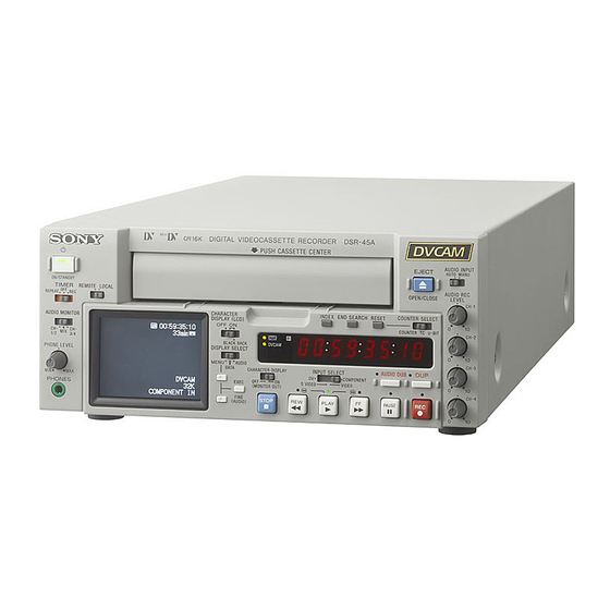
DIGITAL VIDEO CASSETTE RECORDER
RMT-DS5
US Model
Canadian Model
AEP Model
UK Model
E Model
Australian Model
New Zealand Model
R MECHANISM
TC IN
BNC type
0.5 to 18 Vp-p (time code input)
0.5 to 4 Vp-p (through output)
Outputs
MONITOR VIDEO
Phono jack, 1 Vp-p (75 ohms,
unbalanced) (superimpose)
VIDEO OUT
BNC type, 1 Vp-p (75 ohms,
unbalanced)
COMPONENT OUT
Y: BNC type
1.0 Vp-p (75 ohms, unbalanced)
R-Y: BNC type
0.7 Vp-p (75 ohms, unbalanced)
(DSR-45: 75%, color bars / DSR-
45P: 100%, colour bars)
B-Y: BNC type
0.7 Vp-p (75 ohms, unbalanced)
(DSR-45: 75%, color bars / DSR-
45P: 100%, colour bars)
S VIDEO OUT
Mini DIN 4-pin
Luminance signal: 1.0 Vp-p
(75 ohms, unbalanced)
Chrominance signal:
0.286 Vp-p (DSR-45)
0.3 Vp-p (DSR-45P)
(75 ohms, unbalanced)
AUDIO OUT (CH-1 to CH-4)
XLR 3-pin, male, +4 dBu, 600
ohms loading, balanced
MONITOR AUDIO
Phono jack
TC OUT
BNC type, 2.2 Vp-p, 600 ohms /
1.2 Vp-p, 75 ohms
0.5 to 4 Vp-p (through output,
600 ohms)
PHONES
Stereo minijack, 8 Ω
– Continued on next page –
DSR-45
DSR-45P
Advertisement
Table of Contents

Related Manuals for Sony DSR-45


Summary of Contents for Sony DSR-45
- Page 1 R-Y: BNC type 0.286 Vp-p (DSR-45) Quantization 8-bit 0.7 Vp-p (75 ohms, unbalanced) 0.3 Vp-p (DSR-45P) Sampling frequency (DSR-45: 75%, color bars / DSR- (75 ohms unbalanced) DSR-45: 45P: 100%, colour bars) COMPONENT IN 13.5 MHz (4:1:1 Component) B-Y: BNC type...
- Page 2 SONY PARTS WHOSE PART NUMBERS APPEAR AS DE FONCTIONNEMENT. NE REMPLACER CES COM- SHOWN IN THIS MANUAL OR IN SUPPLEMENTS PUB- POSANTS QUE PAR DES PIÈCES SONY DONT LES NUMÉROS SONT DONNÉS DANS CE MANUEL OU LISHED BY SONY. DANS LES SUPPLÉMENTS PUBLIÉS PAR SONY.
- Page 3 DSR-45/45P SAFETY CHECK-OUT (US Model only) After correcting the original service problem, perform the following safety checks before releasing the set to the customer: 1. Check the area of your repair for unsoldered or poorly-sol- UNLEADED SOLDER dered connections. Check the entire board surface for solder Boards requiring use of unleaded solder are printed with the lead- splashes and bridges.
-
Page 4: Table Of Contents
DSR-45/45P TABLE OF CONTENTS Section Title Page Section Title Page SERVICE NOTE PRINTED WIRING BOARDS AND ..............7 SCHEMATIC DIAGRAMS ........4-1 Note for Repair ............7 4-1. Frame Schematic Diagram (1/2) ......... 4-3 Frame Schematic Diagram (2/2) ......... 4-5 SELF-DIAGNOSIS FUNCTION 4-2. - Page 5 DSR-45/45P Section Title Page Section Title Page • VD-032 ..............4-127 3-22. Components of Drum Assembly • CM-59 ..............4-131 (Motor FPC Assembly, Elastic Connector) .... 5-22 • MD-76 ..............4-135 3-23. Components of Pinch Arm Assembly (Tape Retainer, •...
- Page 6 Internal Time Code Output Waveform Check ..5-98 Playback Blanking Level Adjustment with 7.5% Internal Time Code Output Check ......5-98 Setup (VD-032 Board)(DSR-45) ......5-63 3-8. Arrangement Diagram for Adjustment Parts ..5-99 Playback Y Signal Level Adjustment with 7.5% Setup (VD-032 Board)(DSR-45) ......
-
Page 7: Service Note
DSR-45/45P SERVICE NOTE NOTE FOR REPAIR When remove a connector, don’t pull at wire of connector. It is possible that a wire is snapped. Make sure that the flat cable and flexible board are not cracked of bent at the terminal. -
Page 8: Self-Diagnosis Function
DSR-45/45P SELF-DIAGNOSIS FUNCTION Self-diagnosis Function Self-diagnosis Display When problems occur while the unit is operating, the time code of When problems occur while the unit is operating, the self-diagno- the LCD monitor shows a 4-digit display consisting of an alpha- sis function starts working, and displays on the LCD monitor what bet and numbers, which blinks at 3.2 Hz. -
Page 9: Self-Diagnosis Code Table
DSR-45/45P Self-diagnosis Code Table Self-diagnosis Code Block Detailed Symptom/State Correction Function Code Condensation. Remove the cassette, and insert it again after one hour. Video head is dirty. Clean with the optional cleaning cassette. LOAD direction. Loading does not Load the tape again, and perform operations from the beginning. -
Page 10: General
14 times normal speed (DSR- • i.LINK (DV) : i.LINK-compliant DV jack (4-pin) The main features of the DSR-45/45P are described 45) or up to 17 times normal speed (DSR-45P) in both allows input or output of digital video/audio signals below. - Page 11 5 AUDIO MONITOR selector qa EJECT (OPEN/CLOSE) (open/close the cassette MANU) the unit, the unit accepts signals from any Sony compartment) button Use to select the audio track you want to listen to Remote Commander whose command mode is set to –...
- Page 12 The indicator lights while the unit is in the For details, see “EE/PB SEL” in the “DISPLAY SET menu” 2 AUDIO REC LEVEL control knobs on page 85 (GB). For details on time codes, see “DSR-45/ pause mode. CH-3 45P time codes”...
- Page 13 • If video signals have been input to the DV jack and from the MONITOR VIDEO jack, sync and burst are and the C (chroma: 3.58 MHz for DSR-45 and 4.43 are not superimposed. you output these video signals to the MONITOR not synchronized.
-
Page 14: Displaying Various Data
WIRELESS to enable the Remote Commander to control the unit. VTR RMT-DS5 • In addition to the Remote Commander supplied with the unit, the unit accepts signals from any Sony 6 PLAY button 7 FF button Remote Commander whose command mode is set to Notes on batteries VTR4. -
Page 15: Notes On Video Cassettes
Tape window facing upward system (i.e., PAL for the DSR-45, or NTSC for the During recording, if you change the INPUT SELECT DSR-45P), the image, sound and time code may be... -
Page 16: Playback
– Set EE/PB SEL on the DISPLAY SET menu to PB. If you record on a tape using a Sony digital camcorder of your computer or the user’s manuals of the software –... - Page 17 Notes if the signals for a certain search type are not recorded, PHOTO SEARCH. • When the command mode of a Sony device / remote you cannot perform that type of search. For details on commander is set to VTR4;...
-
Page 18: Recording
• When connecting a device that has a 6-pin DV jack to Monitor this unit, first, connect the plug of the cable to the 6- DSR-45/45P (rear panel) S-video output pin DV jack. • If the unit is connected to a device equipped with a 6-... -
Page 19: Notes On Usage In The Editing System
Connect this unit to an external AC timer (not supplied). To release the AC timer recording mode Player in an Editing Set the TIMER selector on the front panel of this unit to OFF. DSR-45/45P (rear panel) System Recording source (external tuner, etc.) VIDEO IN REF. -
Page 20: Connections For A Cut Editing System
The preroll time of the setting on the editing controller For details of connecting devices other than the DSR-45/ is required to be more than five seconds. For details on the settings of the Editing Control Unit, 45P, refer to the instruction manual of each device. -
Page 21: Adjusting Edit Timing
( ). 450/450CE DSR-45/45P’s operation mode, alarm messages, and • When using an FXE-100/100P that has been other information displayed as text on the monitor upgraded with an FXE-KIT1, the relevant menu item Set the SYNCHRO selector to ON. -
Page 22: Setting The Time Code And User Bits
• To set the user bits, you need to set TC/UB IN on the TC ⁄ UB SET TC ⁄ UB SET For details, see “DSR-45/45P time codes” on page 63 TC PRESET 00:00:00:00 TC/UB SET menu to INTERNAL beforehand. -
Page 23: Synchronizing The Time Codes
DF: Selects the drop frame mode. other analog connections. portion of the tape, the time code starts from NDF: Selects the non-drop frame mode. For details, see “DSR-45/45P time codes” on page 63 00:00:00:00. (GB). Note PRESET: The time code starts from the value set in •... -
Page 24: Adjusting The Sync And Subcarrier Phases Of The Video Signals
DSR-45/45P Adjusting the Sync and Subcarrier Phases of the Video Signals • If the external time code input is discontinuous or When you adjust the phases of the video signals, follow the steps below. does not advance correctly, the time code input may... -
Page 25: Duplication (Generating A Work Tape With The Same Time Code)
PLAY button on this unit. tape will be completely erased. • When both the recorder and the player are DSR-45/ This unit and the player will automatically rewind 45Ps, set the REMOTE/LOCAL switch of the player the tape to the beginning. -
Page 26: Audio Dubbing
If any warning message not listed in the table is cassette does not have cassette memory and duplication Monitor displayed, consult your Sony dealer. of the cassette memory will be cancelled. The duplicate operation will be completed without duplicating the cassette memory and this warning message will not be displayed. - Page 27 Playback still delay can be set between 0 and 10 frames by 11 steps. You can set the delay • This menu is displayed only for the DSR-45. which the unit turns to playback mode from still mode. (only for an RS-422A connection) •...
- Page 28 DSR-45/45P Operating the Menus Submenu Submenu Icon/Menu Setting Icon/Menu Setting (page) (page) REMOTE 232C RATE Selects the baud rate via the RS-232C connector. CM SET TAPE LABEL Makes a tape label. (You can enter up to 10 characters on a tape label.) 9600 : 9600 bps If you select this item, one of the following symbols appears.
- Page 29 Note OFF : Does not display the data codes. DATE: Displays the date when recorded. The default is M/D/Y for the DSR-45; and D/M/Y for the DSR-45P. CAMERA: Displays the camera data. TIME DISP Selects the form of the time displayed on the search screen or of the data codes and so on.
- Page 30 • The standard output level of the AUDIO OUT connectors is +4 dBu. This is equivalent to Notes –20 dB for the DSR-45, or –18 dB for the DSR-45P from full bit (maximum audio level). • The unit can record only in the DVCAM format or in the SP mode of the DV format.
-
Page 31: Troubleshooting
Set the TIMER selector to OFF. • If you use a PAL formatted tape in the DSR-45 (or use an NTSC formatted tape The TIMER selector is set to REPEAT. t When the TIMER selector is set to... -
Page 32: Alarm Messages
DVCAM not affect the recorded picture in any way. menu. Use them as guidelines for scheduling reconnecting it, cleaning cassette or a Sony Digital Video Cleaning Do not place this unit with the LCD screen pointing maintenance. operate the unit. -
Page 33: Disassembly
DSR-45/45P SECTION 2 DISASSEMBLY Note: Follow the disassembly procedure in the numerical order given. 2-1. UPPER CASE, BOTTOM PLATE 3 Upper case 2 Two screws (M3 case) 1 Two screws (M3 case) 5 Bottom plate 4 Six screws (B3) 2-2. FRONT PANEL BLOCK ASSEMBLY... -
Page 34: Fr-183/Dl-062 Boards
DSR-45/45P 2-3. FR-183/DL-062 BOARDS 4 Two screws (2 × 6) 5 Sheet metal (L), ground 6 Bracket (L) assembly 7 Door block 2 Two screws (2 × 6) 0 FR-183 board qa Harness (VD-060) (CN601) Switches 3 Sheet metal (R), ground... -
Page 35: Mechanism Deck
DSR-45/45P 2-5. MECHANISM DECK 3 Two screws (B3) 7 Flat cable (FVJ-020) 4 Flame T (CN1101) 6 Two step screws 8 Flat cable (FVJ-021) (CN6001) 9 Flat cable (FVJ-019) 5 Two screws (B3) (CN7002) qf Four screws (2 × 4.5) q;... -
Page 36: Jc-21/Di-73 Boards
DSR-45/45P 2-7. JC-21/DI-73 BOARDS 2 JC shield case 6 JC-21 board 1 Four screws (T2 × 4.5) 7 Screw (B2 × 4) 3 Flat cable (FJC-1) qs DI-73 board (CN5005) qa DI shield case 4 Two flat cables (FRJ-1) (CN4401, 4402) 8 Screw (B2 ×... -
Page 37: Rear Panel Block Assembly
DSR-45/45P 2-9. REAR PANEL BLOCK ASSEMBLY 2 Harness 7 Three flat cables 1 Two screws (B3) (AC-249) (CN101) (FVL-001: CN701, FVR-013: CN502, 3 Harness FVR-014: CN501) qf Two screws (PD-116) (CN201) (B3) 5 Harness (CN1983) qg Rear panel block 6 Harness... -
Page 38: Circuit Boards Location-1 (Over All)
DSR-45/45P 2-10. CIRCUIT BOARDS LOCATION-1 (OVER ALL) RS-083 RS-082 LS-060 JK-216 DV-032 CK-107 HP-135 XL-005 Power block Inverter trans unit VD-032 FM-037 PD-170 DL-062 FC-087 FR-183 Board Name Function DV-032 DV CONNECTOR VD-032 SYNC GENERATOR, VIDEO IN, UVIC, VIDEO OUT, AUDIO,... -
Page 39: Circuit Boards Location-2 (Mechanism Deck)
DSR-45/45P 2-11. CIRCUIT BOARDS LOCATION-2 (MECHANISM DECK) RP-234 JC-21 MD-76 DI-73 CM-59 Board Name Function MD-76 TAPE SENSOR RP-234 REC/PB AMP JC-21 VIDEO PB AMP, VIDEO A/D CONVERTER, CHROMA MIX, AFC, VFD, SFD, TFD, DV INTERFACE, MECHANISM CONTROL, AUDIO, POWER SUPPLY... -
Page 40: Block Diagrams
DSR-45/45P SECTION 3 BLOCK DIAGRAMS 3-1. OVERALL BLOCK DIAGRAM 1 ( ): Number in parenthesis ( ) indicates the division number of schematic diagram where the component is located. VD-032 BOARD (1/5) CN104 (1/2) CN202 (1/2) B-Y IN J105 (1/2) -
Page 41: Overall Block Diagram 2
DSR-45/45P 3-2. OVERALL BLOCK DIAGRAM 2 ( ): Number in parenthesis ( ) indicates the division number of schematic diagram where the component is located. JC-21 BOARD (1/6) DV-032 CN8001 (1/7) JIG PIN BOARD (FOR CHECK) 13 15 17 MY00 – 07 19 21 23 ı... -
Page 42: Overall Block Diagram 3
DSR-45/45P 3-3. OVERALL BLOCK DIAGRAM 3 ( ): Number in parenthesis ( ) indicates the division number of schematic diagram where the component is located. JC-21 BOARD (2/6) DI-73 BOARD (1/3) CN9500 (1/5) IC9013 CN9500 CN8001 CN1101 IC9016 IC9004 (2/5) -
Page 43: Overall Block Diagram 4
DSR-45/45P 3-4. OVERALL BLOCK DIAGRAM 4 ( ): Number in parenthesis ( ) indicates the division number of schematic diagram where the component is located. VD-032 BOARD(2/5) CN1501 (2/4) MONITOR Y OUT IC2015 IC2013 OVERALL2 MONITOR C OUT MONITOR (3-4) -
Page 44: Overall Block Diagram 5
DSR-45/45P 3-5. OVERALL BLOCK DIAGRAM 5 ( ): Number in parenthesis ( ) indicates the division number of schematic diagram where the component is located. M903 CN400 JC-21 BOARD (3/6) CM-59 BOARD CN5005 (1/2) CN001 (1/2) CAP FG CAP FG... -
Page 45: Overall Block Diagram 6
DSR-45/45P 3-6. OVERALL BLOCK DIAGRAM 6 ( ): Number in parenthesis ( ) indicates the division number of schematic diagram where the component is located. PD-170 BOARD VD-032 BOARD (3/5) CN1502 CN802 CN1504 PANEL COM PANEL COM LCD CHECK IC801 ı... -
Page 46: Overall Block Diagram 7
DSR-45/45P 3-7. OVERALL BLOCK DIAGRAM 7 ( ): Number in parenthesis ( ) indicates the division number of schematic diagram where the component is located. XL-005 BOARD VD-032 BOARD (4/5) JC-21 BOARD (4/6) CN1629 CN251 CH1+ CN8001 (5/7) CN1625 CN7001... -
Page 47: Overall Block Diagram 8
DSR-45/45P 3-8. OVERALL BLOCK DIAGRAM 8 ( ): Number in parenthesis ( ) indicates the division number of schematic diagram where the component is located. DI-73 BOARD (2/3) IC7005 CN9500 (3/5) (DI-73 (5/9)) CN9500 (4/5) AU X1 IN AU CH1 OUT... -
Page 48: Overall Block Diagram 9
DSR-45/45P 3-9. OVERALL BLOCK DIAGRAM 9 ( ): Number in parenthesis ( ) indicates the division number of schematic diagram where the component is located. RS-083 BOARD FR-183 BOARD FC-087 BOARD FM-037 BOARD VD-032 BOARD (5/5) S352 OVERALL1 XRESET S811... -
Page 49: Power Block Diagram 1
DSR-45/45P 3-10. POWER BLOCK DIAGRAM 1 ( ): Number in parenthesis ( ) indicates the division number of schematic diagram where the component is located. POWER BLOCK (ACS1581-MA) VD-032 BOARD (1/2) AC IN F1985 +12V UNSW POWER2 CN101 D101 CN201... -
Page 50: Power Block Diagram 2
DSR-45/45P 3-11. POWER BLOCK DIAGRAM 2 ( ): Number in parenthesis ( ) indicates the division number of schematic diagram where the component is located. VD-032 BOARD (2/2) IC2014 IC2001 IC2005 IC2006 IC2003 IC2004 IC2009 IC2007 IC2010 IC2019 IC2020 IC2021... -
Page 51: Power Block Diagram 3
DSR-45/45P 3-12. POWER BLOCK DIAGRAM 3 ( ): Number in parenthesis ( ) indicates the division number of schematic diagram where the component is located. JC-21 BOARD IC1105 IC1101 IC1103 IC1000 IC1102 IC1104 IC1106 IC1108 IC1109 IC1110 REF DC IC1001 REF DC GEN. -
Page 52: Power Block Diagram 4
DSR-45/45P 3-13. POWER BLOCK DIAGRAM 4 ( ): Number in parenthesis ( ) indicates the division number of schematic diagram where the component is located. DI-73 BOARD IC9500 IC9509 IC9001 IC9503 IC9512 IC9007 IC9506 IC9010 SYNC IC9000 SHIFTER IC9017 (DI-73 (3/9, 4/9)) -
Page 53: Power Block Diagram 5
DSR-45/45P 3-14. POWER BLOCK DIAGRAM 5 ( ): Number in parenthesis ( ) indicates the division number of schematic diagram where the component is located. CM-59 BOARD IC102 IC300 IC400 IC500 CN500 M901 BUFFER LOADING CAPSTAN DRUM/C SENSOR VCC DRUM... -
Page 54: Printed Wiring Boards And Schematic Diagrams
DSR-45/45P SECTION 4 PRINTED WIRING BOARDS AND SCHEMATIC DIAGRAMS THIS NOTE IS COMMON FOR PRINTED WIRING BOARDS AND SCHEMATIC DIAGRAMS. (In addition to this, the necessary note is printed in each block) For printed wiring boards: Measuring conditions voltege and waveform: •... - Page 55 DSR-45/45P 4-1. FRAME SCHEMATIC DIAGRAM (1/2) CONTINUED ON JD-054 HARNESS PAGE 4-5 CONTINUED ON CN301 CN1628 FVJ-021 FLAT CABLE CN904 PAGE 4-5 HP+4V HP+4V SW_+6V EVR_+3V HP-135 CONTINUED ON HP-4V HP-4V VIDEO +5V FVJ-020 FLAT CABLE PAGE 4-5 MUTE MUTE...
-
Page 56: Frame Schematic Diagram (1/2)
DSR-45/45P FRAME SCHEMATIC DIAGRAM (2/2) CD-116 HARNESS CONTINUED ON PAGE 4-4 M905 M902 M901(1/2) CONTINUED ON VJ-108 HARNESS FL MOTOR CAM MOTOR DRUM HEAD PAGE 4-4 M901 JD-054 HARNESS M904 M903 CONTINUED ON (2/2) REEL CAPSTAN PAGE 4-4 DRUM MOTOR... -
Page 57: Schematic Diagrams
DSR-45/45P 4-2. SCHEMATIC DIAGRAMS RP-234 (1/2) (REC/PB AMP 1) • See page 4-115 for RP-234 printed wiring board. • See page 4-161 for waveforms. RP-234 BOARD (1/2) REC/PB AMP 1 XX MARK:NO MOUNT RF6V NO MARK:REC/PB MODE R:REC MODE P:PB MODE... -
Page 58: 2/2)(Rec/Pb Amp 2)
DSR-45/45P RP-234 (2/2) (REC/PB AMP 2) • See page 4-115 for RP-234 printed wiring board. • See page 4-161 for waveforms. RP-234 BOARD (2/2) REC/PB AMP 2 XX MARK:NO MOUNT NO MARK:REC/PB MODE R:REC MODE P:PB MODE RF6V RP-234 BOARD (1/2) - Page 59 DSR-45/45P JC-21 (1/14) (VIDEO PB AMP) • See page 4-119 for JC-21 printed wiring board. • See page 4-162 for waveforms. JC-21 BOARD (1/14) VIDEO PB AMP XX MARK:NO MOUNT NO MARK:REC/PB MODE JC-21 BOARD (4/14) AFC_Y Y_IN JC-21 BOARD (14/14)
- Page 60 DSR-45/45P JC-21 (2/14) (VIDEO A/D CONVERTER) • See page 4-119 for JC-21 printed wiring board. • See page 4-162, 163 for waveforms. JC-21 BOARD (2/14) VIDEO A/D CONVERTER SPCK1 JC-21 BOARD (4/14) JC-21 BOARD (14/14) VIDEO_-5V C1180 R1211 L1114 10uH...
- Page 61 DSR-45/45P JC-21 (3/14) (CHROMA MIX) • See page 4-119 for JC-21 printed wiring board. JC-21 BOARD (3/14) CHROMA MIX XX MARK:NO MOUNT NO MARK:REC/PB MODE R:REC MODE P:PB MODE IC2214 IC2215 IC2214 IC2209 TC74VHC374FT(EL) TC74VHC244FT(EL) R2250 IC2215 TC74VHC541FT(EL) IC2212 R1.4/P3.2 R1.3/P2.8...
- Page 62 DSR-45/45P JC-21 (4/14) (AFC) • See page 4-119 for JC-21 printed wiring board. • See page 4-163, 164 for waveforms. JC-21 BOARD (4/14) XX MARK:NO MOUNT NO MARK:REC/PB MODE R:REC MODE P:PB MODE 17-2 R2253 17-1 R2256 CL2236 JC-21 BOARD (3/14)
-
Page 63: Vfd(Video Dsp,D/A Converter)
DSR-45/45P JC-21 (5/14) (VFD (VIDEO DSP, D/A CONVERTER)) • See page 4-119 for JC-21 printed wiring board. • See page 4-164, 165 for waveforms. JC-21 BOARD (5/14) VFD(VIDEO DSP,D/A CONVERTER) XX MARK:NO MOUNT NO MARK:REC/PB MODE R:REC MODE P:PB MODE... - Page 64 DSR-45/45P JC-21 (6/14) (SFD) • See page 4-119 for JC-21 printed wiring board. • See page 4-165 for waveforms. JC-21 BOARD (6/14) XX MARK:NO MOUNT NO MARK:REC/PB MODE R:REC MODE P:PB MODE :IMPOSSIBLE TO MEASURE THE VOLTAGE AT THE MARKED POINTS.
- Page 65 DSR-45/45P JC-21 (7/14) (TFD) • See page 4-119 for JC-21 printed wiring board. JC-21 BOARD (7/14) XX MARK:NO MOUNT NO MARK:REC/PB MODE R:REC MODE P:PB MODE RF_6V JC-21 BOARD (9/14) JC-21 BOARD (8/14) 41-1 CN4401 RF 6V RF 6V C1ERRP C4420 0.01u...
- Page 66 DSR-45/45P JC-21 (8/14) (DV INTERFACE) • See page 4-119 for JC-21 printed wiring board. JC-21 BOARD (8/14) DV INTERFACE XX MARK:NO MOUNT R4430 R4425 NO MARK:REC/PB MODE R:REC MODE P:PB MODE 39-1 39-2 XDVCN LBUS3 LBUS2 XRST_PHY LIP_SLEEP LBUS1 R2.8/P2.1...
-
Page 67: 9/14) (Mechanism Control 1)
DSR-45/45P JC-21 (9/14) (MECHANISM CONTROL 1) • See page 4-119 for JC-21 printed wiring board. JC-21 BOARD (9/14) MECHANISM CONTROL 1 NO MARK:REC/PB MODE R:REC MODE XX MARK:NO MOUNT P:PB MODE RF_6V L5001 10uH JC-21 BOARD (7/14) J_3V J_3V JC-21 BOARD (10/14) -
Page 68: 10/14) (Mechanism Control 2)
DSR-45/45P JC-21 (10/14) (MECHANISM CONTROL 2) • See page 4-119 for JC-21 printed wiring board. • See page 4-165 for waveforms. JC-21 BOARD (10/14) MECHANISM CONTROL 2 XX MARK:NO MOUNT NO MARK:REC/PB MODE R:REC MODE P:PB MODE J_3V IC5008 JC-21 BOARD (9/14) -
Page 69: 11/14) (Mode Control)
DSR-45/45P JC-21 (11/14) (MODE CONTROL) • See page 4-119 for JC-21 printed wiring board. • See page 4-166 for waveforms. JC-21 BOARD (11/14) MODE CONTROL XX MARK:NO MOUNT NO MARK:REC/PB MODE R:REC MODE Q6003 P:PB MODE UN9113J-(K8).SO R6059 MO73 R6057... -
Page 70: 12/14) (Audio 1)
DSR-45/45P JC-21 (12/14) (AUDIO 1) • See page 4-119 for JC-21 printed wiring board. JC-21 BOARD (12/14) AUDIO 1 XX MARK:NO MOUNT J_3V JC-21 BOARD (14/14) R7009 CN7001 CL7032 CH1 OUT CL7033 R7011 GND(CH1 OUT) C7015 CL7034 R7010 XX VD-032 BOARD (11/16) CH2 OUT 6.3V... -
Page 71: 13/14) (Audio 2)
DSR-45/45P JC-21 (13/14) (AUDIO 2) • See page 4-119 for JC-21 printed wiring board. JC-21 BOARD (13/14) AUDIO 2 XX MARK:NO MOUNT CN7002 CL7004 AU X1 IN AU_X1_IN CL7005 AU_Y1_IN AU Y1 IN(GND) CL7006 AU_1_GND_IN CL7007 AU_X2_IN AU X2 IN... -
Page 72: 14/14) (Power Supply)
DSR-45/45P JC-21 (14/14) (POWER SUPPLY) • See page 4-119 for JC-21 printed wiring board. SIGNAL PATH JC-21 BOARD (14/14) VIDEO SIGNAL AUDIO SIGNAL POWER SUPPLY CHROMA XX MARK:NO MOUNT NO MARK:REC/PB MODE J_3V JC-21 BOARD (11/14) J_3V JC-21 BOARD (12/14) - Page 73 DSR-45/45P DI-73 (1/9) (VIDEO D/A CONVERTER) • See page 4-123 for DI-73 printed wiring board. • See page 4-167 for waveforms. DI-73 BOARD (1/9) VIDEO D/A CONVERTER XX MARK:NO MOUNT NO MARK:REC/PB MODE Q9001 DPB_YOUT 2SC4081T106R VIDEO_5V L9002 DPB_CROUT VIDEO_-5V...
-
Page 74: 2/9) (Video Fifo Memory)
DSR-45/45P DI-73 (2/9) (VIDEO FIFO MEMORY) • See page 4-123 for DI-73 printed wiring board. DI-73 BOARD (2/9) VIDEO FIFO MEMORY XX MARK:NO MOUNT NO MARK:REC/PB MODE R:REC MODE P:PB MODE J-3V SPCK2 IC9011 R9034 IC9011 M66280FP-280D JC00 JC01 JC02... -
Page 75: 3/9) (Sync Shifter 1)
DSR-45/45P DI-73 (3/9) (SYNC SHIFTER 1) • See page 4-123 for DI-73 printed wiring board. DI-73 BOARD (3/9) SYNC SHIFTER 1 XX MARK:NO MOUNT NO MARK:REC/PB MODE VIDEO_5V R:REC MODE 10-1 P:PB MODE IC9506 IC9503 J_3V IC9506 TC74VHC163FT(EL) VIDEO_5V IC9503... -
Page 76: 4/9) (Sync Shifter 2)
DSR-45/45P DI-73 (4/9) (SYNC SHIFTER 2) • See page 4-123 for DI-73 printed wiring board. DI-73 BOARD (4/9) SYNC SHIFTER 2 XX MARK:NO MOUNT NO MARK:REC/PB MODE IC9509 IC9512 IC9509 TC74VHC163FT(EL) IC9512 TC74VHC163FT(EL) VIDEO_5V 10-1 C9506 0.1u C9508 10-2 0.1u... - Page 77 DSR-45/45P DI-73 (5/9) (AUDIO HPF) • See page 4-123 for DI-73 printed wiring board. DI-73 BOARD (5/9) AUDIO HPF XX MARK:NO MOUNT A.-5V NO MARK:REC/PB MODE A.+5V 13-1 AU_X2_IN R7095 R7086 AU_Y2_IN 4700 4700 13-2 AU_2_GND_IN R7030 R7008 C7000 R7024 R7014 0.22u...
-
Page 78: 6/9) (Audio A/D, D/A Converter)
DSR-45/45P DI-73 (6/9) (AUDIO A/D, D/A CONVERTER) • See page 4-123 for DI-73 printed wiring board. DI-73 BOARD (6/9) AUDIO A/D,D/A CONVERTER XX MARK:NO MOUNT NO MARK:REC/PB MODE :IMPOSSIBLE TO MEASURE THE VOLTAGE AT THE MARKED POINTS. A.-5V A.+5V A.+5V 13-1 +2.8V... -
Page 79: 8/9) (Audio Dsp Control)
DSR-45/45P DI-73 (7/9) (AUDIO DSP) • See page 4-123 for DI-73 printed wiring board. • See page 4-167 for waveforms. DI-73 BOARD (7/9) AUDIO DSP XX MARK:NO MOUNT NO MARK:REC/PB MODE :IMPOSSIBLE TO MEASURE THE VOLTAGE AT THE MARKED POINTS. - Page 80 DSR-45/45P DI-73 (8/9) (AUDIO DSP CONTROL) • See page 4-123 for DI-73 printed wiring board. • See page 4-167 for waveform. DI-73 BOARD (8/9) TC/REC_DATA AUDIO DSP CONTROL TC/PB_DATA DI-73 BOARD (9/9) XX MARK:NO MOUNT TC/XTHRU NO MARK:REC/PB MODE TC_XNT :IMPOSSIBLE TO MEASURE THE VOLTAGE AT THE MARKED POINTS.
-
Page 81: 9/9) (Time Code In/Out)
DSR-45/45P DI-73 (9/9) (TIME CODE IN/OUT) • See page 4-123 for DI-73 printed wiring board. DI-73 BOARD (9/9) Q8202 2SC4081T106R LND9501 TIME CODE IN/OUT R8014 IC8004 XX MARK:NO MOUNT LND9502 NO MARK:REC/PB MODE C8012 IC8006 R8015 R8010 R8026 6800 TC/IN... - Page 82 DSR-45/45P VD-032 (1/16) (SYNC GENERATOR 1) • See page 4-127 for VD-032 printed wiring board. • See page 4-168 for waveforms. VD-032 BOARD (1/16) SYNC GENERATOR 1 XX MARK:NO MOUNT NO MARK:REC/PB MODE R:REC MODE P:PB MODE C012 R008 R011 0.1u...
- Page 83 DSR-45/45P VD-032 (2/16) (SYNC GENERATOR 2) • See page 4-127 for VD-032 printed wiring board. • See page 4-168, 169 for waveforms. VD-032 BOARD (2/16) VIDEO_+9V VD-032 BOARD (14/16) SYNC GENERATOR 2 XX MARK:NO MOUNT R141 R144 4700 4700 NO MARK:REC/PB MODE...
- Page 84 DSR-45/45P VD-032 (3/16) (SYNC GENERATOR 3) • See page 4-127 for VD-032 printed wiring board. • See page 4-169 for waveforms. VD-032 BOARD (3/16) SYNC GENERATOR 3 XX MARK:NO MOUNT NO MARK:REC/PB MODE R:REC MODE P:PB MODE :IMPOSSIBLE TO MEASURE THE VOLTAGE AT THE MARKED POINTS.
- Page 85 DSR-45/45P VD-032 (4/16) (VIDEO IN 1) • See page 4-127 for VD-032 printed wiring board. • See page 4-169, 170 for waveforms. R381 R394 VD-032 BOARD (4/16) VIDEO_+5V VD-032 BOARD (15/16) 38-2 R383 R395 C353 VIDEO IN 1 Q241 Q244...
- Page 86 DSR-45/45P VD-032 (5/16) (VIDEO IN 2) • See page 4-127 for VD-032 printed wiring board. • See page 4-171 for waveforms. VD-032 BOARD (5/16) 48-1 C232 R211 R228 R238 2200 6.3V VIDEO IN 2 R250 R212 Q204 C231 R214 C233...
- Page 87 DSR-45/45P VD-032 (6/16) (VIDEO IN 3) • See page 4-127 for VD-032 printed wiring board. • See page 4-171, 172 for waveforms. VD-032 BOARD (6/16) DIG/XANA VD-032 BOARD (3/16) VIDEO IN 3 GEN_REF_Y VD-032 BOARD (2/16) XX MARK:NO MOUNT VIDEO_+5V...
- Page 88 DSR-45/45P VD-032 (7/16) (UVIC) • See page 4-127 for VD-032 printed wiring board. • See page 4-172 for waveforms. VD-032 BOARD (7/16) UVIC XX MARK:NO MOUNT NO MARK:REC/PB MODE R:REC MODE P:PB MODE Q1501 L1501 Q1502 2SC4081T106R 10uH 2SC4081T106R VIDEO_+5V...
- Page 89 DSR-45/45P VD-032 (8/16) (VIDEO OUT 1) • See page 4-127 for VD-032 printed wiring board. • See page 4-172, 173 for waveforms. SIGNAL PATH VD-032 BOARD (8/16) VIDEO SIGNAL VIDEO OUT 1 CHROMA Y/CHROMA XX MARK:NO MOUNT NO MARK:REC/PB MODE...
- Page 90 DSR-45/45P VD-032 (9/16) (VIDEO OUT 2) • See page 4-127 for VD-032 printed wiring board. • See page 4-173, 174 for waveforms. VD-032 BOARD (9/16) VIDEO OUT 2 XX MARK:NO MOUNT NO MARK:REC/PB MODE VD-032 BOARD (2/16) R_Y_BLK 98-1 L2006...
-
Page 91: 10/16) (Video Out 3)
DSR-45/45P VD-032 (10/16) (VIDEO OUT 3) • See page 4-127 for VD-032 printed wiring board. • See page 4-174, 175 for waveforms. VD-032 BOARD (10/16) VIDEO OUT 3 XX MARK:NO MOUNT NO MARK:REC/PB MODE L2001 10uH R:REC MODE VIDEO_+5V P:PB MODE... -
Page 92: 11/16) (Audio)
DSR-45/45P VD-032 (11/16) (AUDIO) • See page 4-127 for VD-032 printed wiring board. VD-032 BOARD (11/16) AUDIO Q1628 Q1627 UN9113J-(K8).SO XX MARK:NO MOUNT UN9113J-(K8).SO AUDIO+5V NO MARK:REC/PB MODE R1627 R1628 AUDIO-5V VD-032 BOARD (15/16) 100k 100k C1638 C1634 C1640 R1765... -
Page 93: 12/16) (Hi Control)
DSR-45/45P VD-032 (12/16) (HI CONTROL) • See page 4-127 for VD-032 printed wiring board. • See page 4-175 for waveforms. NO MARK:REC/PB MODE HI60 VD-032 BOARD (12/16) XCS_RS :IMPOSSIBLE TO MEASURE THE VD-032 BOARD (13/16) XRS_RESET VOLTAGE AT THE MARKED POINTS. -
Page 94: 13/16) (Rs-232C/422 Control)
DSR-45/45P VD-032 (13/16) (RS-232C/422 CONTROL) • See page 4-127 for VD-032 printed wiring board. • See page 4-175 for waveforms. VD-032 BOARD (13/16) VD-032 BOARD (12/16) HI_UNSW_5V V_SYNC_RS VD-032 BOARD (12/16) RS-232C/422 CONTROL VD-032 BOARD (16/16) DIG_+5V XX MARK:NO MOUNT... -
Page 95: 14/16) (Dc In)
DSR-45/45P VD-032 (14/16) (DC IN) • See page 4-127 for VD-032 printed wiring board. VD-032 BOARD (14/16) Q623 D602 2SC4081T106R MA729-(K8).S0 16.6 13.2 LCD+13V DC IN R622 VD-032 BOARD (7/16) R624 XX MARK:NO MOUNT 13.8 LCD+6V NO MARK:REC/PB MODE Q621 16.6... -
Page 96: 15/16) (Dc/Dc Converter 1)
DSR-45/45P VD-032 (15/16) (DC/DC CONVERTER 1) • See page 4-127 for VD-032 printed wiring board. VD-032 BOARD (15/16) DC/DC CONVERTER 1 XX MARK:NO MOUNT NO MARK:REC/PB MODE :IMPOSSIBLE TO MEASURE THE VOLTAGE AT THE MARKED POINTS. LND901 S_GND LND900 S_GND... -
Page 97: 16/16) (Dc/Dc Converter 2)
DSR-45/45P VD-032 (16/16) (DC/DC CONVERTER 2) • See page 4-127 for VD-032 printed wiring board. VD-032 BOARD (16/16) NO MARK:REC/PB MODE :IMPOSSIBLE TO MEASURE THE VOLTAGE AT THE MARKED POINTS. DC/DC CONVERTER 2 XX MARK:NO MOUNT VD-032 BOARD (14/16) F1984... -
Page 98: 1/3) (Dc/Dc Converter, Reel Motor Drive)
DSR-45/45P CM-59 (1/3) (DC/DC CONVERTER, REEL MOTOR DRIVE) • See page 4-131 for CM-59 printed wiring board. CM-59 BOARD (1/3) DC/DC CONVERTER,REEL MOTOR DRIVE XX MARK:NO MOUNT NO MARK:REC/PB MODE Q105 UN9211J-(TX).SO IC101 R116 6.25V IC101 CM-59 BOARD (3/3) MM1385GNLE... -
Page 99: 2/3) (Drum Motor Drive, Fl Motor Drive)
DSR-45/45P CM-59 (2/3) (DRUM MOTOR DRIVE, FL MOTOR DRIVE) • See page 4-131 for CM-59 printed wiring board. • See page 4-176 for waveforms. CM-59 BOARD (2/3) DRUM MOTOR DRIVE,FL MOTOR DRIVE XX MARK:NO MOUNT NO MARK:REC/PB MODE CM-59 BOARD (1/3) -
Page 100: 3/3) (Capstan Motor Drive, Cam Motor Drive)
DSR-45/45P CM-59 (3/3) (CAPSTAN MOTOR DRIVE, CAM MOTOR DRIVE) • See page 4-131 for CM-59 printed wiring board. • See page 4-176 for waveforms. CM-59 BOARD (3/3) CAPSTAN MOTOR DRIVE,CAM MOTOR DRIVE XX MARK:NO MOUNT NO MARK:REC/PB MODE :IMPOSSIBLE TO MEASURE THE VOLTAGE AT THE MARKED POINTS. -
Page 101: Tape Sensor
VOLTAGE AT THE MARKED POINTS. CM-59 BOARD(1/3) CN200 THROUGH THE FMD-14 FLAT CABLE (SEE PAGE 4-90) M904 REEL MOTOR GAIN GAIN OFFSET OFFSET CM-59 BOARD(1/3) CN201 THROUGH THE FMD-14 FLAT CABLE (SEE PAGE 4-90) TLP907 (LB, SONY) TLP907 (LB, SONY) MD-76 4-95 4-96... -
Page 102: Ejection Detect Switch
DSR-45/45P CK-107 (EJECTION DETECT SWITCH)/DL-062 (REMOTE CONTROL RECEIVER) FC-087 (FRONT DOOR DETECT SWITCH)/FM-037 (FRONT DOOR MOTOR) • See page 4-137 for CK-107, DL-062 printed wiring board. • See page 4-138 for FC-087, FM-037 printed wiring board. CK-107 BOARD FC-087 BOARD... -
Page 103: User Control
DSR-45/45P FR-183 (USER CONTROL) • See page 4-139 for FR-183 printed wiring board. FR-183 BOARD USER CONTROL XX MARK:NO MOUNT IC403 ND407 ND406 ND403 ND408 ND405 ND404 ND402 ND401 R406 C413 NO MARK:REC/PB MODE LA-301VL1 LA-301VL1 LA-301VL1 LA-301VL1 LA-301VL1 LA-301VL1... -
Page 104: Head Phone
DSR-45/45P HP-135 (HEAD PHONE) • See page 4-143 for HP-135 printed wiring board. HP-135 BOARD HEAD PHONE NO MARK:REC/PB MODE IC301 IC301 NJM4556AM-A-TE2 PHONE R304 LEVEL R307 R303 RV301 R309 D301 D302 10k/10k FB301 MA3075WA-(TX) MA3075WA-(TX) FB302 -4.1 CN301 R308... -
Page 105: 1/2) (Rgb Driver)
DSR-45/45P PD-170 (1/2) (RGB DRIVER) • See page 4-145 for PD-170 printed wiring board. • See page 4-177 for waveforms. JL001 PD-170 BOARD (1/2) JL002 RGB DRIVER XX MARK:NO MOUNT JL003 INVERTER ND901 TRANSFORMER BACK NO MARK:REC/PB MODE UNIT LIGHT... -
Page 106: 2/2) (Timing Generator)
DSR-45/45P PD-170 (2/2) (TIMING GENERATOR) • See page 4-145 for PD-170 printed wiring board. • See page 4-177, 178 for waveforms. PD-170 BOARD (2/2) TIMING GENERATOR XX MARK:NO MOUNT IC902 NO MARK:REC/PB MODE L901 10uH PANEL_13.2V PANEL_-15.3V IC902 R929 L902... -
Page 107: Video/Audio In/Out
DSR-45/45P JK-216 (VIDEO/AUDIO IN/OUT) • See page 4-147 for JK-216 printed wiring board. JK-216 BOARD J106 COMPONENT VIDEO/AUDIO IN/OUT MONITOR XX MARK:NO MOUNT J103 J104 J105 VIDEO AUDIO D109 NO MARK:REC/PB MODE MAZ9120D0LS0-TX/L D102 D104 D105 D106 D107 D108 MAZ9120D0LS0-TX/L... -
Page 108: Audio Out
DSR-45/45P XL-005 (AUDIO OUT) • See page 4-151 for XL-005 printed wiring board. XL-005 BOARD AUDIO OUT XX MARK:NO MOUNT AUDIO OUT CH-1 CH-2 CH-3 CH-4 CN251 CN252 CN254 CN256 CN258 D252 CH1+ D251 MA3200WA-TX D253 D254 MA3200WA-TX MA3200WA-TX MA3200WA-TX... -
Page 109: Rs-422 Driver)/Rs-083 (Rs-232C Driver)
DSR-45/45P RS-082 (RS-422 DRIVER)/RS-083 (RS-232C DRIVER) DV-032 (DV CONNECTOR)/LS-060 (CONTROL JACK) • See page 4-153 for RS-082/RS-083 printed wiring board. • See page 4-155, 156 for DV-032/LS-060 printed wiring board. RS-082 BOARD NO MARK:REC/PB MODE SIGNAL PATH DV-032 BOARD RS-422 DRIVER... - Page 110 DSR-45/45P ACS1581-MA (POWER) • See page 4-157 for ACS1581-MA printed wiring board. POWER BLOCK(ACS1581-MA BOARD) Note:POWER BLOCK(ACS1581-MA BOARD)excluding F101(FUSE T2.5A/250V)is replaced as a block. POWER C203 C204 1000p 1000p R117 R202 100V 100V FB101 0.47 XX MARK:NO MOUNT 0.45uH 1/4W...
- Page 111 DSR-45/45P 4-3. PRINTED WIRING BOARDS RP-234 (REC/PB AMP) • For Printed Wiring Board. • RP-234 board is six-layer print board. However, the patterns of layers 2 to 5 have not been included in the diagram. • There are a few cases that the part isn't mounted in this model is printed on this diagram.
- Page 112 DSR-45/45P 4-117 4-118 RP-234...
- Page 113 DSR-45/45P JC-21 (VIDEO PB AMP, VIDEO A/D CONVERTER, CHROMA MIX, AFC, VFD, SFD, TFD, DV INTERFACE, MECHANISM CONTROL, AUDIO, POWER SUPPLY) • For Printed Wiring Board. • JC-21 board is six-layer print board. However, the patterns of layers 2 to 5 have not been included in the diagram.
- Page 114 DSR-45/45P 4-121 4-122 JC-21...
- Page 115 DSR-45/45P DI-73 (VIDEO D/A CONVERTER, SYNC SHIFTER, AUDIO A/D, D/A CONVERTER, AUDIO DSP, TIME CODE IN/OUT) • For Printed Wiring Board. • DI-73 board is four-layer print board. However, the patterns of layers 2 to 3 have not been included in the diagram.
- Page 116 DSR-45/45P 4-125 4-126 DI-73...
- Page 117 DSR-45/45P VD-032 (SYNC GENERATOR, VIDEO IN, UVIC, VIDEO OUT, AUDIO, HI CONTROL, RS232C/422 CONTROL, DC IN, DC/DC CONVERTER) • For Printed Wiring Board. • :Uses unleaded solder. • VD-032 board is six-layer print board. However, the patterns of layers 2 to 5 have not been included in the diagram.
- Page 118 DSR-45/45P CAUTION Danger of explosion if battery is incorrectly replaced. Replace only with the same or eqivalent type. 4-129 4-130 VD-032...
- Page 119 DSR-45/45P CM-59 (DC/DC CONVERTER, MOTOR DRIVE) • For Printed Wiring Board. • There are a few cases that the part isn't mounted in this model is printed on this diagram. • See page 4-180 for printed parts location. • Chip transistor...
- Page 120 DSR-45/45P 4-133 4-134 CM-59...
- Page 121 DSR-45/45P MD-76 (TAPE SENSOR) • For Printed Wiring Board. • MD-76 board is four-layer print board. However, the patterns of layers 2 to 3 have not been included in the diagram. • There are a few cases that the part isn't mounted in this model is printed on this diagram.
- Page 122 DSR-45/45P CK-107 (EJECTION DETECT SWITCH)/DL-062 (REMOTE CONTROL RECEIVER) FC-087 (FRONT DOOR DETECT SWITCH)/FM-037 (FRONT DOOR MOTOR) • For Printed Wiring Board. • :Uses unleaded solder. • There are a few cases that the part isn't mounted in this model is printed on this diagram.
- Page 123 DSR-45/45P FR-183 (USER CONTROL) • For Printed Wiring Board. • :Uses unleaded solder. • There are a few cases that the part isn't mounted in this model is printed on this diagram. • See page 4-181 for printed parts location.
- Page 124 DSR-45/45P AUDIO LEVEL INPUT SELECT COMPONENT VIDEO S VIDEO (RESET) 4-141 4-142 FR-183...
- Page 125 DSR-45/45P HP-135 (HEAD PHONE) • For Printed Wiring Board. • :Uses unleaded solder. • There are a few cases that the part isn't mounted in this model is printed on this diagram. • Chip transistor PHONES PHONE LEVEL HP-135 4-143...
- Page 126 DSR-45/45P PD-170 (RGB DRIVER, TIMING GENERATOR) • For Printed Wiring Board. • PD-170 board is five-layer print board. However, the patterns of layers 2 to 4 have not been included in the diagram. • There are a few cases that the part isn't mounted in this model is printed on this diagram.
- Page 127 DSR-45/45P JK-216 (VIDEO/AUDIO IN/OUT) JK-216 4-147 4-148...
- Page 128 DSR-45/45P • For Printed Wiring Board. • :Uses unleaded solder. • JK-216 board is three-layer print board. However, the patterns of layer 2 have not been included in the diagram. • There are a few cases that the part isn't mounted in this model is printed on this diagram.
- Page 129 DSR-45/45P XL-005 (AUDIO OUT) • For Printed Wiring Board. • :Uses unleaded solder. • XL-005 board is three-layer print board. However, the patterns of layer 2 have not been included in the diagram. • There are a few cases that the part isn't mounted in this model is printed on this diagram.
- Page 130 DSR-45/45P RS-082 (RS-422 DRIVER)/RS-083 (RS-232C DRIVER) • For Printed Wiring Board. • :Uses unleaded solder. • RS-082 and RS-083 boards are three-layer print board. However, the patterns of layer 2 have not been included in the diagram. • There are a few cases that the part isn't mounted in this model is printed on this diagram.
- Page 131 DSR-45/45P DV-032 (DV CONNECTOR) LS-060 (CONTROL JACK) • For Printed Wiring Board. • :Uses unleaded solder. • DV-032 and LS-060 boards are three-layer print board. However, the patterns of layer 2 have not been included in the diagram. • There are a few cases that the part isn't mounted in this model is printed on this diagram.
-
Page 132: Acs1581-Ma (Power)
DSR-45/45P ACS1581-MA (POWER) • For Printed Wiring Board. • There are a few cases that the part isn't mounted in this model is printed on this diagram. • See page 4-181 for printed parts location. ACS1581-MA BOARD C214 C208 C115... -
Page 133: Waveforms
DSR-45/45P 4-4. WAVEFORMS RP-234 BOARD 3.7 Vp-p 2.8 Vp-p 150 Hz 13.5 MHz IC301 ra REC/PB IC101 1, 2, 6, 7 REC 2.8 Vp-p 2.8 Vp-p 300 Hz 150 Hz IC301 tg REC/PB IC101 qa, qs REC 510 mVp-p 300 Hz IC101 wj PB 2.0 Vp-p... - Page 134 DSR-45/45P JC-21 BOARD (1/5) 260 mVp-p 1.7 Vp-p IC1000 1 REC/PB Q1117 B REC 1.0 Vp-p 250 mVp-p IC1002 1 REC/PB Q1118 B REC 240 mVp-p 1.1 Vp-p IC1112 1 REC/PB Q1119 B REC 240 mVp-p 1.7 Vp-p IC1001 1 REC/PB...
- Page 135 DSR-45/45P JC-21 BOARD (2/5) 3.3 Vp-p 1.1 Vp-p 0.16 µsec IC1108 1 8 REC Q2200 B PB − 1.0 Vp-p 1.6 Vp-p IC1109 wa REC Q2200 B REC 3.0 Vp-p 3.3 Vp-p 13.5 MHz 0.16 µsec IC1109 1 8 REC IC2204 rd REC/PB −...
- Page 136 DSR-45/45P JC-21 BOARD (3/5) 550 mVp-p 280 mVp-p IC2204 3, 7 PB IC3300 uh REC/PB 260 mVp-p 830 mVp-p IC2204 3, 7 REC IC3300 uf REC/PB 2.8 Vp-p 270 mVp-p 13.5 MHz IC2204 qd REC/PB IC3300 us REC/PB 3.0 Vp-p 300 mVp-p IC2204 qk, w;...
- Page 137 DSR-45/45P JC-21 BOARD (4/5) 2.6 Vp-p 2.9 Vp-p 150 Hz 13.5 MHz IC3302 5, 7 REC/PB IC5003 <zzm REC/PB 1.9 Vp-p 3.0 Vp-p 900 Hz 24.576 MHz IC4400 wl REC/PB IC5003 <zzn REC/PB 2.7 Vp-p 3.0 Vp-p 1.62 kHz 150 Hz IC4400 rk REC/PB IC5003 <zzb REC/PB...
- Page 138 DSR-45/45P JC-21 BOARD (5/5) 1.6 Vp-p 20 MHz IC6001 ra REC/PB 2.3 Vp-p 32.768 MHz IC6001 ts REC/PB 4-166...
- Page 139 DSR-45/45P DI-73 BOARD 920 mVp-p 900 mVp-p IC9000 ra REC/PB IC9010 1 REC/PB 880 mVp-p 1.8 Vp-p 24.576 MHz IC9000 el REC/PB IC8000 2 REC/PB 900 mVp-p 2.8 Vp-p 12.288 MHz IC9000 ej REC/PB IC8003 ol REC/PB 920 mVp-p 1.8 Vp-p 4.608 MHz...
- Page 140 DSR-45/45P VD-032 BOARD (1/8) 600 mVp-p 6.0 Vp-p 14.32 MHz (NTSC) 17.73 MHz (PAL) Q001 5 REC IC036 8 REC/PB 6.0 Vp-p 4.9 Vp-p 14.32 MHz (NTSC) 14.19 MHz (PAL) IC005 1 REC IC036 wf REC/PB 5.3 Vp-p 780 mVp-p 3.58 MHz (NTSC)
- Page 141 DSR-45/45P VD-032 BOARD (2/8) 4.8 Vp-p 2.8 Vp-p IC045 qd REC/PB IC025 8 REC/PB 4.8 Vp-p 2.8 Vp-p IC048 q; REC/PB (NTSC) IC025 6 REC/PB IC048 qd REC/PB (PAL) 810 mVp-p 2.8 Vp-p IC055 4 REC/PB IC203 7 REC 600 mVp-p 1.1 Vp-p...
- Page 142 DSR-45/45P VD-032 BOARD (3/8) 1.2 Vp-p 960 mVp-p IC215 2 REC IC220 w; REC 700 mVp-p 700 mVp-p IC215 7 REC IC220 ql REC 250 mVp-p 860 mVp-p IC215 9 REC IC220 5 REC 400 mVp-p 720 mVp-p 14.32 MHz (NTSC) 3.58 MHz (NTSC)
- Page 143 DSR-45/45P VD-032 BOARD (4/8) 520 mVp-p 800 mVp-p (NTSC) 640 mVp-p (PAL) Q204 B REC IC211 7 REC 800 mVp-p 800 mVp-p Q219 E REC IC214 1 REC 1.8 Vp-p 1.0 Vp-p IC201 7 REC IC221 1 REC 1.1 Vp-p 1.0 Vp-p...
- Page 144 DSR-45/45P VD-032 BOARD (5/8) 700 mVp-p 1.7 Vp-p Q220 B REC IC1501 qk REC 1.1 Vp-p 760 mVp-p IC226 1 REC IC1501 qj REC 960 mVp-p 3.1 Vp-p 3.58 MHz (NTSC) 4.43 MHz (PAL) Q221 B REC IC1501 ea REC/PB 780 mVp-p 1.1 Vp-p...
- Page 145 DSR-45/45P VD-032 BOARD (6/8) 680 mVp-p 2.8 Vp-p (NTSC) 790 mVp-p (PAL) Q2001 B REC/PB IC2008 6 REC/PB 440 mVp-p 1.6 Vp-p Q2026 6 REC/PB IC2019 qa, qd REC/PB 440 mVp-p 790 mVp-p Q2002 B REC/PB IC2011 3 REC/PB 1.4 Vp-p...
- Page 146 DSR-45/45P VD-032 BOARD (7/8) 1.5 Vp-p 420 mVp-p (NTSC) 1.0 Vp-p (PAL) IC2021 qd REC/PB IC2010 qk REC/PB 2.2 Vp-p 420 mVp-p Q2005 5 REC/PB IC2010 1 REC/PB 1.4 Vp-p 800 mVp-p Q2004 5 REC/PB IC2010 3 REC/PB 680 mVp-p 1.0 Vp-p...
- Page 147 DSR-45/45P VD-032 BOARD (8/8) 1.2 Vp-p 2.0 Vp-p 32.768 MHz IC2023 qd REC/PB IC713 ts REC/PB 2.3 Vp-p 780 mVp-p 14.32 MHz Q2020 2 REC/PB IC715 3 REC/PB 3.7 Vp-p 600 mVp-p 8 MHz Q2022 B REC/PB IC511 7 REC/PB 4.2 Vp-p...
- Page 148 DSR-45/45P CM-59 BOARD 3.0 Vp-p 900 Hz IC500 y; REC/PB 2.9 Vp-p 150 Hz IC500 4 REC/PB 2.1 Vp-p 900 Hz IC501 2, qk, wd REC/PB 3.0 Vp-p 1.62 kHz IC400 wf REC/PB 420 mVp-p 18 Hz IC101 5, 7, 9 REC/PB...
- Page 149 DSR-45/45P PD-170 BOARD (1/2) 250 mVp-p 4.0 Vp-p IC802 8 REC/PB IC802 ws REC/PB 4.0 Vp-p 300 mVp-p IC802 9 REC/PB IC802 wf REC/PB 300 mVp-p 1.5 Vp-p IC802 q; REC/PB IC802 ra REC/PB 4.8 Vp-p 4.8 Vp-p IC802 qf REC/PB IC901 4 REC/PB 4.6 Vp-p...
- Page 150 DSR-45/45P PD-170 BOARD (2/2) 2.8 Vp-p IC901 ej REC/PB 4-178...
-
Page 151: Parts Location
DSR-45/45P 4-5. PARTS LOCATION no mark : SIDE A * mark : SIDE B RP-234 BOARD JC-21 BOARD DI-73 BOARD CN101 * CN1100 * Q1121 B-11 CN9500 * Q7000 CN201 CN1101 B-11 * Q1122 B-11 * Q7001 CN202 * CN4400... - Page 152 DSR-45/45P VD-032 BOARD CM-59 BOARD CN201 D-10 * D2907 * IC219 * Q002 * Q903 * Q2032 CN001 * CN202 D-10 * D2908 * IC220 * Q003 * Q904 * Q2033 * CN100 * CN203 E-10 IC221 * Q004 * Q914...
- Page 153 DSR-45/45P MD-76 BOARD FR-183 BOARD PD-170 BOARD JK-216 BOARD XL-005 BOARD ACS1581-MA BOARD CN001 * CN401 CN801 * CN102 * CN251 CN101 CN002 * CN402 CN802 * CN103 * CN253 CN201 CN003 CN901 * CN104 * CN255 * D401 * CN105...
-
Page 154: Adjustments
DSR-45/45P SECTION 5 ADJUSTMENTS Before starting adjustment EVR Data Re-writing Procedure When Replacing Board The data that is stored in the repair board, is not necessarily correct. Perform either procedure 1 or procedure 2 or procedure 3 when replacing board. -
Page 155: Adjusting Items When Replacing Main Parts And Boards
DSR-45/45P 1-1. Adjusting items when replacing main parts and boards • Adjusting items when replacing main parts When replacing main parts, adjust the items indicated by z in the following table. Replaced part Block replacement Mounted part replacement Adjustment Section... - Page 156 DSR-45/45P • Adjusting items when replacing a board or EEPROM When replacing a board or EEPROM, adjust the items indicated by z in the following table. Note: Replaced part *1: DSR-45 only Board replacement *2: DSR-45P only Adjustment Section Adjustment...
-
Page 157: Information (Mechanical Section)
DSR-45/45P 1-2. Information (Mechanical Section) -
Page 158: Mechanical Section Adjustments
DSR-45/45P 5-1. MECHANICAL SECTION ADJUSTMENTS 5-1-1. PARTS REPLACEMENT AND PREPARATION FOR ADJUSTMENT 1-1. ASSEMBLY/DISASSEMBLY OF CASSETTE COMPARTMENT For details on disassembling the mechanism deck (R mechanism), refer to the Service Manual of the main unit in which the R mechanism is mounted. -
Page 159: List Of Service Tools
DSR-45/45P 1-3. LIST OF SERVICE TOOLS J-1. Cleaning fluid J-2. Wiping cloth J-3. Super fine applicator J-4. Mirror (Small oval type) (9-919-573-01) (7-741-900-53) (Made by NIPPON (J-6080-840-A) APPLICATOR (P752D)) (J-2501-023-A) J-5. Screwdriver for tape path J-6. Tracking tape (XH2-1A1) J-7. Mini DV torque cassette J-8. -
Page 160: About Mode Selector Ii
DSR-45/45P 1-4. About Mode Selector II • About Mode Selector II 4-2. MECHANISM CONDITION (POSITION) 4-1. OUTLINE SHIFTING ORDER LIST This unit is a mechanism drive tool which supplements the main- tenance of each mechanism deck. Its functions are described be- After selecting the mechanism deck, select one of the two test low. -
Page 161: Periodic Check
DSR-45/45P 5-1-2. PERIODIC CHECK • Carry out the following maintenance and periodic checks not only to fully display the functions and performance of the set, but also for the equipment and tape. After replacing, service the set as follows, regardless of the length of use. -
Page 162: Parts Replacement
DSR-45/45P 5-1-3. PARTS REPLACEMENT • Precaution For details on disassembling the cabinets, boards and other parts, refer to “Section 2, Disassembly”. For details on replacing parts (disas- sembly, assembly) of the mechanism deck, refer to “Information” on page 5-4. 3-1. -
Page 163: Capstan Cover
DSR-45/45P 3-3. CAPSTAN COVER 3-4. REEL MOTOR Disassembly/Assembly Disassembly/Assembly Screw Tightening torque of capstan cover Tightening torque of reel motor 0.3432 ± 0.0196 N • m (3.5 ± 0.2 kg • cm) 0.0686 ± 0.0098 N • m (0.7 ± 0.1 kg • cm) -
Page 164: Gl Arm S Assembly, Gl Arm T Assembly, Coaster S Assembly And Coaster T Assembly
DSR-45/45P 3-6. GL ARM S ASSEMBLY, GL ARM T ASSEMBLY, COASTER S ASSEMBLY AND COASTER T ASSEMBLY Disassembly: Remove the parts in order of 1,2,3,4,5,6,7,8,9,0 For the disassembling and assembling procedures of the GL gear, GL helical torsion spring, etc., refer to page 5-21. -
Page 165: Mic Base Guide, Mic Base Assembly And Mic Base Spring
DSR-45/45P 3-7. MIC BASE GUIDE, MIC BASE ASSEMBLY AND MIC BASE SPRING Disassembly/Assembly Remove the six solders on the FP-104 flexible board from the rear of the chassis. Pass the flexible board through For the disassembling and assembling procedures of the compo- hole A and pull it out of the front side of the chassis while nents of the MIC base assembly, refer to page 5-21. -
Page 166: Pinch Arm Assembly
DSR-45/45P 3-9. PINCH ARM ASSEMBLY 3-10. CAPSTAN MOTOR Disassembly/Assembly Disassembly/Assembly For the disassembling and assembling procedures of the tape re- (After assembling, adjust the tape path from page 5-23.) tainer and compression coil spring (tape retainer), refer to page 5-... -
Page 167: Brake Arm S, Ratchet Brake T
DSR-45/45P 3-12. BRAKE ARM S, RATCHET BRAKE T, TENSION COIL SPRING (BRAKE), SBR SLIDER AND FP-248 FLEXIBLE BOARD (CONDENSATION SENSOR) Remove the SBR slider Portion of the SBR slider while being careful not Disassembly: Remove them in order of 1,2,3,4 to touch the adjuster. -
Page 168: Reel Base Retainer, Reel Base T Assembly And Reel Base S Assembly (Reel Lock Release Block And Reel Lock Release Spring)
DSR-45/45P 3-14. REEL BASE RETAINER, REEL BASE T ASSEMBLY AND REEL BASE S ASSEMBLY (REEL LOCK RELEASE BLOCK AND REEL LOCK RELEASE SPRING) Disassembly: Remove them in order of 1,2,3 Assembly: Attach them in order of 1,2,3 (Refer to Assembly, too.) 1 Move the reel selector slider in the direction of arrow A to check that the reel selector lever is “L cassette”. -
Page 169: Tg2/7 Arm Block, Tg2/7 Band Block And Tension Coil Spring (Tg2)/(Tg7)
DSR-45/45P 3-16. TG2/7 ARM BLOCK, TG2/7 BAND BLOCK AND TENSION COIL SPRING (TG2)/(TG7) Disassembly: Remove them in order of 1,2,3,4 For the disassembling and assembling procedures of the assembly Notes during work components of the TG2/TG7 arm, refer to page 5-22. -
Page 170: Sub-Slider Arm, Sub-Slider, Encoder Gear, Main Cam Gear, Coupling Gear, Sub-Cam Gear, Pinch Slider And Loadeing Arm Assy
DSR-45/45P 3-17. SUB-SLIDER ARM, SUB-SLIDER, ENCODER GEAR, MAIN CAM GEAR, COUPLING GEAR, SUB-CAM GEAR, PINCH SLIDER AND LOADING ARM ASSY Disassembly: Remove them in order of 1,2,3,4,5,6,7,8 Disassembly of the pinch slider Move the pinch slider to the leftmost end, and... - Page 171 DSR-45/45P 4 Apply grease to the fixing block (shaft J and U-shaped groove [Front side of chassis] K) of the coupling gear and portion L of the sub-cam gear (half size of one grain of rice for each part). (Fig. 8) 5 Attach the coupling gear.
-
Page 172: Main Slider, Main Slider Arm And Pendulum Stopper Assembly
DSR-45/45P 3-18. MAIN SLIDER, MAIN SLIDER ARM AND PENDULUM STOPPER ASSEMBLY Disassembly: Remove them in order of 1,2,3 Disassembly of each part The main slider controls several parts. Before removing the main slider, remove “Brake arm S” at the front of the chassis while re- ferring to “Information”... -
Page 173: Board And Encoder Retainer
DSR-45/45P 3-19. MD-76 BOARD AND ENCODER RETAINER Disassembly: Remove them in order of 1,2,3,4,5,6,7,8,9 Disassembly of MD-76 board Screw Peel off the FP-248 flexible board at the front of the chas- sis (refer to page 5-14). Remove the six solders on the MD-76 board FP-104 flexible board from the rear of the chassis. -
Page 174: Components Of Gl Arm S/T Assembly (Gl Arm Assembly, Gl Helical Torsion Spring, Gl Gear)
DSR-45/45P 3-20. COMPONENTS OF GL ARM S/T ASSEMBLY (GL ARM ASSEMBLY, GL HELICAL TORSION SPRING, GL GEAR) Disassembly and distinguishing the S side from the T side Assembly 1 Attach each GL helical torsion spring to the GL gear. To... -
Page 175: Components Of Drum Assembly (Motor Fpc Assembly, Elastic Connector)
DSR-45/45P 3-22. COMPONENTS OF DRUM ASSEMBLY (MOTOR FPC ASSEMBLY, ELASTIC CONNECTOR) Disassembly/Assembly Connect the elastic connector to the drum assembly and attach the motor FPC assembly while aligning pin B with hole C of the drum assembly. Fix the supporter plate with the screws while being careful of pin A of the motor FPC assembly. -
Page 176: Check And Adjustment
DSR-45/45P 5-1-4. CHECK AND ADJUSTMENT • When the parts of the tape path (tape guide, reel table, etc.) have been removed or parts have been replaced, adjust the following parts according to the flowchart below. • ADJUSTMENT POSITION (Tracking entrance, curl) -
Page 177: Reel Table Height Check And Adjustment
DSR-45/45P 4-1. REEL TABLE HEIGHT CHECK AND ADJUSTMENT 1. Preparation before check 2. Check and adjustment Check that the cassette compartment has already been removed. Put the reel reference plate (J-12) on each reel table. Rotate the (Refer to page 5-5.) -
Page 178: Tg2/7 Height Check And Adjustment
DSR-45/45P 4-3. TG2/7 HEIGHT CHECK AND ADJUSTMENT 1. Preparation before check 2. Check and adjustment Check that the cassette compartment block has already been Rotate the TG upper flange until the height of the TG2/7 preset removed. (Refer to page 5-5.) plate (J-13) and TG2 or TG7 roller block is the same. -
Page 179: Electric Tension Regulator Check And Adjustment Of Tg2/7 Arm
DSR-45/45P 4-5. ELECTRIC TENSION REGULATOR CHECK AND ADJUSTMENT OF TG2/7 ARM 1. Preparation before check 1) Check that the cassette compartment block has already been Attach the cassette reference plate (J-11) and TG2/7 preset plate removed. (Refer to page 5-5.) (J-13). -
Page 180: Fwd/Rvs Back Tension Check And Adjustment
DSR-45/45P 4-6. FWD/RVS BACK TENSION CHECK AND ADJUSTMENT 2. Check and adjustment 1. Preparation before check Mount the mechanism deck in the main unit, connect all the con- • FWD (TG2) side nectors, then insert the mini DV torque cassette (J-7) into the The torque value should satisfy 9.5 ±... -
Page 181: Preparation For Adjustment And Tape Path Check
DSR-45/45P 4-7. PREPARATION FOR ADJUSTMENT AND TAPE PATH CHECK Preparation before adjustment (connection and setting) Tape path check (checking the RF waveform) Mount the mechanism deck in the main unit. Play back the tracking tape (J-6) and check the states at the en- (Connect all the connectors.) -
Page 182: Track Adjustment And Check (Checking The Rf Waveform)
DSR-45/45P 4-8. TRACK ADJUSTMENT AND CHECK (Checking the RF Waveform) • Checking the RF waveform • If not flat Check that the RF waveforms at both the entrance and exit are flat If the waveform at the entrance is bad, rotate TG3. If the wave- while the tracking tape (J-6) runs in the PLAY mode. -
Page 183: Cue/Rev Check
DSR-45/45P 4-10. CUE/REV CHECK • Check Check that the intervals of the waveform peaks are consistent while the tracking tape (J-6) runs in the CUE mode or REV mode. [Waveform in CUE or REV mode] The intervals of the waveform peaks must be consistent. -
Page 184: Rising Check
DSR-45/45P 4-12. RISING CHECK • Check • Check that the tape loads and unloads smoothly. Check that when the tracking tape (J-6) is switched from the STOP, • Play a self-recorded or already recorded tape, and check that CUE, REV, FF, REW modes to the PLAYBACK mode, the wave- the sound and images are normal. -
Page 185: Service Mode
DSR-45/45P 5-2. SERVICE MODE • Changing the address The address increases when the FF (M) button is pressed, and decreases when the REW (m) button is pressed. There 5-2-1. ADJUSTING REMOTE COMMANDER are altogether 256 addresses, from 00 to FF. -
Page 186: Data Processing
DSR-45/45P 5-2-2. DATA PROCESSING The calculation of the adjusting remote commander display data (hexadecimal notation) are required for obtaining the adjustment data of some adjustment items. In this case, after converting the hexadecimal notation to decimal notation, calculate and convert the result to hexadecimal notation, and use it as the adjustment data. -
Page 187: Service Mode
DSR-45/45P 5-2-3. SERVICE MODE EMG Code (Emergency Code) 1. Emergence Memory Address Codes corresponding to the errors which occur are written in ad- dresses 38, 3C, 3E. The type of error indicated by the code are Page C Address 38 to 43 shown in the following table. -
Page 188: Msw Code
DSR-45/45P MSW Code MSW when an alarm occurred: MSW (Mode Switch) information when an alarm occurred. MSW when a transition starts: MSW information when the mechanism position starts to move (if L motor runs). MSW of target destination: MSW information of target position if the mechanism position moves. - Page 189 DSR-45/45P 4. Bit Value Discrimination Display on the Bit values Bit values must be discriminated using the display data of the ad- adjustment bit3 bit2 bit1 bit0 justment remote commander for the following items. Us the table remote below to discriminate if the bit value is “1” or “0”.
- Page 190 DSR-45/45P 5. Record of Use Check Page E Address D0 to E3 Address Function Remark OPRATION 1 Lower two digits The cumulative total hours of operating time is displayed. Higher two digits DRUM RUN 1 Lower two digits The cumulative total hours of drum rotation with tape threaded is displayed.
-
Page 191: Led Check
DSR-45/45P 6. LED Check (1) All lit check Page 9 Address 05, 4E Using method: 1) Select page: 9, address: 05, and set data: 20. 2) Select page: 9, address: 4E, and set data: FF. 3) Check that all LEDs light up in the following colors respec- tively. -
Page 192: Switch Check (1)
DSR-45/45P 7. SWITCH CHECK (1) Page 9 Address E0 Function When bit value = 0 When bit value = 1 STOP (FR-183 board S408) REW (FR-183 board S404) PLAY (FR-183 board S405) REC (FR-183 board S407) PAUSE (FR-183 board S409) -
Page 193: Switch Check (4)
DSR-45/45P 10. SWITCH CHECK (4) Page 9 Address E3 Function Bit value DISPLAY SELECT When bit value = 0, 0 When bit value = 1, 0 When bit value = 0, 1 0, 1 (FR-183 board S420) DATA MENU AUDIO... -
Page 194: Video Section Adjustments
• For extension between CN8001 of the JC-21 board and CN9500 of the DI-73 board. (120P, 0.5 mm) (J-6082-511-A) 15) Time code generator ( NTSC : BVG-1600/ PAL : BVG-1600P etc.) 16) Time code reader (BVG-1500 etc.) NTSC : DSR-45 PAL : DSR-45P 5-41... -
Page 195: Connection Of Equipment
DSR-45/45P 3-1-2. Connection of Equipment Note 1: In adjustments specifying for the S VIDEO input to be According to the specification for the input terminal (COMPO- used, using the VIDEO input would disable the product NENT input, S VIDEO input, VIDEO input, or DV input), con- specifications of this unit from being satisfied. -
Page 196: Checking The Input Signals
<0.286> [0.30] V and flat, and that the red signal amplitude of the chroma signal is approximately <0.67> [0.66] V. The Y and chroma signals used in the adjustment are shown in Fig. 5-3-2. NTSC : DSR-45 < >: NTSC model PAL : DSR-45P... -
Page 197: Component Input
B-Y signal amplitude is approximately <0.700> [0.525] V. The Y, R-Y and B-Y signals used in the adjustment are shown in Fig. 5-3-4. < >: NTSC model ]: PAL model NTSC : DSR-45 PAL : DSR-45P For NTSC model (with Setup) For PAL model White (100%) Y signal... -
Page 198: Adjustment Tapes
Operation check (XH5-5 (NTSC), XH5-5P (PAL)) Table 5-3-1 Fig. 5-3-5 shows the color bar signals recorded on the alignment NTSC : DSR-45 tape for Audio Operation Check. PAL : DSR-45P Note: Measure with video terminal (Terminated at 75 Ω) For NTSC model... -
Page 199: Input/Output Level And Impedance
0.3 Vp-p (DSR-45P) R-Y: BNC type (75 ohms unbalanced) 0.7 Vp-p (75 ohms, unbalanced) COMPONENT IN (DSR-45: 75%, color bars / DSR- Y: BNC type 45P: 100%, colour bars) 1.0 Vp-p (75 ohms, unbalanced) B-Y: BNC type R-Y: BNC type 0.7 Vp-p (75 ohms, unbalanced) -
Page 200: System Control System Adjustments
DSR-45/45P 4. Input of E Page Initial Data 3-2. SYSTEM CONTROL SYSTEM Note 1: Perform the operation after setting the DISPLAY SE- ADJUSTMENTS LECT switch on the front panel to any mode other than “MENU”. 1. Initializing the C, D, E Page Data Note 2: When EEPROM (IC708 on VD-032 board) is replaced Note 1: If “Initializing the C, D, E Page Data”... -
Page 201: Node Unique Id No. Input
DSR-45/45P 6. C Page Table Initial value Remark Address Note: Fixed data-1: Initialized data. (Refer to “Input of C page NTSC PAL Initial Data”) 44 to 46 Fixed data-1 (Initialized data) Fixed data-2: Modified data. (Refer to “Modified of C, D, PLL f adj. - Page 202 DSR-45/45P 7. D Page Table 8. E Page Table Note: Fixed data-1: Initialized data. (Refer to “Input of D page Note: Fixed data-1: Initialized data. (Refer to “Input of E page Initial Data”) Initial Data”) Fixed data-2: Modified data. (Refer to “Modified of C, D, Fixed data-2: Modified data.
- Page 203 DSR-45/45P Initial value Initial value Address Remark Address Remark NTSC PAL NTSC PAL Playback SC phase adj. (EXT SYNC ON) SC_V phase adj. Decoder free run adj. (NTSC)/ – Record of use Fixed data-1 (Initialized data) (PAL) Playback blanking level adj.
- Page 204 DSR-45/45P 9. Node Unique ID No. Input 9-2. Input of Serial No. Note 1: Perform “9-2. Input of Serial No.” if the data on page C Write the serial No. to the EEPROM (nonvolatile memory). has been cleared and the node unique ID No. is not found.
- Page 205 DSR-45/45P 0000 8192 2000 16384 4000 24576 6000 32768 8000 40960 A000 49152 C000 57344 E000 0100 8448 2100 16640 4100 24832 6100 33024 8100 41216 A100 49408 C100 57600 E100 0200 8704 2200 16896 4200 25088 6200 33280 8200...
-
Page 206: Servo And Rf System Adjustments
DSR-45/45P 3-3. SERVO AND RF SYSTEM ADJUSTMENTS 3. Switching Position Adjustment (RP-234 Board) RadarW RadarW RadarW RadarW RadarW RadarW RadarW RadarW RadarW RadarW 1. Capstan FG Adjustment (CM-59 Board) Mode Playback Signal Alignment tape: SW/OL standard Mode (XH2-3) Signal No signal... -
Page 207: Clk Delay And Aeq Adjustment (Rp-234 Board)
DSR-45/45P 5. CLK DELAY and AEQ Adjustment (RP-234 Board) 3-4. VIDEO SYSTEM ADJUSTMENTS RadarW RadarW RadarW 3-4-1. JC-21 Board Adjustment Mode Recording and playback 1. VFD SPCK Adjustment (JC-21 Board) Signal Color bar Measurement Point Displayed data of page: 3, address:... -
Page 208: Y Signal Clamp Reference Voltage Adjustment (Jc-21 Board)
DSR-45/45P 4. Y Signal Clamp Reference Voltage Adjustment 7. AFC Preliminary Adjustment (JC-21 Board) (JC-21 Board) Mode Recording Mode Signal Color bar Signal Color bar Measuring Point Pin 9 of IC2204 (CL2214) Measuring Point Pin 8 of IC1102 (CL1161) Measuring Instrument... -
Page 209: Playback Y Level Adjustment (Jc-21 Board)
DSR-45/45P 10. Playback Y level Adjustment (JC-21 Board) 11. Playback C level Adjustment (JC-21 Board) Mode Mode Signal No signal Signal No signal Measuring Point Pin qd of CN1101 (CL1122) Measuring Point Pin qg of CN1101 (CL1124) Measuring Instrument Oscilloscope... -
Page 210: General Adjustment
DSR-45/45P 3-4-2. General Adjustment 2. Playback Blanking Level Adjustment with 0% Setup (VD-032 Board) 1. Playback Sync Level Adjustment (VD-032 Board) Mode Playback Mode Playback Signal Arbitrary Signal Arbitrary Measurement Point COMPONENT OUT Y terminal Measurement Point COMPONENT OUT Y terminal (75 Ω... -
Page 211: Playback Signal Level Adjustment With 0% Setup
DSR-45/45P 3. Playback Y Signal Level Adjustment with 0% Setup 4. Playback CR Signal Level Adjustment with 0% (VD-032 Board) Setup (VD-032 Board) Mode Playback Mode Playback Signal Arbitrary Signal Arbitrary Measurement Point COMPONENT OUT Y terminal Measurement Point COMPONENT OUT R-Y terminal (75 Ω... -
Page 212: Playback Cb Signal Level Adjustment With 0% Setup (Vd-032 Board)
DSR-45/45P 5. Playback CB Signal Level Adjustment with 0% 6. Playback CR Signal Delay Adjustment Setup (VD-032 Board) (VD-032 Board) Mode Playback Mode Playback Signal Arbitrary Signal A tape that the color bar signal is recorded (Note1) Measurement Point COMPONENT OUT B-Y terminal (75 Ω... -
Page 213: Playback Cb Signal Delay Adjustment (Vd-032 Board)
DSR-45/45P Playback CB Signal Delay Adjustment 8. Encoder Free Run Adjustment (VD-032 Board) (VD-032 Board) Mode Mode Playback Signal No signal (DV input) (Note1) Signal A tape that the color bar signal is Measurement Point VIDEO OUT terminal recorded (Note1) (75 Ω... -
Page 214: Carrier Balance Adjustment (Vd-032 Board)
DSR-45/45P 9. Carrier Balance Adjustment (VD-032 Board) 10. Burst Level Adjustment (VD-032 Board) Mode Playback Mode Playback Signal Arbitrary Signal Arbitrary Measurement Point VIDEO OUT terminal Measurement Point VIDEO OUT terminal (75 Ω terminated) (75 Ω terminated) Measuring Instrument Vectorscope (NTSC: 7.5% setup Measuring Instrument Vectorscope (NTSC: 7.5% setup... -
Page 215: Color Level Adjustment With 0% Setup (Vd-032 Board)
DSR-45/45P 11. Color Level Adjustment with 0% Setup 12. SC_V Phase Adjustment (VD-032 Board) (VD-032 Board) Mode Playback Mode Playback Signal Arbitrary Signal Arbitrary Measurement Point VIDEO OUT terminal Measurement Point VIDEO OUT terminal (75 Ω terminated) (75 Ω terminated) -
Page 216: Playback Blanking Level Adjustment With 7.5% Setup (Vd-032 Board)(Dsr-45)
DSR-45/45P 13. Playback Blanking Level Adjustment with 7.5% 14. Playback Y Signal Level Adjustment with 7.5% Setup (VD-032 Board) (DSR-45) Setup (VD-032 Board) (DSR-45) Mode Playback Mode Playback Signal Arbitrary Signal Arbitrary Measurement Point COMPONENT OUT Y terminal Measurement Point COMPONENT OUT Y terminal (75 Ω... -
Page 217: Playback Cr Signal Level Adjustment With 7.5% Setup (Vd-032 Board)(Dsr-45)
DSR-45/45P 15. Playback CR Signal Level Adjustment with 7.5% 16. Playback CB Signal Level Adjustment with 7.5% Setup (VD-032 Board) (DSR-45) Setup (VD-032 Board) (DSR-45) Mode Playback Mode Playback Signal Arbitrary Signal Arbitrary Measurement Point COMPONENT OUT R-Y terminal Measurement Point COMPONENT OUT B-Y terminal (75 Ω... -
Page 218: Color Level Adjustment With 7.5% Setup (Vd-032 Board)(Dsr-45)
DSR-45/45P 17. Color Level Adjustment with 7.5% Setup 18. Video Output Level Check (VD-032 Board) (VD-032 Board) (DSR-45) Mode Playback Mode Playback Signal Arbitrary Signal Arbitrary Measurement Point VIDEO OUT terminal Measurement Point VIDEO OUT terminal (75 Ω terminated) (75 Ω terminated) -
Page 219: S-Video Output Level Check (Vd-032 Board)
DSR-45/45P 19. S-Video Output Level Check (VD-032 Board) Mode Playback Signal Arbitrary Measurement Point S VIDEO OUT Y terminal (75 Ω terminated) S VIDEO OUT C terminal (75 Ω terminated) Measuring Instrument Vectorscope (NTSC: 0% setup mode) Oscilloscope Specified Value Y signal: A = 822 ±... -
Page 220: Monitor Terminal Output Level Adjustment (Jc-21 Board)
DSR-45/45P 20. Monitor Terminal Output Level Adjustment (JC-21 Board) Mode Playback Signal Arbitrary Measurement Point MONITOR VIDEO terminal (75 Ω terminated) Measuring Instrument Vectorscope (NTSC: 0% setup mode) Oscilloscope Adjustment Page Adjustment Address 25 (Y level) 26, 27 (C level) Specified Value Y level: A = 822 ±... -
Page 221: E-E Blanking Level Adjustment (Vd-032 Board)
DSR-45/45P 21. E-E Blanking Level Adjustment (VD-032 Board) Mode Signal Color bar (NTSC: with 7.5% setup) (COMPONENT input) (Note) Measurement Point COMPONENT OUT Y terminal (75 Ω terminated) Measuring Instrument Oscilloscope Adjustment Page Adjustment Address Specified Value A = 0 ± 3 mV Note: Set “COMPONENT”... -
Page 222: Component E-E Y Signal Level Adjustment (Vd-032 Board)
DSR-45/45P 22. Component E-E Y Signal Level Adjustment 23. Component E-E CR Signal Level Adjustment (VD-032 Board) (VD-032 Board) Mode Mode Signal Color bar (COMPONENT input) Signal Color bar (NTSC: with 7.5% setup) (Note) (COMPONENT input) (Note) Measurement Point COMPONENT OUT Y terminal... -
Page 223: Component E-E Cb Signal Level Adjustment (Vd-032 Board)
DSR-45/45P 24. Component E-E CB Signal Level Adjustment (VD-032 Board) Mode Signal Color bar (NTSC: with 7.5% setup) (COMPONENT input) (Note) Measurement Point COMPONENT OUT B-Y terminal (75 Ω terminated) Measuring Instrument Oscilloscope Adjustment Page Adjustment Address Specified Value A = 700 ± 10 mVp-p (NTSC) A = 525 ±... -
Page 224: Component E-E Cr Signal Delay Adjustment (Vd-032 Board)
DSR-45/45P 25. Component E-E CR Signal Delay Adjustment (VD-032 Board) Mode Signal Color bar (COMPONENT input) (Note1) Measurement Point CH1: COMPONENT OUT Y terminal (75 Ω terminated) CH2: COMPONENT OUT R-Y terminal (75 Ω terminated) Measuring Instrument Oscilloscope Adjustment Page... -
Page 225: Component E-E Cb Signal Delay Adjustment (Vd-032 Board)
DSR-45/45P 26. Component E-E CB Signal Delay Adjustment (VD-032 Board) Mode Signal Color bar (COMPONENT input) (Note1) Measurement Point CH1: COMPONENT OUT Y terminal (75 Ω terminated) CH2: COMPONENT OUT B-Y terminal (75 Ω terminated) Measuring Instrument Oscilloscope Adjustment Page... -
Page 226: E-E Color Level Adjustment (Vd-032 Board)
DSR-45/45P 27. E-E Color Level Adjustment (VD-032 Board) Mode Signal Color bar (NTSC: with 7.5% setup) (COMPONENT input) (Note) Measurement Point VIDEO OUT terminal (75 Ω terminated) Measuring Instrument Vectorscope (NTSC: 7.5% setup mode) Adjustment Page Adjustment Address CA, CB... -
Page 227: Decoder Free Run Adjustment (Vd-032 Board)
DSR-45/45P 28. Decoder Free Run Adjustment (VD-032 Board) Mode Signal Color bar (burst signal and chroma signal OFF) (S VIDEO input) (Note1) Measurement Point S VIDEO OUT C terminal Measuring Instrument Oscilloscope Frequency counter (Note2) Adjustment Page Adjustment Address A9 (NTSC) -
Page 228: Decoder Hue Adjustment (Vd-032 Board)
DSR-45/45P 29. Decoder HUE Adjustment (VD-032 Board) Mode Signal Color bar (NTSC: with 7.5% setup) (S VIDEO input) (Note) Measurement Point VIDEO OUT terminal (75 Ω terminated) Measuring Instrument Vectorscope (NTSC: 7.5% setup mode) Adjustment Page Adjustment Address Specified Value... -
Page 229: S Video E-E Y Signal Level Adjustment (Vd-032 Board)
DSR-45/45P 30. S Video E-E Y Signal Level Adjustment 31. S Video E-E CR Signal Level Adjustment (VD-032 Board) (VD-032 Board) Mode Mode Signal Color bar (S VIDEO input) (Note) Signal Color bar (NTSC: with 7.5% setup) (S VIDEO input) (Note) -
Page 230: S Video E-E Cb Signal Level Adjustment (Vd-032 Board)
DSR-45/45P 32. S Video E-E CB Signal Level Adjustment (VD-032 Board) Mode Signal Color bar (NTSC: with 7.5% setup) (S VIDEO input) (Note) Measurement Point COMPONENT OUT B-Y terminal (75 Ω terminated) Measuring Instrument Oscilloscope Adjustment Page Adjustment Address Specified Value A = 700 ±... -
Page 231: S Video E-E Cr Signal Delay Adjustment (Vd-032 Board)
DSR-45/45P 33. S Video E-E CR Signal Delay Adjustment (VD-032 Board) Mode Signal Color bar (S VIDEO input) (Note1) Measurement Point CH1: COMPONENT OUT Y terminal (75 Ω terminated) CH2: COMPONENT OUT R-Y terminal (75 Ω terminated) Measuring Instrument Oscilloscope... -
Page 232: S Video E-E Cb Signal Delay Adjustment (Vd-032 Board)
DSR-45/45P 34. S Video E-E CB Signal Delay Adjustment (VD-032 Board) Mode Signal Color bar (S VIDEO input) (Note1) Measurement Point CH1: COMPONENT OUT Y terminal (75 Ω terminated) CH2: COMPONENT OUT B-Y terminal (75 Ω terminated) Measuring Instrument Oscilloscope... -
Page 233: Composite E-E Y Signal Level Adjustment (Vd-032 Board)
DSR-45/45P 35. Composite E-E Y Signal Level Adjustment 36. Composite E-E CR Signal Level Check (VD-032 Board) (VD-032 Board) Mode Mode Signal Color bar (VIDEO input) (Note) Signal Color bar (NTSC: with 7.5% setup) (VIDEO input) (Note) Measurement Point COMPONENT OUT Y terminal (75 Ω... -
Page 234: Composite E-E Cb Signal Level Check (Vd-032 Board)
DSR-45/45P 37. Composite E-E CB Signal Level Check (VD-032 Board) Mode Signal Color bar (NTSC: with 7.5% setup) (VIDEO input) (Note) Measurement Point COMPONENT OUT B-Y terminal (75 Ω terminated) Measuring Instrument Oscilloscope A = 700 ± 10 mVp-p (NTSC) Specified Value A = 525 ±... -
Page 235: H Phase Adjustment (Vd-032 Board)
DSR-45/45P 38. H Phase Adjustment (VD-032 Board) 39. E-E SC Phase Adjustment (VD-032 Board) Mode Playback (EXT SYNC ON) (Note) Mode Signal Arbitray tape Signal Color bar (VIDEO input) (Note) Color bar (VIDEO input) Measurement Point VIDEO OUT terminal Measurement Point CH1: Color bar (The same signal (75 Ω... -
Page 236: Playback Sc Phase Adjustment (Ext Sync Off) (Vd-032 Board)
DSR-45/45P 40. Playback SC Phase Adjustment (EXT SYNC OFF) 41. Playback SC Phase Adjustment (EXT SYNC ON) (VD-032 Board) (VD-032 Board) Mode Playback Mode Playback Signal Arbitrary Signal Arbitrary Color bar (VIDEO input (REF. IN)) Measurement Point VIDEO OUT terminal (75 Ω... -
Page 237: Lcd System Adjustments
DSR-45/45P 3-5. LCD SYSTEM ADJUSTMENTS 1. VCO Adjustment (PD-170 Board) Mode Note 1: The back light (fluorescent tube) is driven by high volt- age AC power supply. Therefore, do not touch the back Signal Arbitrary light holder to avoid electrical shock. -
Page 238: D Range Adjustment (Pd-170 Board)
DSR-45/45P 2. D Range Adjustment (PD-170 Board) 3. Bright Adjustment (PD-170 Board) Mode Mode Signal Arbitrary Signal Arbitrary Measurement Point Pin 5 of CN1504 on VD-032 board Measurement Point Pin 5 of CN1504 on VD-032 board (VG) (VG) External trigger: Pin 3 of CN1504... -
Page 239: Contrast Adjustment (Pd-170 Board)
DSR-45/45P 4. Contrast Adjustment (PD-170 Board) 5. Color Adjustment (PD-170 Board) Mode Mode Signal Arbitrary Signal Arbitrary Measurement Point Pin 5 of CN1504 on VD-032 board Measurement Point Pin 5 of CN1504 on VD-032 board (VG) (VG) External trigger: Pin 3 of CN1504... -
Page 240: V-Com Level Adjustment (Pd-170 Board)
DSR-45/45P 6. V-COM Level Adjustment (PD-170 Board) 7. V-COM Adjustment (PD-170 Board) Mode Mode Signal Arbitray Signal Arbitrary Measurement Point Pin 3 of CN1504 on VD-032 board Measurement Point Check on LCD screen (PANEL_COM) Measuring Instrument Measuring Instrument Oscilloscope Adjustment Page... -
Page 241: White Balance Adjustment (Pd-170 Board)
DSR-45/45P 8. White Balance Adjustment (PD-170 Board) Mode Signal Arbitrary Measurement Point Check on LCD screen Measuring Instrument Adjustment Page Adjustment Address 82, 83 Specified Value LCD screen must not be colored Note: Check the white balance only when replacing the follow- ing parts. -
Page 242: Audio System Adjustments
DSR-45/45P 3-6. AUDIO SYSTEM ADJUSTMENTS Set the switches and menu to the following positions unless otherwise specified. Switch setting AUDIO INPUT mode select switch (Front panel) ..........MANU AUDIO REC LEVEL control knob (Front panel) (CH-1 to CH-4) ....... CENTER INPUT LEVEL select switch (Rear panel) ............. -
Page 243: Audio Pal Data Input (Dsr-45P)
DSR-45/45P 1. Audio PAL Data Input (DSR-45P) (2) Data setting at audio check In making an audio check, perform the following data setting. After (1) Data input in normal case the audio check finished, perform “data input in normal case” to If the JC-21 board or IC5006 on the JC-21 board was replaced, restore the data. -
Page 244: Playing Level Check
DSR-45/45P 2. Playing Level Check 3. E-E Level Check Mode PLAY (1) -10dB Check Signal Alignment tape: For audio check Mode STOP (NTSC: XH5-3/PAL: XH5-3P) Signal Audio: 1 kHz, –10 dBs signal Measurement Point AUDIO OUT terminal (CH-1, 2) AUDIO IN terminal (CH-1 to 4) -
Page 245: Frequency Characteristic Check
DSR-45/45P (2) –2dB Check 4. Frequency Characteristic Check Mode STOP (1) 4CH mode Check Signal Audio: 1 kHz, –2 dBs signal Mode STOP AUDIO IN terminal (CH-1 to 4) Signal Audio: 1 kHz, –10 dBs signal Measurement Point AUDIO OUT terminal (CH-1 to 4) 10 Hz, –10 dBs signal... -
Page 246: Distortion Check
DSR-45/45P (2) 2CH mode Check 5. Distortion Check Mode STOP Mode STOP Signal Audio: 1 kHz, –10 dBs signal Signal Audio: 1 kHz, +6 dBs signal 20 kHz, –10 dBs signal AUDIO IN terminal (CH-1 to 4) AUDIO IN terminal (CH-1, 2) -
Page 247: Head Phone Check
DSR-45/45P 6. HEAD PHONE Check 7. E-E Maximum Input Check Mode STOP (1) –10dB Check Signal Audio: 1 kHz, –10 dBs signal Mode STOP AUDIO IN terminal (CH-1, 2) Signal Audio: 1 kHz, +18 dBs signal Measurement Point HEAD PHONE terminal (L, R) -
Page 248: E-E Auto Check
DSR-45/45P 8. E-E AUTO Check 9. E-E Noise Level Check Mode STOP (1) 4CH mode Check Signal Audio: 1 kHz, –10 dBs signal Mode STOP AUDIO IN terminal (CH-1 to 4) Signal Audio: No signal Measurement Point AUDIO OUT terminal (CH-1 to 4) -
Page 249: E-E Auto Maximum Input Check
DSR-45/45P 10. E-E AUTO Maximum Input Check Mode STOP Signal Audio: 1 kHz, +18 dBs signal AUDIO IN terminal (CH-1 to 4) Measurement Point AUDIO OUT terminal (CH-1 to 4) Measuring instrument Audio level meter Oscilloscope Specified Value +18 to +22 dBu Note 1: 0 dBu = 0.775 Vrms/balance... -
Page 250: Time Code System Adjustments
DSR-45/45P 3-7. TIME CODE SYSTEM ADJUSTMENTS 2. Time Code Reading Check Mode STOP (no cassette tape) Set the switches to the following positions unless otherwise speci- Press the REC button. fied. Signal TC IN (EXT) terminal: INPUT SELECT switch ........VIDEO (except DV) 0.25 Vp-p time code signal... -
Page 251: Internal Time Code Output Waveform Check
DSR-45/45P 3. Internal Time Code Output Waveform Check 4. Internal Time Code Output Check Mode PLAY Mode PLAY Signal Time code recorded tape Signal Time code recorded tape Measurement point TC OUT (INT) terminal (600 Ω Measurement point Counter value of timer code reader... -
Page 252: Arrangement Diagram For Adjustment Parts
DSR-45/45P 3-8. ARRANGEMENT DIAGRAM FOR ADJUSTMENT PARTS JC-21 BOARD (SIDE A) IC1105 RV1103 CN1101 RV1102 CT2200 RV1104 RV2201 RV1101 RV1100 CT3300 Q1116 IC3302 IC1101 JC-21 BOARD (SIDE B) CL1157 CL2217 IC1108 CL1122 CL1124 IC2204 CL1169 CL1170 IC1104 IC1103 CL2214 IC1102... -
Page 253: Repair Parts List
DSR-45/45P SECTION 6 REPAIR PARTS LIST 6-1. EXPLODED VIEWS The components identified by mark 0 or dotted line with mark 0 are critical for safety. NOTE: Replace only with part number speci- • The mechanical parts with no reference number in •... -
Page 254: Front Panel Assembly
Ref. No. Part No. Description Ref. No. Part No. Description X-3952-199-1 PANEL ASSY, FRONT (DSR-45) A-7095-057-A DOOR BLOCK ASSY, ROTARY (including M701) X-3952-206-1 FRONT PANEL ASSY (DSR-45P) A-7078-226-A FC-087 BOARD, COMPLETE 3-075-337-01 CUSHION (LIGHT INTERCEPTION) 3-072-989-01 DOOR 3-914-366-01 SCREW (DIA. 1.7X4), PRECISION... -
Page 255: Rear Panel Assembly
DSR-45/45P 6-1-3. REAR PANEL ASSEMBLY ns: not supplied (including z A) M907 The components identified by Les composants identifiés par une mark 0 or dotted line with marque 0 sont critiques pour la mark 0 are critical for safety. sécurité. -
Page 256: Main Frame Assembly
Ref. No. Part No. Description 0 157 3-970-608-01 SUMITITE (B3), +BV 1-468-666-11 POWER BLOCK A-7095-082-A VD-032 COMPL (DSR-45) 1-823-910-11 CABLE, FLEXIBLE FLAT (FVJ-019) A-7095-084-A VD-032 COMPL (DSR-45P) 1-961-672-11 HARNESS (VJ-108) 1-823-912-11 CABLE, FLEXIBLE FLAT (FVJ-021) 1-961-669-11 HARNESS (CD-116) 1-823-911-11 CABLE, FLEXIBLE FLAT (FVJ-020) -
Page 257: Cmx Block Assembly
DSR-45/45P 6-1-5. CMX BLOCK ASSEMBLY ns: not supplied (including M906) Ref. No. Part No. Description Ref. No. Part No. Description A-7067-274-A CM-59 BOARD, COMPLETE A-7095-083-A JC-21 BOARD, COMPLETE 1-791-660-11 CABLE, FLEXIBLE FLAT (FJC-1) A-7067-272-A DI-73 BOARD, COMPLETE 3-732-817-01 SCREW (2X4.5), TAPPING... -
Page 258: Mechanism Deck Assembly (Drum Assembly)
DSR-45/45P 6-1-6. MECHANISM DECK ASSEMBLY (DRUM ASSEMBLY) ns: not supplied M901 -77.203 CN004 S004 Ref. No. Part No. Description Ref. No. Part No. Description 1-675-561-11 FP-104 FLEXIBLE BOARD 3-973-171-01 SUPPORT, TAPE * 702 3-057-351-01 GUIDE, MIC BASE 3-057-227-01 RETAINER, TAPE... -
Page 259: Mechanism Deck Assembly (Gear, Arm)
DSR-45/45P 6-1-7. MECHANISM DECK ASSEMBLY (GEAR, ARM) M902 Ref. No. Part No. Description Ref. No. Part No. Description A-7096-800-A GEAR (A) ASSY, IDLER 3-057-295-01 SPRING, EXTENSION (TG2) 3-057-311-01 GEAR (B), IDLER 3-057-296-02 SPRING, EXTENSION (TG7) A-7094-599-A REEL (LARGE) BLOCK ASSY... -
Page 260: Mechanism Deck Assembly (Motor, Md Board)
DSR-45/45P 6-1-8. MECHANISM DECK ASSEMBLY (MOTOR, MD BOARD) ns: not supplied Q002 M903 Q001 D001 M904 822 831 Ref. No. Part No. Description Ref. No. Part No. Description A-7025-007-A COASTER (T) BLOCK ASSY 3-057-340-01 COVER, CAPSTAN A-7096-267-A COASTER (S) BLOCK ASSY (R) -
Page 261: Mechanism Deck Assembly (Cassette Compartment)
DSR-45/45P 6-1-9. MECHANISM DECK ASSEMBLY (CASSETTE COMPARTMENT) ns: not supplied M905 Ref. No. Part No. Description Ref. No. Part No. Description A-7094-602-B COMPARTMENT BLOCK ASSY 3-057-255-01 GEAR (B) 3-732-817-01 SCREW (2X4.5), TAPPING A-7094-689-A CD BLOCK ASSY, GEAR 3-057-253-01 GEAR, WHEEL... -
Page 262: Electrical Parts List
DSR-45/45P CK-107 CM-59 6-2. ELECTRICAL PARTS LIST NOTE: The components identified by • Due to standardization, replacements in the • SEMICONDUCTORS mark 0 or dotted line with mark parts list may be different from the parts speci- In each case, u: µ, for example: 0 are critical for safety. - Page 263 DSR-45/45P CM-59 Ref. No. Part No. Description Ref. No. Part No. Description < COIL > C508 1-162-970-11 CERAMIC CHIP 0.01uF C509 1-162-970-11 CERAMIC CHIP 0.01uF L100 1-406-823-11 INDUCTOR 10uH C510 1-162-970-11 CERAMIC CHIP 0.01uF L101 1-406-823-11 INDUCTOR 10uH C511 1-131-861-91 TANTAL. CHIP 4.7uF...
- Page 264 DSR-45/45P CM-59 DI-73 Ref. No. Part No. Description Ref. No. Part No. Description R204 1-216-857-11 METAL CHIP 1/16W R505 1-216-833-11 METAL CHIP 1/16W R205 1-217-671-11 METAL CHIP 1/10W R506 1-216-864-11 METAL CHIP 1/16W R206 1-217-671-11 METAL CHIP 1/10W R507 1-216-821-11 METAL CHIP...
- Page 265 DSR-45/45P DI-73 Ref. No. Part No. Description Ref. No. Part No. Description C7038 1-113-994-11 TANTAL. CHIP 6.8uF C8009 1-104-851-11 TANTAL. CHIP 10uF C7039 1-113-994-11 TANTAL. CHIP 6.8uF C8010 1-111-253-11 TANTAL. CHIP 100uF 6.3V C7040 1-164-360-11 CERAMIC CHIP 0.1uF C8011 1-111-253-11 TANTAL. CHIP 100uF 6.3V...
- Page 266 DSR-45/45P DI-73 Ref. No. Part No. Description Ref. No. Part No. Description C9038 1-164-156-11 CERAMIC CHIP 0.1uF IC8009 8-759-696-00 IC HD6433837TSC73X C9500 1-164-360-11 CERAMIC CHIP 0.1uF IC8010 8-759-564-49 IC TC7W53FU (TE12R) IC8011 8-759-058-62 IC TC7S08FU (TE85R) C9501 1-164-360-11 CERAMIC CHIP 0.1uF...
- Page 267 DSR-45/45P DI-73 Ref. No. Part No. Description Ref. No. Part No. Description Q7001 8-729-037-72 TRANSISTOR UN9211J- (K8).SO R7048 1-216-833-11 METAL CHIP 1/16W Q7002 8-729-037-72 TRANSISTOR UN9211J- (K8).SO R7049 1-216-833-11 METAL CHIP 1/16W Q7003 8-729-037-72 TRANSISTOR UN9211J- (K8).SO R7050 1-216-833-11 METAL CHIP...
- Page 268 DSR-45/45P DI-73 Ref. No. Part No. Description Ref. No. Part No. Description R7125 1-216-813-11 METAL CHIP 1/16W R8016 1-218-879-11 METAL CHIP 0.5% 1/10W R7126 1-216-829-11 METAL CHIP 4.7K 1/16W R8017 1-218-871-11 METAL CHIP 0.5% 1/10W R7127 1-216-829-11 METAL CHIP 4.7K...
- Page 269 DSR-45/45P DI-73 DL-062 DV-032 FC-087 Ref. No. Part No. Description Ref. No. Part No. Description R8100 1-216-797-11 METAL CHIP 1/16W R9046 1-216-841-11 METAL CHIP 1/16W R8201 1-216-180-00 RES-CHIP 1/8W R9047 1-216-841-11 METAL CHIP 1/16W R8202 1-216-180-00 RES-CHIP 1/8W R9048 1-216-841-11 METAL CHIP...
- Page 270 DSR-45/45P FC-087 FM-037 FR-183 Ref. No. Part No. Description Ref. No. Part No. Description S811 1-762-947-12 SWITCH, PUSH (1 KEY) (OPEN) D430 8-719-988-61 DIODE 1SS355TE-17 D432 8-719-067-40 DIODE STZ6.8N-T146 D433 8-719-067-40 DIODE STZ6.8N-T146 A-7078-207-A FM-037 BOARD, COMPLETE D434 8-719-067-40 DIODE STZ6.8N-T146...
- Page 271 DSR-45/45P FR-183 HP-135 Ref. No. Part No. Description Ref. No. Part No. Description < RESISTOR > RV402 1-223-649-11 RES, VAR, CARBON 20K (AUDIO REC LEVEL (CH-2)) R402 1-216-809-11 METAL CHIP 1/16W RV403 1-223-649-11 RES, VAR, CARBON 20K R403 1-216-809-11 METAL CHIP...
- Page 272 DSR-45/45P HP-135 JC-21 Ref. No. Part No. Description Ref. No. Part No. Description < JACK > C1126 1-162-974-11 CERAMIC CHIP 0.01uF C1127 1-162-974-11 CERAMIC CHIP 0.01uF J301 1-566-822-31 JACK (PHONES) C1128 1-162-974-11 CERAMIC CHIP 0.01uF C1129 1-162-974-11 CERAMIC CHIP 0.01uF <...
- Page 273 DSR-45/45P JC-21 Ref. No. Part No. Description Ref. No. Part No. Description C1194 1-110-569-11 TANTAL. CHIP 47uF 6.3V C4405 1-135-259-11 TANTAL. CHIP 10uF 6.3V C1195 1-110-569-11 TANTAL. CHIP 47uF 6.3V C4406 1-135-259-11 TANTAL. CHIP 10uF 6.3V C1196 1-164-677-11 CERAMIC CHIP 0.033uF...
- Page 274 DSR-45/45P JC-21 Ref. No. Part No. Description Ref. No. Part No. Description < COIL > < FILTER > L1000 1-414-760-21 FERRITE FL1100 1-233-345-21 FILTER, LOW PASS (5.5MHz) L1001 1-414-760-21 FERRITE FL1101 1-233-345-21 FILTER, LOW PASS (5.5MHz) L1101 1-414-760-21 FERRITE FL1102 1-233-345-21 FILTER, LOW PASS (5.5MHz)
- Page 275 DSR-45/45P JC-21 Ref. No. Part No. Description Ref. No. Part No. Description Q1126 8-729-905-35 TRANSISTOR 2SC4081T106R R1125 1-216-825-11 METAL CHIP 2.2K 1/16W Q1127 8-729-905-35 TRANSISTOR 2SC4081T106R R1127 1-216-821-11 METAL CHIP 1/16W R1129 1-216-821-11 METAL CHIP 1/16W Q1128 8-729-905-35 TRANSISTOR 2SC4081T106R...
- Page 276 DSR-45/45P JC-21 Ref. No. Part No. Description Ref. No. Part No. Description R1210 1-216-821-11 METAL CHIP 1/16W R2257 1-216-864-11 METAL CHIP 1/16W R1211 1-216-864-11 METAL CHIP 1/16W R2258 1-216-864-11 METAL CHIP 1/16W R1212 1-216-823-11 METAL CHIP 1.5K 1/16W R2259 1-216-864-11 METAL CHIP...
- Page 277 DSR-45/45P JC-21 Ref. No. Part No. Description Ref. No. Part No. Description R4437 1-211-987-11 METAL CHIP 0.5% 1/10W R5067 1-216-809-11 METAL CHIP 1/16W R4438 1-211-987-11 METAL CHIP 0.5% 1/10W R5068 1-216-821-11 METAL CHIP 1/16W R4439 1-218-871-11 METAL CHIP 0.5% 1/10W...
- Page 278 DSR-45/45P JC-21 JK-216 Ref. No. Part No. Description Ref. No. Part No. Description R6086 1-216-864-11 METAL CHIP 1/16W C113 1-164-346-11 CERAMIC CHIP R6087 1-216-864-11 METAL CHIP 1/16W C114 1-164-346-11 CERAMIC CHIP R6089 1-216-864-11 METAL CHIP 1/16W C115 1-164-346-11 CERAMIC CHIP...
- Page 279 1-216-053-00 METAL CHIP 1.5K 1/10W IC003 8-719-052-03 ELEMENT, HOLE THS124TE85L R142 1-216-053-00 METAL CHIP 1.5K 1/10W IC004 8-719-082-56 PHOTO COUPLER TLP907 (LB, SONY) R143 1-216-053-00 METAL CHIP 1.5K 1/10W IC005 8-719-082-56 PHOTO COUPLER TLP907 (LB, SONY) R144 1-216-053-00 METAL CHIP 1.5K...
- Page 280 DSR-45/45P MD-76 PD-170 Ref. No. Part No. Description Ref. No. Part No. Description < TRANSISTOR > C903 1-125-777-11 CERAMIC CHIP 0.1uF Q001 8-729-907-25 PHOTO TRANISTOR PT4850F (TAPE END) C904 1-125-777-11 CERAMIC CHIP 0.1uF Q002 8-729-907-25 PHOTO TRANISTOR PT4850F (TAPE TOP)
- Page 281 DSR-45/45P PD-170 POWER BLOCK (ACS1581-MA) RP-234 Ref. No. Part No. Description Ref. No. Part No. Description R814 1-218-971-11 RES-CHIP 1/16W C107 1-104-851-11 TANTAL. CHIP 10uF R817 1-218-966-11 RES-CHIP 1/16W C108 1-162-970-11 CERAMIC CHIP 0.01uF R818 1-218-972-11 RES-CHIP 1/16W C109 1-162-970-11 CERAMIC CHIP 0.01uF...
- Page 282 DSR-45/45P RP-234 RS-082 RS-083 Ref. No. Part No. Description Ref. No. Part No. Description L202 1-414-754-11 INDUCTOR 10uH < DIODE > < TRANSISTOR > D301 8-719-067-59 DIODE MAZ9120D0LS0-TX/L Q201 8-729-042-26 TRANSISTOR 2SB1462J-QR (K8).SO D302 8-719-067-59 DIODE MAZ9120D0LS0-TX/L Q202 8-729-013-04 TRANSISTOR...
- Page 283 S352 1-692-989-11 SWITCH, SLIDE (RS-422/RS-232C/LANC) C044 1-127-692-11 CERAMIC CHIP 10uF 6.3V C045 1-162-923-11 CERAMIC CHIP 47PF A-7095-082-A VD-032 BOARD, COMPLETE (DSR-45) C046 1-164-156-11 CERAMIC CHIP 0.1uF A-7095-084-A VD-032 BOARD, COMPLETE (DSR-45P) C047 1-164-156-11 CERAMIC CHIP 0.1uF C048 1-126-396-11 ELECT CHIP...
- Page 284 DSR-45/45P VD-032 Ref. No. Part No. Description Ref. No. Part No. Description C089 1-117-720-11 CERAMIC CHIP 4.7uF C090 1-126-392-11 ELECT CHIP 100uF 6.3V C237 1-162-970-11 CERAMIC CHIP 0.01uF C238 1-126-607-11 ELECT CHIP 47uF C091 1-126-396-11 ELECT CHIP 47uF C239 1-128-007-11 ELECT CHIP 2.2uF...
- Page 285 DSR-45/45P VD-032 Ref. No. Part No. Description Ref. No. Part No. Description C355 1-164-156-11 CERAMIC CHIP 0.1uF C303 1-164-156-11 CERAMIC CHIP 0.1uF (DSR-45P) C304 1-164-156-11 CERAMIC CHIP 0.1uF C306 1-164-156-11 CERAMIC CHIP 0.1uF C356 1-164-156-11 CERAMIC CHIP 0.1uF C307 1-162-964-11 CERAMIC CHIP 0.001uF...
- Page 286 DSR-45/45P VD-032 Ref. No. Part No. Description Ref. No. Part No. Description C708 1-126-392-11 ELECT CHIP 100uF 6.3V C907 1-164-230-11 CERAMIC CHIP 220PF C709 1-162-923-11 CERAMIC CHIP 47PF C908 1-162-964-11 CERAMIC CHIP 0.001uF C710 1-164-505-11 CERAMIC CHIP 2.2uF C914 1-162-964-11 CERAMIC CHIP 0.001uF...
- Page 287 DSR-45/45P VD-032 Ref. No. Part No. Description Ref. No. Part No. Description C999 1-127-562-11 ELECT 47uF 6.3V C1501 1-124-778-00 ELECT CHIP 22uF 6.3V C1909 1-162-964-11 CERAMIC CHIP 0.001uF C1502 1-164-156-11 CERAMIC CHIP 0.1uF C1914 1-162-964-11 CERAMIC CHIP 0.001uF C1916 1-115-339-11 CERAMIC CHIP 0.1uF...
- Page 288 DSR-45/45P VD-032 Ref. No. Part No. Description Ref. No. Part No. Description C2015 1-164-156-11 CERAMIC CHIP 0.1uF C2074 1-164-156-11 CERAMIC CHIP 0.1uF C2075 1-164-156-11 CERAMIC CHIP 0.1uF C2016 1-164-156-11 CERAMIC CHIP 0.1uF C2076 1-126-391-11 ELECT CHIP 47uF 6.3V C2017 1-164-156-11 CERAMIC CHIP 0.1uF...
- Page 289 DL2003 1-415-551-11 DELAY LINE 140ns D001 8-719-067-56 DIODE MA112-TX D201 8-719-067-56 DIODE MA112-TX DL2004 1-415-551-11 DELAY LINE 140ns D202 8-719-055-86 DIODE KV1470TL1-3 (DSR-45) D203 8-719-067-56 DIODE MA112-TX < FUSE > D205 8-719-055-86 DIODE KV1470TL1-3 (DSR-45P) 0 F901 1-576-318-21 FUSE, CHIP (800mA/63V) 0 F902...
- Page 290 FL2002 1-233-501-11 FILTER, LOW PASS IC052 8-759-524-19 IC TC74VHC164FT (EL) FL2003 1-235-584-11 FILTER, LOW PASS (DSR-45P) IC053 8-759-523-96 IC TC74VHC86FT (EL) FL2003 1-235-786-11 FILTER, LOW PASS (3MHz) (DSR-45) IC054 8-759-144-72 IC uPC358G2-E2 IC055 8-759-058-62 IC TC7S08FU (TE85R) FL2004 1-235-584-11 FILTER, LOW PASS...
- Page 291 8-759-486-99 IC S-81250SGUP-DQD-T1 L006 1-412-029-11 INDUCTOR CHIP 10uH IC711 8-759-642-45 IC TL1596CPWR L201 1-410-392-11 INDUCTOR CHIP 82uH (DSR-45P) L201 1-410-393-11 INDUCTOR CHIP 100uH (DSR-45) IC712 8-759-573-16 IC S-81232SG-Q4-T1 L202 1-410-384-31 INDUCTOR CHIP 18uH (DSR-45P) IC713 8-752-930-78 IC CXP921064A-063R-T6 L202 1-410-385-11 INDUCTOR CHIP 22uH (DSR-45)
- Page 292 8-729-905-35 TRANSISTOR 2SC4081T106R L1502 1-412-029-11 INDUCTOR CHIP 10uH L1503 1-410-388-31 INDUCTOR 39uH (DSR-45P) Q238 8-729-905-35 TRANSISTOR 2SC4081T106R L1503 1-410-389-31 INDUCTOR CHIP 47uH (DSR-45) Q239 8-729-905-35 TRANSISTOR 2SC4081T106R L1504 1-412-029-11 INDUCTOR CHIP 10uH Q240 8-729-905-35 TRANSISTOR 2SC4081T106R Q242 8-729-905-35 TRANSISTOR 2SC4081T106R...
- Page 293 DSR-45/45P VD-032 Ref. No. Part No. Description Ref. No. Part No. Description Q504 8-729-037-72 TRANSISTOR UN9211J- (K8).SO Q1626 8-729-037-72 TRANSISTOR UN9211J- (K8).SO Q505 8-729-037-74 TRANSISTOR UN9213J- (K8).SO Q1627 8-729-037-61 TRANSISTOR UN9113J- (K8).SO Q506 8-729-041-23 TRANSISTOR NDS356AP Q1628 8-729-037-61 TRANSISTOR UN9113J- (K8).SO...
- Page 294 DSR-45/45P VD-032 Ref. No. Part No. Description Ref. No. Part No. Description R007 1-216-821-11 METAL CHIP 1/16W R069 1-216-864-11 METAL CHIP 1/16W R008 1-216-825-11 METAL CHIP 2.2K 1/16W (DSR-45) R009 1-216-825-11 METAL CHIP 2.2K 1/16W R070 1-216-864-11 METAL CHIP 1/16W...
- Page 295 DSR-45/45P VD-032 Ref. No. Part No. Description Ref. No. Part No. Description R120 1-216-837-11 METAL CHIP 1/16W R247 1-216-833-11 METAL CHIP 1/16W R127 1-216-809-11 METAL CHIP 1/16W R248 1-218-847-11 METAL CHIP 0.5% 1/10W R128 1-216-833-11 METAL CHIP 1/16W R249 1-218-847-11 METAL CHIP 0.5%...
- Page 296 DSR-45/45P VD-032 Ref. No. Part No. Description Ref. No. Part No. Description R307 1-216-825-11 METAL CHIP 2.2K 1/16W R355 1-218-841-11 METAL CHIP 0.5% 1/10W R308 1-218-843-11 METAL CHIP 0.5% 1/10W (DSR-45P) R309 1-218-847-11 METAL CHIP 0.5% 1/10W R356 1-218-867-11 METAL CHIP 6.8K...
- Page 297 DSR-45/45P VD-032 Ref. No. Part No. Description Ref. No. Part No. Description R531 1-216-833-11 METAL CHIP 1/16W R728 1-216-833-11 METAL CHIP 1/16W R532 1-216-845-11 METAL CHIP 100K 1/16W R729 1-216-821-11 METAL CHIP 1/16W R533 1-216-845-11 METAL CHIP 100K 1/16W R730 1-216-827-11 METAL CHIP 3.3K...
- Page 298 DSR-45/45P VD-032 Ref. No. Part No. Description Ref. No. Part No. Description R793 1-216-845-11 METAL CHIP 100K 1/16W R853 1-216-841-11 METAL CHIP 1/16W R794 1-216-805-11 METAL CHIP 1/16W R854 1-216-841-11 METAL CHIP 1/16W R795 1-216-864-11 METAL CHIP 1/16W R855 1-216-805-11 METAL CHIP...
- Page 299 DSR-45/45P VD-032 Ref. No. Part No. Description Ref. No. Part No. Description R940 1-218-847-11 METAL CHIP 0.5% 1/10W R1527 1-216-837-11 METAL CHIP 1/16W R941 1-218-895-11 METAL CHIP 100K 0.5% 1/10W R1528 1-216-839-11 METAL CHIP 1/16W R942 1-218-847-11 METAL CHIP 0.5%...
- Page 300 DSR-45/45P VD-032 Ref. No. Part No. Description Ref. No. Part No. Description R1668 1-216-864-11 METAL CHIP 1/16W R1774 1-216-162-00 RES-CHIP 1/8W R1669 1-216-833-11 METAL CHIP 1/16W R1775 1-216-162-00 RES-CHIP 1/8W R1670 1-216-833-11 METAL CHIP 1/16W R1776 1-216-809-11 METAL CHIP 1/16W...
- Page 301 DSR-45/45P VD-032 Ref. No. Part No. Description Ref. No. Part No. Description R2070 1-216-832-11 METAL CHIP 8.2K 1/16W R2008 1-216-827-11 METAL CHIP 3.3K 1/16W R2071 1-218-867-11 RES-CHIP 6.8K 1/10W R2009 1-218-841-11 METAL CHIP 0.5% 1/10W R2010 1-218-841-11 METAL CHIP 0.5%...
- Page 302 DSR-45/45P VD-032 XL-005 Ref. No. Part No. Description Ref. No. Part No. Description R2129 1-218-849-11 METAL CHIP 1.2K 0.5% 1/10W < COMPOSITION CIRCUIT BLOCK > (DSR-45P) R2129 1-218-855-11 METAL CHIP 2.2K 0.5% 1/10W RB001 1-239-437-91 NETWORK RESISTOR (CHIP) 39K (DSR-45)
-
Page 303: Hardware List
(DSR-45P) 3-075-336-11 MANUAL, PROGRAMMER INSTRUCTION (ENGLISH) 3-076-233-01 BATTERY COVER (for RMT-DS5) 8-883-121-64 TAPE, DV CASSETTE DVM-4CLD J (DSR-45) 8-883-121-64 TAPE, DV CASSETTE DVM-4CLD J (DSR-45P) The components identified by Les composants identifiés par une mark 0 or dotted line with marque 0 sont critiques pour la mark 0 are critical for safety. - Page 304 DSR-45/45P 2002D0500-1 Sony EMCS Co. 9-929-941-11 © 2002. 4 – 404 – Published by DI Customer Center...
-
Page 305: Revision History
Reverse 992994111.pdf Revision History S.M. Rev. Ver. Date History Contents issued 2002.04 Official Release — —...