Table of Contents
Advertisement
Quick Links
™
®
Intel
Core
i7 Processor Family for
the LGA2011-0 Socket
Thermal / Mechanical Specification and Design Guide
®
Supporting Desktop Intel
Core™ i7-3960X, i7-3970X Extreme Edition
®
®
Processor, the Intel
Core™ i7-3000K Processor Series, and the Intel
Core™ i7-3000 Processor Series for the LGA2011-0 Socket
November 2012
Document Number:
326199-002
Advertisement
Table of Contents

Related Manuals for Intel BX80619I73820


Summary of Contents for Intel BX80619I73820
- Page 1 Thermal / Mechanical Specification and Design Guide ® Supporting Desktop Intel Core™ i7-3960X, i7-3970X Extreme Edition ® ® Processor, the Intel Core™ i7-3000K Processor Series, and the Intel Core™ i7-3000 Processor Series for the LGA2011-0 Socket November 2012 Document Number: 326199-002...
- Page 2 The products in this document may contain design defects or errors known as errata which may cause the product to deviate from published specifications. Current characterized errata are available on request. Contact your local Intel sales office or your distributor to obtain the latest specifications and before placing your product order. ®...
-
Page 3: Table Of Contents
Contents Introduction ......................11 References ....................... 12 Definition of Terms .................... 12 Package Mechanical Specifications ................15 Package Mechanical Specifications ............... 15 2.1.1 Package Mechanical Drawing..............16 2.1.2 Processor Component Keep-Out Zones ............16 2.1.3 Package Loading Specifications ..............17 2.1.4 Package Handling Guidelines.............. - Page 4 6.1.2 TTV T and DTS Based Thermal Specifications........44 CASE 6.1.2.1 Thermal Specification..............44 6.1.3 Processor Specification for Operation Where Digital Thermal Sensor Exceeds TCONTROL............46 6.1.4 Thermal Metrology ..................47 Processor Core Thermal Features .................48 6.2.1 Processor Temperature................48 6.2.2 Adaptive Thermal Monitor ................48 6.2.2.1 Frequency/SVID Control.............49 6.2.2.2...
- Page 5 Performance Targets..................97 8.1.1 Reference Heatsink Assembly ..............97 Assembly Process for Reference Heatsinks ............98 Geometric Envelope for the Intel® Reference ATX Thermal Mechanical Design... 99 Structural Considerations ................. 100 Attachment to the ILM ..................100 Thermal Interface Material................100 Tall Heat Pipe Heat Sink Performance..............
- Page 6 Figures Platform LGA2011-0 Socket Stack with Tall-Heat Pipe Heatsink ........11 Processor Package Assembly Sketch ................15 Package View .......................16 Processor Top-Side Markings ..................18 Hexagonal Array in LGA2011-0 ................19 Contact Wiping Direction ..................20 Schematic of LGA2011-0 Socket with Pick and Place Cover Removed ......20 LGA2011-0 Socket Contact Numbering (Top View of Socket)........21 Offset between LGA Land Center and Solder Ball Center ..........22 LGA2011-0 Socket Land Pattern (Top View of Board) ..........23...
- Page 7 Socket and ILM Mechanical Specifications ..............40 Electrical Requirements for LGA2011-0 Socket............41 Processor Thermal Specifications ................44 130W TTV Thermal Profile..................45 ® Thermal Solution Performance above TCONTROL for the Intel Core™ i7-3960X, i7-3970X ® ® Processor Extreme Edition, Intel Core™...
- Page 8 Error Codes and Descriptions ..................96 Processor Reference Thermal Boundary Conditions ............97 Reference Heat Sink Clearance above the Motherboard ..........99 Intel® Reference Thermal Solution TIM..............100 Fan Speed Control, TCONTROL and DTS Relationship ..........103 Use Conditions Environment (System Level) ............105 Use Conditions Environment (System Level) ............
-
Page 9: Revision History
Revision Date Number • Initial release November 2011 ® • Added Desktop Intel Core™ i7-3970X Extreme Edition Processor November 2012 • Updated EOL loading specification and added note that BOL minimum load is for guidance only, in Section 5.4, § §... - Page 10 Thermal/Mechanical Specifications and Design Guide...
-
Page 11: Introduction
This document provides guidelines for the design of thermal and mechanical solutions for 1-socket High End Desktop (HEDT) processor platforms. The processors covered are ® listed in the Intel Core™ i7 Processor Family for the LGA-2011 Socket Datasheet, Volume 1 (see... -
Page 12: References
The Platform Environment Control Interface (PECI) is a one-wire interface that provides PECI a communication channel between Intel processor and chipset components to external monitoring devices. Case-to-ambient thermal characterization parameter (psi). A measure of thermal solution performance using total package power. Defined as (T –... - Page 13 Introduction Table 1-2. Terms and Descriptions (Sheet 2 of 2) Term Description is a static value below TCC activation used as a trigger point for fan speed CONTROL CONTROL control. When DTS , the processor must comply to the thermal profile. CONTROL Thermal Design Power: Thermal solution should be designed to dissipate this target power level.
- Page 14 Introduction Thermal/Mechanical Specifications and Design Guide...
-
Page 15: Package Mechanical Specifications
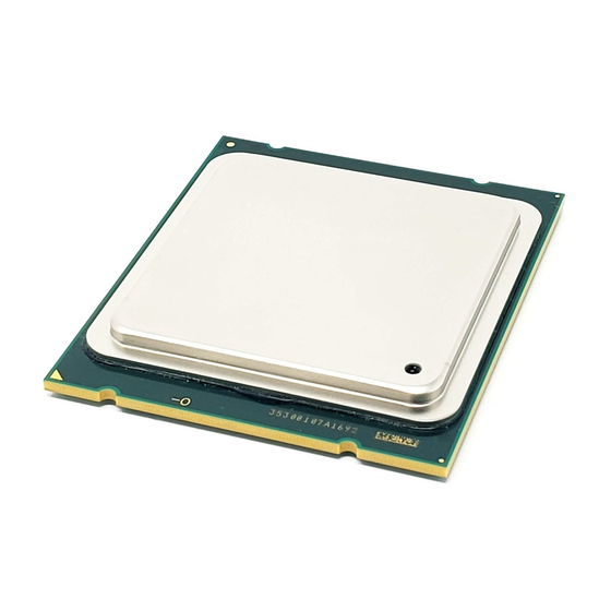
Specifications Package Mechanical Specifications ® ® The Intel Core™ i7-3960X, i7-3970X processor Extreme Edition, Intel Core™ i7- ® 3930K processor, and Intel Core™ i7-3820 processor are packaged in a 2011-land Flip-Chip Land Grid Array package that interfaces with the baseboard using the LGA2011-0 socket. -
Page 16: Package Mechanical Drawing
Package Mechanical Specifications 2.1.1 Package Mechanical Drawing Figure 2-2 shows the basic package layout and dimensions. The detailed package mechanical drawings are in Appendix D. The drawings include dimensions necessary to design a thermal solution for the processor. These dimensions include: 1. -
Page 17: Package Loading Specifications
Package Mechanical Specifications 2.1.3 Package Loading Specifications Table 2-1 provides load specifications for the processor package. These maximum limits should not be exceeded during heatsink assembly, shipping conditions, or standard use condition. Exceeding these limits during test may result in component failure. -
Page 18: Processor Materials
This diagram is to aid in the identification of the processor. Figure 2-3. Processor Top-Side Markings Legend: Sample (QDF): GRP1LINE1: i{M}{C}YY GRP1LINE2: INTEL CONFIDENTIAL GRP1LINE3: QDF ES SPEED GRP1LINE4: XXXXX GRP1LINE5: {FPO} {e4} GRP1LINE1... -
Page 19: Lga2011-0 Socket
LGA2011-0 Socket LGA2011-0 Socket This chapter describes a surface mount, LGA (Land Grid Array) socket intended for the processors in the Platform. The socket provides I/O, power and ground contacts. The socket contains 2011 contacts arrayed about a cavity in the center of the socket with lead-free solder balls for surface mounting on the motherboard. -
Page 20: Contact Wiping Direction
LGA2011-0 Socket Figure 3-2. Contact Wiping Direction Contact Wiping Direction Contact Wiping Direction Contact Wiping Direction The socket must be compatible with the package (processor) and the Independent Loading Mechanism (ILM). The design includes a back plate that is integral to having a uniform load on the socket solder joints and the contacts. -
Page 21: Lga2011-0 Socket Contact Numbering (Top View Of Socket)
LGA2011-0 Socket Figure 3-4. LGA2011-0 Socket Contact Numbering (Top View of Socket) Thermal/Mechanical Specifications and Design Guide... -
Page 22: Contact/Land Mating Location
LGA2011-0 Socket Contact/Land Mating Location All socket contacts are designed such that the contact tip lands within the substrate pad boundary before any actuation load is applied and remain within the pad boundary at final installation, after actuation load is applied. The offset between LGA land center and solder ball center is defined in Figure 3-5. -
Page 23: Attachment To Motherboard
LGA2011-0 Socket Figure 3-6. LGA2011-0 Socket Land Pattern (Top View of Board) Attachment to Motherboard The socket is attached to the motherboard by 2011 solder balls. There are no additional external methods (that is, screw, extra solder, adhesive, and so forth) to attach the socket. -
Page 24: Socket Components
LGA2011-0 Socket Socket Components The socket has two main components, the socket body and Pick and Place (PnP) cover, and is delivered as a single integral assembly. Refer to Appendix B for detailed drawings. 3.4.1 Socket Body Housing The housing material is thermoplastic or equivalent with UL 94 V-0 flame rating capable of withstanding 260 °C for 40 seconds (typical reflow/rework). -
Page 25: Lga2011-0 Pick And Place Cover
3-8, the pick and place (PnP) cover remains on the socket during ILM installation. Once the ILM with its cover is installed, Intel is recommending the PnP cover be removed to help prevent damage to the socket contacts. To reduce the risk of bent contacts the PnP Cover and ILM Cover were designed to not be compatible. -
Page 26: Socket Standoffs And Package Seating Plane
LGA2011-0 Socket 3.4.5 Socket Standoffs and Package Seating Plane Standoffs on the bottom of the socket base establish the minimum socket height after solder reflow and are specified in Appendix Similarly, a seating plane on the topside of the socket establishes the minimum package height. -
Page 27: Independent Loading Mechanism (Ilm)
ILM as a system. These studies directly impact the design of the ILM. The Intel reference ILM will be “built to print” from Intel controlled drawings. Intel recommends using the Intel Reference ILM. Custom non-Intel ILM designs do not benefit from Intel's detailed studies and may not incorporate critical design parameters. -
Page 28: Square Ilm Design Concept
Independent Loading Mechanism (ILM) Square ILM Design Concept The square ILM consists of two assemblies that will be procured as a set from the enabled vendors. These two components are the ILM assembly and back plate. 4.1.1 Square ILM Assembly Design Overview Figure 4-1. -
Page 29: Ilm As Universal Retention Mechanism
Independent Loading Mechanism (ILM) The hinge lever and active lever are designed to place equal force on both ends of the ILM load plate. The frame provides the hinge locations for the levers. The hinge lever connects the load plate to the frame. When closed, the load plate applies four point loads onto the IHS at the “finger”... -
Page 30: Ilm Features
Independent Loading Mechanism (ILM) ILM Features • Allows for topside thermal solution attach to a rigid structure. This eliminates the motherboard thickness dependency from the mechanical stackup. • Captive nuts clamp the ILM frame to the board and reduced board bending leading to higher solder joint reliability. -
Page 31: Ilm Opening Sequence
Independent Loading Mechanism (ILM) Figure 4-5. ILM Lever Closing Sequence Step 1 Close Active Lever Step 2 Step 2 Close Hinge Lever ILM lever closing sequence is shown in Figure 4-5. 1. Latch Active Lever first. 2. Close Hinge Lever second. Note: The ILM closing sequence is marked on the ILM load plate. -
Page 32: Opening Ilm
Independent Loading Mechanism (ILM) Figure 4-6. Opening ILM Step 1 Open Hinge Lever Opening the hinge lever provides the clearance to open the active lever Step 2 Open Active Lever The ILM opening sequence is shown in Figure 4-6. 1. Open hinge lever 2. -
Page 33: Ilm Keying
Independent Loading Mechanism (ILM) 4.2.2.1 ILM Keying As indicated in Figure 4-8, the socket protrusion and ILM key features prevent 180- degree rotation of ILM assembly with respect to socket. This result in a specific orientation with respect to ILM active lever and pin 1 of the socket body. Figure 4-8. -
Page 34: Ilm Assembly
1. Using SMT, mount the socket onto the circuit board. Intel provides detailed instruction for lead free manufacturing of complex interconnects on the Intel Learning Network (http://iln.intel.com/Portal/Scripts/Home/Home.aspx). -
Page 35: Processor Installation
Independent Loading Mechanism (ILM) Processor Installation The hinge lever can be locked down to keep it out of the way when removing the PnP cover and installing the processor (Figure 4-11). If the hinge lever is locked down when the ILM is open, then the load plate will be locked in the open position and less likely to fall closed if bumped. -
Page 36: Ilm Cover
3. Close the Hinge lever with a smooth uniform motion and latch to the ILM. ILM Cover Intel has developed a cover that will snap on to the ILM for the LGA2011 socket family. The ILM cover is intended to reduce the potential for socket contact damage from the operator / customer fingers being close to the socket contacts to remove or install the pick and place cover. -
Page 37: Heatsink To Ilm Interface
UL 60950-1. Figure 4-14. ILM with Cover Note: Intel recommends removing the Pick and Place cover (PnP) of the socket body in manufacturing as soon as possible at the time when ILM is being installed. Heatsink to ILM interface Heatsinks for processors in the LGA2011-0 socket attach directly to the ILM using M4 fasteners. -
Page 38: Heatsink To Ilm Interface
Independent Loading Mechanism (ILM) Figure 4-15. Heatsink to ILM Interface 80.00 38.00 80.00 38.00 M4x0.7 4 PL 4.178 +0.38/ -0.20 See Note Below Note: For IHS height above board see Table 5-2. § Thermal/Mechanical Specifications and Design Guide... -
Page 39: Lga2011-0 Socket And Ilm Electrical, Mechanical, And Environmental Specifications
LGA2011-0 Socket and ILM Electrical, Mechanical, and Environmental Specifications LGA2011-0 Socket and ILM Electrical, Mechanical, and Environmental Specifications This chapter describes the electrical, mechanical, and environmental specifications for the LGA2011-0 socket and the Independent Loading Mechanism. Component Mass Table 5-1. Socket and Retention Component Mass Component Mass... -
Page 40: Loading Specifications
LGA2011-0 Socket and ILM Electrical, Mechanical, and Environmental Specifications Loading Specifications The socket will be tested against the conditions listed in Chapter 9, “Quality and Reliability Requirements” with heatsink and the ILM attached, under the loading conditions outlined in this chapter. Table 5-3 provides load specifications for the LGA2011-0 socket with the ILM installed. -
Page 41: Environmental Requirements
Freeze stressing Perform stressing to requirements and perform validate accelerated additional data turns stressing assumptions and determine acceleration factors A detailed description of this methodology can be found at: ftp://download.intel.com/technology/itj/q32000/pdf/reliability.pdf § Thermal/Mechanical Specifications and Design Guide... - Page 42 LGA2011-0 Socket and ILM Electrical, Mechanical, and Environmental Specifications Thermal/Mechanical Specifications and Design Guide...
-
Page 43: Thermal Management Specifications
The boxed processor will ship with a component thermal solution. 6.1.1 Thermal Specifications To allow optimal operation and long-term reliability of Intel processor-based systems, the processor must remain within the minimum and maximum case temperature ) specifications as defined by the applicable thermal profile. Thermal solutions... -
Page 44: And Dts Based Thermal Specifications
ICC. Refer to the electrical loadline specifications in CC_MAX ® ® the Datasheet. The Intel Core™ i7-3960X, i7-3970X processor Extreme Edition, Intel Core™ i7-3930K ® processor, and Intel Core™ i7-3820 processor may be delivered under multiple VIDs for each frequency. -
Page 45: Ttv Thermal Profile
Thermal Management Specifications Figure 6-1. TTV Thermal Profile Notes: Refer to Table 6-2 for discrete points that constitute thermal profile. Refer to the Chapter 8 for system and environmental implementation details. Table 6-2. 130W TTV Thermal Profile (Sheet 1 of 2) Power (W) Maximum TTV Power (W) -
Page 46: Processor Specification For Operation Where Digital Thermal Sensor Exceeds Tcontrol
Table 6-3 for the Intel Core™ i7-3960X, i7-3970X ® ® processor Extreme Edition, Intel Core™ i7-3930K processor, and Intel Core™ i7- 3820 processor. To get the full acoustic benefit of the DTS specification, ambient temperature monitoring is necessary. ® Table 6-3. -
Page 47: Thermal Metrology
® Table 6-3. Thermal Solution Performance above T for the Intel Core™ i7-3960X, CONTROL ® i7-3970X Processor Extreme Edition, Intel Core™ i7-3930K Processor, and ® Intel Core™ i7-3820 Processor (Sheet 2 of 2) AMBIENT DTS = T DTS = -1 CONTROL 29.0... -
Page 48: Processor Core Thermal Features
Thermal Management Specifications Processor Core Thermal Features 6.2.1 Processor Temperature A feature in the processor is a software readable field in the IA32_TEMPERATURE_TARGET register that contains the minimum temperature at which the TCC will be activated and PROCHOT_N will be asserted. The TCC activation temperature is calibrated on a part-by-part basis and normal factory variation may result in the actual TCC activation temperature being higher than the value listed in the register. -
Page 49: Frequency/Svid Control
Thermal Management Specifications 6.2.2.1 Frequency/SVID Control The processor uses Frequency/SVID control whereby TCC activation causes the processor to adjust its operating frequency (using the core ratio multiplier) and input voltage (using the SVID signals). This combination of reduced frequency and voltage results in a reduction to the processor power consumption. -
Page 50: Clock Modulation
Thermal Management Specifications 6.2.2.2 Clock Modulation Clock modulation is performed by alternately turning the clocks off and on at a duty cycle specific to the processor (factory configured to 37.5% on and 62.5% off for TM1). The period of the duty cycle is configured to 32 microseconds when the TCC is active. Cycle times are independent of processor frequency. -
Page 51: Thermtrip_N Signal
In this way, it is highly flexible even though underlying logic is simple. The interface design was optimized for interfacing to Intel processor and chipset components in both single processor and multiple processor environments. The single wire interface provides low board routing overhead for the multiple load connections in the congested routing area near the processor and chipset components. -
Page 52: Peci Client Capabilities
PECI command details. 6.3.2 PECI Client Capabilities ® ® The Intel Core™ i7-3960X, i7-3970X processor Extreme Edition, Intel Core™ i7- ® 3930K processor, and Intel Core™ i7-3820 processor support the following sideband functions: • Processor and DRAM thermal management •... -
Page 53: Peci Interface
In this way, it is highly flexible even though underlying logic is simple. The interface design was optimized for interfacing to Intel processor and chipset components in both single processor and multiple processor environments. The single wire interface provides low board routing overhead for the multiple load connections in the congested routing area near the processor and chipset components. -
Page 54: Peci Client Capabilities
® processor, and Intel Core™ i7-3820 processor Intel Interconnect Built-In Self Test (Intel IBIST) allows for in-field diagnostic capabilities in memory controller interfaces. PECI provides a port to execute these diagnostics using its PCI Configuration read and write capabilities. Thermal/Mechanical Specifications and Design Guide... -
Page 55: Client Command Suite
PECI Interface 7.1.2 Client Command Suite Each PECI command requires at least one frame check sequence (FCS) byte to ensure reliable data exchange between originator and client. The PECI message protocol defines two FCS bytes that are returned by the client to the message originator. The first FCS byte covers the client address byte, the Read and Write Length bytes, and all bytes in the write data block. -
Page 56: Getdib()
PECI Interface 7.1.2.2 GetDIB() The processor PECI client implementation of GetDIB() includes an 8-byte response and provides information regarding client revision number and the number of supported domains. All processor PECI clients support the GetDIB() command. 7.1.2.2.1 Command Format The GetDIB() format is as follows: Write Length: 0x01 Read Length: 0x08 Command: 0xF7... -
Page 57: Revision Number Definition
PECI Interface 7.1.2.2.3 Revision Number All clients that support the GetDIB command also support Revision Number reporting. The revision number may be used by a host or originator to manage different command suites or response codes from the client. Revision Number is always reported in the second byte of the GetDIB() response. -
Page 58: Gettemp()
PECI Interface 7.1.2.3 GetTemp() The GetTemp() command is used to retrieve the maximum die temperature from a target PECI address. The temperature is used by the external thermal management system to regulate the temperature on the die. The data is returned as a negative value representing the number of degrees centigrade below the maximum processor junction temperature (T ). -
Page 59: Rdpkgconfig()
PECI Interface 7.1.2.3.2 Supported Responses The typical client response is a passing FCS and valid thermal data. Under some conditions, the client’s response will indicate a failure. GetTemp() response definitions are listed in Table 7-3. Refer to Section 7.1.9.3 for more details on sensor errors. Table 7-3. -
Page 60: Rdpkgconfig() Response Definition
PECI Interface Figure 7-8. RdPkgConfig() Byte # Write Length Read Length Cmd Code Client Address Byte 0x05 {0x02, 0x03, 0x05} 0xa1 Definition Host ID[7:1] & Index Parameter Retry[0] Completion Data (1, 2 or 4 bytes) Code Note: The 2-byte parameter field and 4-byte read data field defined in Figure 7-8 are sent in standard PECI ordering with LSB first and MSB last. -
Page 61: Wrpkgconfig()
PECI Interface 7.1.2.5 WrPkgConfig() The WrPkgConfig() command provides write access to the package configuration space (PCS) within the processor, including various power and thermal management functions. Typical PCS write services supported by the processor may include power limiting, thermal averaging constant programming and so on. Refer to Section 7.1.2.6 for more details on processor-specific services supported through this command. -
Page 62: Package Configuration Capabilities
PECI Interface 7.1.2.5.2 Supported Responses The typical client response is a passing FCS, a passing Completion Code and valid data. Under some conditions, the client’s response will indicate a failure. Table 7-5. WrPkgConfig() Response Definition Response Meaning Bad Write FCS Electrical error or AW FCS failure Abort FCS Invalid command formatting (mismatched RL/WL/Command Code) -
Page 63: Rdpkgconfig() & Wrpkgconfig() Dram Thermal Services Summary
PECI Interface Table 7-6. RdPkgConfig() & WrPkgConfig() DRAM Thermal Services Summary Parameter RdPkgConfig() WrPkgConfig() Decimal Index Value Data Data Service Description Value (word) (dword) (dword) (byte) DRAM Thermal Read the DRAM Thermal DRAM Thermal Estimation Estimation configuration 0x0000 Estimation Configu- Configuration parameters. -
Page 64: Dram Thermal Estimation Configuration Data
PECI Interface 7.1.2.6.2 DRAM Thermal Estimation Configuration Data Read/Write This feature is relevant only when activity-based DRAM temperature estimation methods are being utilized and would apply to all the DIMMs on all the memory channels. The write allows the PECI host to configure the ‘ ’ and ‘ ’ variables in Figure 7-10 for DRAM channel temperature filtering as per the equation below: Energy... -
Page 65: Dram Rank Temperature Write Data
PECI Interface Figure 7-11. DRAM Rank Temperature Write Data Rank# 3 Rank# 2 Rank# 1 Rank# 0 Absolute Temp Absolute Temp Absolute Temp Absolute Temp (in Degrees C) (in Degrees C) (in Degrees C) (in Degrees C) Rank Temperature Data Reserved DIMM Index Channel Index... -
Page 66: Ambient Temperature Reference Data
PECI Interface Figure 7-13. Ambient Temperature Reference Data Ambient Reserved Temperature (in Degrees C) Ambient Temperature Reference Data 7.1.2.6.6 DRAM Channel Temperature Read This feature enables a PECI host read of the maximum temperature of each channel. This would include all the DIMMs within the channel and all the ranks with each of the DIMMs. -
Page 67: Dram Power Info Read Data
PECI Interface 7.1.2.6.8 DRAM Power Info Read This read returns the minimum, typical and maximum DRAM power settings and the maximum time window over which the power can be sustained for the entire DRAM domain and is inclusive of all the DIMMs within all the memory channels. Any power values specified by the power limiting entity that is outside of the range specified through these settings cannot be guaranteed. -
Page 68: Processor Thermal And Power Optimization Capabilities
PECI Interface Figure 7-18. DRAM Power Limit Performance Data Accumulated DRAM Throttle Time DRAM Power Limit Performance 7.1.2.7 Processor Thermal and Power Optimization Capabilities Table 7-8. RdPkgConfig() & WrPkgConfig() Processor Thermal and Power Optimization Services Summary (Sheet 1 of 3) Parameter RdPkgConfig() WrPkgConfig() - Page 69 PECI Interface Table 7-8. RdPkgConfig() & WrPkgConfig() Processor Thermal and Power Optimization Services Summary (Sheet 2 of 3) Parameter RdPkgConfig() WrPkgConfig() Index Value Data Data Service Value Description (word) (dword) (dword) (byte) Read the thermal status register and optionally clear any log bits. Package Thermal The register includes status and Thermal Status...
- Page 70 PECI Interface Table 7-8. RdPkgConfig() & WrPkgConfig() Processor Thermal and Power Optimization Services Summary (Sheet 3 of 3) Parameter RdPkgConfig() WrPkgConfig() Index Value Data Data Service Value Description (word) (dword) (dword) (byte) Socket Number of retired Read retired instruction count for Performance 0x0000 instructions per time...
-
Page 71: Cpuid Data
Platform ID Data • Uncore Device ID: This information can be used to uniquely identify the processor device when combined with the Vendor Identification register content. Refer to the ® appropriate register description for the exact Intel Core™ i7-3960X, i7-3970X ® ®... -
Page 72: Uncore Device Id
PECI Interface • Max Thread ID: The maximum Thread ID data provides the number of supported Figure 7-21. Uncore Device ID RESERVED Uncore Device ID Uncore Device ID Data processor threads. Note that this value is dependent on the number of cores within the processor as determined by the processor SKU and is independent of whether certain cores or corresponding threads are enabled or disabled. -
Page 73: Package Power Sku Data
PECI Interface Table 7-10. Power Control Register Unit Calculations Unit Field Value Calculation Default Value TIME UNIT Time 1s / 2 1s / 2 = 976 µs ENERGY UNIT Energy 1J / 2 1J / 2 = 15.3 µJ POWER UNIT Power 1W / 2 1W / 2... -
Page 74: Package Temperature Read Data
PECI Interface 7.1.2.7.6 Package Temperature Read This read returns the maximum processor die temperature in 16-bit PECI format. The upper 16 bits of the response data are reserved. Figure 7-26. Package Temperature Read Data Sign PECI Temperature PECI Temperature RESERVED (Integer Value) (Fractional Value) PACKAGE_TEMPERATURE MSR... -
Page 75: Per Core Temperature Read
PECI Interface Figure 7-28. Thermal Status Word 6 5 4 3 2 1 0 Reserved Critical Temperature Log Critical Temperature Status Bidirectional PROCHOT# Log Bidirectional PROCHOT# Status TCC Activation Log TCC Activation Status 7.1.2.7.9 Thermal Averaging Constant Write / Read This feature allows the PECI host to control the window over which the estimated processor PECI temperature is filtered. -
Page 76: Acpi P-T Notify Read/Write
PECI Interface 7.1.4 ACPI P-T Notify Read/Write This interface coupled with limiting OSPM usage of P-States using ACPI _PPC object and programming of the package power limit registers enables turbo capability while limiting maximum package power dissipation to be within the specified package power limit. -
Page 77: Power Limit For The V
PECI Interface 7.1.4.4 Power Limit for the V Power Plane Write / Read This feature allows the PECI host to program the power limit over a specified time or control window for the V power plane. Actual values are chosen based on the VR (voltage regulator) capabilities. -
Page 78: Socket Power Limit Performance Status Read
PECI Interface 7.1.4.6 Socket Power Limit Performance Status Read This service allows the PECI host to assess the performance impact of the currently active power limiting modes. The read return data contains the total amount of time for which the entire processor package has been operating in a power state that is lower than what the operating system originally requested. -
Page 79: Rdiamsr()
PECI Interface 7.1.4.9 RdIAMSR() The RdIAMSR() PECI command provides read access to Model Specific Registers (MSRs) defined in the processor’s Intel Architecture (IA). Refer to Table 7-12 for the ® ® exact listing of Intel Core™ i7-3960X, i7-3970X processor Extreme Edition, Intel ®... -
Page 80: Processor Id Construction Example
PECI Interface Figure 7-37. Processor ID Construction Example Figure 7-38. RdIAMSR() Byte # Write Length Read Length Cmd Code Byte Client Address <Process Name> 0x05 {0x02, 0x03, 0x05, 0x09) 0xb1 Definition Host ID[7:1] & Processor ID MSR Address Retry[0] Completion Data (1, 2, 4 or 8 bytes) Code Data (1, 2, 4 or 8 bytes) -
Page 81: Rdiamsr() Response Definition
PECI Interface 7.1.4.9.3 Supported Responses The typical client response is a passing FCS, a passing Completion Code and valid data. Under some conditions, the client’s response will indicate a failure. Table 7-11. RdIAMSR() Response Definition Response Meaning Bad FCS Electrical error Abort FCS Invalid command formatting (mismatched RL/WL/Command Code) CC: 0x40... -
Page 82: Rdpciconfig()
The exact listing of supported devices, functions and registers can be found in the relevant sections of the ® Intel Core™ i7 Processor Family for the LGA-2011 Socket Datasheet, Volume 2. PECI originators may conduct a device/function/register enumeration sweep of this space by issuing reads in the same manner that the BIOS would. -
Page 83: Rdpciconfig() Response Definition
PECI Interface PCI configuration reads may be issued in byte, word or dword granularities. 7.1.4.10.1 Command Format The RdPCIConfig() format is as follows: Write Length: 0x06 Read Length: 0x05 (dword) Command: 0x61 Description: Returns the data maintained in the PCI configuration space at the requested PCI configuration address. -
Page 84: Rdpciconfiglocal()
The exact listing of supported ® devices, functions and registers can be found in the relevant sections of the Intel Core™ i7 Processor Family for the LGA-2011 Socket Datasheet, Volume 2. PECI originators may conduct a device/function/register enumeration sweep of this space by issuing reads in the same manner that the BIOS would. -
Page 85: Rdpciconfiglocal() Response Definition
PECI Interface 7.1.4.11.1 Command Format The RdPCIConfigLocal() format is as follows: Write Length: 0x05 Read Length: 0x02 (byte), 0x03 (word), 0x05 (dword) Command: 0xe1 Description: Returns the data maintained in the PCI configuration space within the processor at the requested PCI configuration address. The Read Length dictates the desired data return size. -
Page 86: Wrpciconfiglocal()
PECI Interface Table 7-14. RdPCIConfigLocal() Response Definition (Sheet 2 of 2) Response Meaning Response timeout. The processor is not able to allocate resources for servicing this CC: 0x81 command at this time. Retry is appropriate. The processor hardware resources required to service this command are in a low power CC: 0x82 state. -
Page 87: Wrpciconfiglocal() Response Definition
PECI Interface Figure 7-43. WrPCIConfigLocal() Byte # Write Length Read Length Cmd Code Client Address Byte {0x07, 0x08, 0x0a} 0x01 0xe5 Definition Host ID[7:1] & PCI Configuration Address Retry[0] Data (1, 2 or 4 bytes) Completion AW FCS Code The 3-byte PCI configuration address and write data field defined in Figure 7-43 sent in standard PECI ordering with LSB first and MSB last. -
Page 88: Client Management
Core™ i7 Processor Family for the LGA-2011 Socket Datasheet, Volume 2 for more details on specific register definitions. It also enables writing to processor REUT (Robust Electrical Unified Test) registers associated with the Intel® QPI, PCIe* and DDR3 functions. Table 7-16. WrPCIConfigLocal() Memory Controller Device/Function Support Device... -
Page 89: Device Discovery
PECI client will also be tri-stated. Processor tri-state controls are described in the relevant sections of the Datasheet listed in Table 1-1. ® ® Figure 7-44. Intel Core™ i7-3960X, i7-3970X Processor Extreme Edition, Intel Core™ i7- ® 3930K Processor, and Intel Core™ i7-3820 Processor PECI Power-up Timeline() PWRGOOD... -
Page 90: C-States
PECI Interface 7.1.5.4 C-states The processor PECI client may be fully functional in most core and package C-states. • The Ping(), GetDIB(), GetTemp(), RdPkgConfig() and WrPkgConfig() commands have no measurable impact on processor power in any of the core or package C- states. -
Page 91: Processor Reset
PECI Interface 7.1.5.6 Processor Reset The processor PECI client is fully reset on all RESET_N assertions. Upon deassertion of RESET_N where power is maintained to the processor (otherwise known as a ‘warm reset’), the following are true: • The PECI client assumes a bus Idle state. •... -
Page 92: Originator Retry And Timeout Policy
7.1.6 Multi-Domain Commands ® ® The Intel Core™ i7-3960X, i7-3970X processor Extreme Edition, Intel Core™ i7- ® 3930K processor, and Intel Core™ i7-3820 processor does not support multiple domains, but it is possible that future products will, and the following tables are included as a reference for domain-specific definitions. -
Page 93: Client Responses
PECI Interface Table 7-21. Multi-Domain Command Code Reference Domain 0 Domain 1 Command Name Code Code GetTemp() 0x01 0x02 RdPkgConfig() 0xa1 0xa2 WrPkgConfig() 0xa5 0xa6 RdIAMSR() 0xb1 0xb2 RdPCIConfig() 0x61 0x62 WrPCIConfig() 0x65 0x66 RdPCIConfigLocal() 0xe1 0xe2 WrPCIConfigLocal() 0xe5 0xe6 7.1.7 Client Responses 7.1.7.1... -
Page 94: Originator Responses
PECI Interface Table 7-23. Device Specific Completion Code (CC) Definition Completion Description Code 0x40 Command Passed Response timeout. The processor was not able to generate the required response in a timely CC: 0x80 fashion. Retry is appropriate. Response timeout. The processor was not able to allocate resources for servicing this CC: 0x81 command. -
Page 95: Dts Temperature Data
PECI Interface 7.1.9 DTS Temperature Data 7.1.9.1 Format The temperature is formatted in a 16-bit, 2’s complement value representing a number of 1/64 degrees centigrade. This format allows temperatures in a range of ±512 °C to be reported to approximately a 0.016 °C resolution. Figure 7-45. -
Page 96: Reserved Values
PECI Interface 7.1.9.3 Reserved Values Several values well out of the operational range are reserved to signal temperature sensor errors. These are summarized in Table 7-25. Table 7-25. Error Codes and Descriptions Error Code Description 0x8000 General Sensor Error (GSE) 0x8001 Reserved Sensor is operational, but has detected a temperature below its operational range... -
Page 97: Thermal Solutions
This section describes the desktop reference heatsink, design targets for a radial fin heatsink (DHR-A) and a tall heat pipe heatsink (T-HPHS) and thermal design guidelines ® ® for the Intel Core™ i7-3960X, i7-3970X processor Extreme Edition, Intel Core™ i7- ® 3930K processor, and Intel Core™ i7-3820 processor. -
Page 98: Assembly Process For Reference Heatsinks
Thermal Solutions Figure 8-2. Tall Heat Pipe Heatsink Assembly Assembly Process for Reference Heatsinks Unless noted the assembly process covers both the radial fin and Tall Heat Pipe Heat Sink (T-HPHS). Compliance to Board Keepout Zones in Appendix A is assumed for this assembly process. -
Page 99: Geometric Envelope For The Intel® Reference Atx Thermal Mechanical Design
Thermal Solutions ® Geometric Envelope for the Intel Reference ATX Thermal Mechanical Design Figure 8-3 shows a 3-D representation of the board component keep out for the reference ATX thermal solution. A fully dimensioned drawing of the keepout information is available at... -
Page 100: Structural Considerations
LGA2011 socket ILM. Thermal Interface Material A thermal interface material (TIM) provides conductivity between the IHS and heat sink. ® Table 8-3. Intel Reference Thermal Solution TIM Thermal Solution T-HPHS SHIN-ETSU G751 (reference) Tower (Cu/Al and Heatpipe) DOW TC-1996 (collaboration) -
Page 101: Tall Heat Pipe Heat Sink Performance
Thermal Solutions Tall Heat Pipe Heat Sink Performance Intel has completed the initial engineering validation for the T-HPHS. The following two figures show the Psi-ca versus RPM Figure 8-4 and Sound Power (BA) versus RPM Figure 8-5. Figure 8-4. T-HPHS Psi-ca versus RPM Notes: The target Psi-ca of 0.199 °C / W is at approximately 1800 RPM... -
Page 102: Thermal Design Guidelines
Intel Turbo Boost 2 Technology Intel Turbo Boost 2 Technology is a feature available on certain processor SKUs that opportunistically, and automatically, allows the processor to run faster than the marked frequency if the part is operating below its power, temperature and current limits. -
Page 103: Fan Speed Control
Thermal Solutions Figure 8-6. Processor Thermal Characterization Parameter Relationships 8.8.3 Fan Speed Control When DTS (Digital Thermal Sensor) value is less than T , the thermal profile can CONTROL be ignored. The DTS value is a relative temperature to PROCHOT, which is the maximum allowable temperature before the thermal control circuit is activated. - Page 104 Thermal Solutions Thermal/Mechanical Specifications and Design Guide...
-
Page 105: Quality And Reliability Requirements
Quality and Reliability Requirements Quality and Reliability Requirements Use Conditions Intel evaluates reliability performance based on the use conditions (operating environment) of the end product by using acceleration models. The use condition environment definitions provided in Table 9-1 Table 9-2 based on speculative use condition assumptions, and are provided as examples only. -
Page 106: Intel ® Reference Component Validation
® Intel Reference Component Validation Intel tests reference components individually and as an assembly on mechanical test boards and assesses performance to the envelopes specified in previous sections by varying boundary conditions. While component validation shows a reference design is tenable for a limited range of conditions, customers need to assess their specific boundary conditions and perform reliability testing based on their use conditions. -
Page 107: Post-Test Pass Criteria Examples
• All enabling components, including socket and thermal solution parts. The pass criterion is that the system under test shall successfully complete the checking of BIOS, basic processor functions and memory, without any errors. Intel PC Diags is an example of software that can be utilized for this test. - Page 108 Halogen flame retardant free (HFR-Free) PCB: In future revisionsof this document, Intel will be providing guidance on the mechanical impact to using a HFR- free laminate in the PCB. Lead-free and Pb-free: Lead has not been intentionally added, but lead may still exist as an impurity below 1000 ppm.
-
Page 109: A Mechanical Drawings
Mechanical Drawings Mechanical Drawings Table A-1 lists the Mechanical drawings included in this appendix. Table A-1. Mechanical Drawing List Description Figure Board Keepin / Keepout Zones (Sheet 1 of 2) Figure A-1 Board Keepin / Keepout Zones (Sheet 2 of 2) Figure A-2 Thermal/Mechanical Specifications and Design Guide... -
Page 110: Board Keepin / Keepout Zones (Sheet 1 Of 2)
Mechanical Drawings Figure A-1. Board Keepin / Keepout Zones (Sheet 1 of 2) 52.00 49.99 48.20 42.00 40.52 40.00 39.45 34.18 34.57 23.00 25.57 23.00 ) 7.00 0.00 ) 7.00 23.00 25.57 23.00 34.57 34.18 39.45 40.00 40.52 42.00 48.20 49.99 52.00 Thermal/Mechanical Specifications and Design Guide... -
Page 111: Board Keepin / Keepout Zones (Sheet 2 Of 2)
Mechanical Drawings Figure A-2. Board Keepin / Keepout Zones (Sheet 2 of 2) 52.00 41.00 40.00 34.60 31.50 26.50 11.19 0.00 11.19 26.50 31.50 34.60 40.00 41.00 52.00 § Thermal/Mechanical Specifications and Design Guide... - Page 112 Mechanical Drawings Thermal/Mechanical Specifications and Design Guide...
-
Page 113: B Socket Mechanical Drawings
Socket Mechanical Drawings Socket Mechanical Drawings Table B-1 lists the socket drawings included in this appendix. Table B-1. Socket Drawing List Drawing Description Figure Number Socket Mechanical Drawing (Sheet 1 of 4) Figure B-1 Socket Mechanical Drawing (Sheet 2 of 4) Figure B-2 Socket Mechanical Drawing (Sheet 3 of 4) Figure B-3... -
Page 114: Socket Mechanical Drawing (Sheet 1 Of 4)
Socket Mechanical Drawings Figure B-1. Socket Mechanical Drawing (Sheet 1 of 4) Thermal/Mechanical Specifications and Design Guide... -
Page 115: Socket Mechanical Drawing (Sheet 2 Of 4)
Socket Mechanical Drawings Figure B-2. Socket Mechanical Drawing (Sheet 2 of 4) Thermal/Mechanical Specifications and Design Guide... -
Page 116: Socket Mechanical Drawing (Sheet 3 Of 4)
Socket Mechanical Drawings Figure B-3. Socket Mechanical Drawing (Sheet 3 of 4) Thermal/Mechanical Specifications and Design Guide... -
Page 117: Socket Mechanical Drawing (Sheet 4 Of 4)
Socket Mechanical Drawings Figure B-4. Socket Mechanical Drawing (Sheet 4 of 4) § Thermal/Mechanical Specifications and Design Guide... - Page 118 Socket Mechanical Drawings Thermal/Mechanical Specifications and Design Guide...
-
Page 119: C Component Suppliers
A. Mechanical models of the keep in zone and socket are listed in Table 1-1. ® C.1.1 Intel Reference or Collaboration Thermal Solutions Customers can purchase the Intel reference or collaboration thermal solutions from the suppliers listed in Table C-1 Table C-2. ® Table C-1. Suppliers for the Intel Reference Thermal Solutions ®... -
Page 120: Suppliers For The Lga2011-0 Socket And Ilm
Socket mechanical drawings are provided in Appendix A. Mechanical models are listed in Table 1-1. Table C-2. Suppliers for the LGA2011-0 Socket and ILM Foxconn ® Item Intel Amtek Lotes (Hon Hai) LGA2011-0 PE201127-4351- E64556-002 None Socket LGA2011-0 ILM PT44L41-4411... -
Page 121: D Package Mechanical Drawings
Package Mechanical Drawings Package Mechanical Drawings Table D-1 lists the mechanical drawings included in this appendix. Table D-1. Mechanical Drawing List Drawing Description Figure Number Processor Package Drawing (Sheet 1 of 2) Figure D-1 Processor Package Drawing (Sheet 2of 2) Figure D-2 Thermal/Mechanical Specifications and Design Guide... -
Page 122: Processor Package Drawing (Sheet 1 Of 2)
Package Mechanical Drawings Figure D-1. Processor Package Drawing (Sheet 1 of 2) Thermal/Mechanical Specifications and Design Guide... -
Page 123: Processor Package Drawing (Sheet 2Of 2)
Package Mechanical Drawings Figure D-2. Processor Package Drawing (Sheet 2of 2) § Thermal/Mechanical Specifications and Design Guide... - Page 124 Package Mechanical Drawings Thermal/Mechanical Specifications and Design Guide...