Sign In
Upload
Manuals
Brands
Infineon Manuals
Microcontrollers
XMC4000 series
Infineon XMC4000 series Microcontroller Manuals
Manuals and User Guides for Infineon XMC4000 series Microcontroller. We have
12
Infineon XMC4000 series Microcontroller manuals available for free PDF download: Reference Manual, Application Manual, Device Manual, Board User's Manual, User Manual
Infineon XMC4000 series Reference Manual (2689 pages)
ARM Cortex-M4 32-bit processor core
Brand:
Infineon
| Category:
Microcontrollers
| Size: 18.85 MB
Table of Contents
Table of Contents
8
Table 6-5 Table
8
Table 7-2 Table
8
Table 7-4 Table
9
Table 8-1 Table
10
Table 8-3 Table
11
Table 8-5 Table
12
Table 8-7 Table
13
Table 8-9 Table
14
Table 8-11 Table
15
Table 9-2 Table
16
Table 9-4 Table
17
Table 10-2 Table
18
Table 10-4 Table
19
Table 11-2 Table
20
Table 11-6 Table
21
Table 12-1 Table
22
Table 12-3 Table
23
Table 12-5 Table
24
Table 12-7 Table
25
Table 12-9 Table
26
Table 13-2 Table
27
Table 13-6 Table
28
Table 16-1 Table
32
Table 16-3 Table
33
Table 16-5 Table
34
Table 16-7 Table
35
Table 17-1 Table
36
Table 17-3 Table
37
Table 17-5 Table
38
Table 17-7 Table
39
Introduction
48
Introduction
49
Overview
49
Block Diagram
51
CPU Subsystem
52
On-Chip Memories
53
Communication Peripherals
54
Analog Frontend Peripherals
56
Industrial Control Peripherals
57
On-Chip Debug Support
57
Central Processing Unit (CPU)
60
Overview
60
Features
61
Block Diagram
61
Programmers Model
63
Processor Mode and Privilege Levels for Software Execution
63
Stacks
63
Table 6-3 Table
64
Core Registers
65
Table 2-2 Table
66
Exceptions and Interrupts
76
Data Types
76
The Cortex Microcontroller Software Interface Standard
76
CMSIS Functions
77
Table 2-4 Table
77
Memory Model
79
Memory Regions, Types and Attributes
79
Memory System Ordering of Memory Accesses
80
Behavior of Memory Accesses
81
Software Ordering of Memory Accesses
82
Memory Endianness
83
Synchronization Primitives
83
Exception Model
85
Exception States
85
Instruction Set
85
Programming Hints for the Synchronization Primitives
85
Exception Types
86
Exception Handlers
88
Vector Table
89
Exception Priorities
90
Interrupt Priority Grouping
90
Exception Entry and Return
91
Fault Handling
95
Fault Types
96
Fault Escalation and Hard Faults
97
Fault Status Registers and Fault Address Registers
98
Lockup
98
Power Management
99
Entering Sleep Mode
99
The External Event Input
100
Wakeup from Sleep Mode
100
System Control Block
101
Power Management Programming Hints
101
System Control Block Design Hints and Tips
102
System Timer, Systick
102
Systick Design Hints and Tips
102
Nested Vectored Interrupt Controller (NVIC)
102
Level-Sensitive and Pulse Interrupts
103
Using CMSIS Functions to Access NVIC
104
NVIC Design Hints and Tips
104
Memory Protection Unit (MPU)
105
MPU Access Permission Attributes
107
MPU Mismatch
109
Updating an MPU Region
109
MPU Design Hints and Tips
112
Floating Point Unit (FPU)
112
Enabling the FPU
113
PPB Registers
113
Table 2-6 Table
114
SCS Registers
117
Table 2-8 Table
130
Systick Registers
143
NVIC Registers
146
MPU Registers
152
FPU Registers
160
Bus System
170
Bus Interfaces
170
Bus Matrix
170
Service Request Processing
173
Overview
173
Features
173
Block Diagram
174
Service Request Distribution
175
Interrupt Service Requests
176
Functional Description
179
DMA Line Router (DLR)
179
DMA Service Request Source Selection
182
Event Request Unit (ERU)
187
Event Request Select Unit (ERS)
188
Event Trigger Logic (Etlx)
189
Cross Connect Matrix
191
Output Gating Unit (Oguy)
192
Initialization and System Dependencies
195
Debug Behavior
195
Power, Reset and Clock
195
Service Request Generation
195
Registers
196
DLR Registers
196
Table 2-10 Table
196
Table 2-12 Table
196
ERU Registers
201
Interconnects
206
ERU1 Connections
207
ERU0 Connections
207
Table 2-14 Table
209
Table 2-16 Table
210
Table 2-18 Table
211
General Purpose DMA (GPDMA)
217
Overview
217
Features
217
Block Diagram
219
Functional Description
220
Terminology
220
Variable Definitions
223
Flow Controller and Transfer Type
224
Handshaking Interface
225
Hardware Handshaking
226
Software Handshaking
226
Handshaking with GPDMA as Flow Controller
227
Handshaking with Peripheral as Flow Controller
229
FIFO Usage
230
Bus and Channel Locking
231
Scatter/Gather
233
Abnormal Transfer Termination
236
Basic Transfers
237
Block Transfer with GPDMA as the Flow Controller
238
Effect of Maximum AMBA Burst Length on a Block Transfer
239
Multi Block Transfers
243
Block Chaining Using Linked Lists
243
Table 2-20 Table
247
Auto-Reloading of Channel Registers
248
Contiguous Address between Blocks
248
Suspension of Transfers between Blocks
248
Ending Multi-Block Transfers
249
Single-Block Transfer
250
Programing Examples
250
Multi-Block Transfer with Source Address Auto-Reloaded and Contiguous Destination Address
251
Multi-Block Transfer with Source and Destination Address Auto-Reloaded
255
Multi-Block Transfer with Source Address Auto-Reloaded and Linked List Destination Address
259
Multi-Block DMA Transfer with Linked List for Source and Contiguous Destination Address
264
Multi-Block Transfer with Linked List for Source and Destination
267
Service Request Generation
273
Power, Reset and Clock
274
Initialization and System Dependencies
274
Registers
275
Table 2-22 Table
276
Table 4-1 Table
277
Table 4-3 Table
278
Configuration and Channel Enable Registers
279
Channel Registers
281
Table 5-2 Table
309
Table 4-7 Table
309
Table 4-9 Table
309
Table 4-5 Table
309
Table 5-6 Table
312
Interrupt Registers
315
Software Handshaking Registers
330
Miscellaneous GPDMA Registers
340
Flexible CRC Engine (FCE)
342
Overview
342
Features
342
Application Mapping
343
Block Diagram
343
Functional Description
344
Basic Operation
346
Automatic Signature Check
346
Register Protection and Monitoring Methods
347
Service Request Generation
349
Initialization and System Dependencies
350
Power, Reset and Clock
350
Debug Behavior
350
Registers
352
Table 5-10 Table
352
Table 6-1 Table
352
System Registers Description
353
CRC Kernel Control/Status Registers
354
Properties of CRC Code
365
Interconnects
365
Memory Organization
368
Overview
368
Features
368
Cortex-M4 Address Space
368
Memory Regions
370
Memory Map
370
Service Request Generation
374
Initialization and System Dependencies
376
Power, Reset and Clock
376
Debug Behavior
376
Registers
377
Flash and Program Memory Unit (PMU)
381
Overview
381
Block Diagram
381
Boot ROM (BROM)
382
BROM Addressing
382
Prefetch Unit
382
Overview
382
Operation
383
Instruction Buffer
383
Data Buffer
383
PMU Interface
384
Program Flash (PFLASH)
385
Overview
385
Features
385
Definition of Terms
386
Flash Structure
387
Flash Read Access
388
Flash Write and Erase Operations
389
Modes of Operation
389
Command Sequences
390
Command Sequence Definitions
390
Flash Page Programming Example
394
Flash Protection
397
Configuring Flash Protection in the UCB
397
Flash Read Protection
398
Flash Write and OTP Protection
400
System Wide Effects of Flash Protection
402
Data Integrity and Safety
402
Error-Correcting Code (ECC)
402
Margin Checks
403
Service Request Generation
403
Interrupt Control
404
Trap Control
404
Handling Errors During Operation
405
SQER "Sequence Error
405
PFOPER "Operation Error
406
PROER "Protection Error
406
VER "Verification Error
407
PFSBER/DFSBER "Single-Bit Error
408
Handling Flash Errors During Startup
409
Power, Reset and Clock
409
Power Supply
409
Power Reduction
409
Reset Control
411
Resets During Flash Operation
411
Clock
413
Registers
413
PMU Registers
413
PMU ID Register
414
Prefetch Registers
415
Prefetch Configuration Register
415
Flash Registers
417
Flash Status Definition
418
Flash Configuration Control
423
Flash Identification Register
428
Margin Check Control Register
429
Protection Configuration Indication
429
Window Watchdog Timer (WDT)
435
Overview
435
Features
435
Block Diagram
436
Time-Out Mode
437
Pre-Warning Mode
438
Bad Service Operation
439
Power, Reset and Clock
441
Initialization and Control Sequence
441
Debug Behavior
441
Service Request Processing
441
Initialization & Start of Operation
442
Reconfiguration & Restart of Operation
442
Software Stop & Resume Operation
443
Enter Sleep/Deep Sleep & Resume Operation
443
Prewarning Alarm Handling
443
Registers
445
Registers Description
445
Interconnects
450
Real Time Clock (RTC)
452
Overview
452
Features
452
Block Diagram
452
RTC Operation
453
Register Access Operations
454
Periodic Wake-Up Trigger Generation
455
Timer Alarm Wake-Up Trigger Generation
455
Periodic Service Request
455
Wake-Up from Hibernation Trigger
455
Timer Alarm Service Request
455
Service Request Processing
455
Debug Behavior
456
Power, Reset and Clock
456
Initialization and Control Sequence
456
Initialization & Start of Operation
456
Re-Configuration & Re-Start of Operation
457
Configure and Enable Periodic Event
457
Configure and Enable Timer Event
457
Registers
459
Registers Description
459
Interconnects
471
Features
472
Overview
472
System Control Unit (SCU)
472
Block Diagram
473
Miscellaneous Control Functions
476
Startup Software Support
476
Service Requests
477
Service Request Sources
477
Memory Parity Protection
478
Parity Error Handling
478
Trap Generation
480
Trap Sources
480
Die Temperature Measurement
481
Temperature Measurement
481
Offset Adjustment
482
Gain Adjustment
483
Retention Memory
484
Functional Description
485
Out of Range Comparator Control
485
Power Management
485
System States
486
Hibernate Domain Operating Modes
488
Embedded Voltage Regulator (EVR)
490
Power-On Reset
490
Supply Watchdog (SWD)
491
Power Validation
491
Supply Voltage Brown-Out Detection
491
Hibernate Domain Power Management
492
Flash Power Control
492
Hibernate Control
492
Hibernate Mode
492
Hibernate Domain Pin Functions
493
System Level Integration
494
Reset Control
496
Supported Reset Types
496
Block Diagram
498
Reset Status
498
Peripheral Reset Control
498
Clock Control
498
Clock Sources
500
Clock System Overview
501
Clock System Architecture
502
High Precision Oscillator Circuit (OSC_HP)
506
Backup Clock Source
507
Main PLL
508
Features
508
System PLL Functional Description
508
Configuration and Operation of the Prescaler Mode
512
Bypass Mode
514
System Oscillator Watchdog (OSC_WDG)
514
Factory Calibration
515
Automatic Calibration
515
PLL Power down Mode
515
Internally Generated System Clock Calibration
515
VCO Power down Mode
515
Alternative Internal Clock Calibration
516
Usb Pll
518
Ultra Low Power Oscillator
520
OSC_ULP Oscillator Watchdog (ULPWDG)
520
Internal Slow Clock Source
520
Clock Gating Control
520
Debug Behavior
520
Power, Reset and Clock
521
Initialization and System Dependencies
522
Power-Up
523
Power-On Reset Release
524
System Reset Release
525
Clock System Setup
527
Configuration of Special System Functions
529
Configuration of Miscellaneous Functions
530
Registers
532
GCU Registers
532
PCU Registers
583
HCU Registers
589
RCU Registers
597
CCU Registers
615
LED and Touch-Sense (LEDTS)
642
Overview
642
Features
642
Block Diagram
643
Functional Overview
645
LED Drive Mode
648
LED Pin Assignment and Current Capability
650
Touch-Sense Mode
651
Finger Sensing
654
Operating both LED Drive and Touch-Sense Modes
655
Service Request Processing
655
Debug Behavior
656
Power, Reset and Clock
656
Initialisation and System Dependencies
656
Function Enabling
656
Interpretation of Bit Field FNCOL
657
LEDTS Timing Calculations
658
Time-Multiplexed LED and Touch-Sense Functions on Pin
659
LEDTS Pin Control
659
Software Hints
661
Hardware Design Hints
662
Registers
663
Registers Description
664
Interconnects
677
Features
679
Overview
679
SD/MMC Interface (SDMMC)
679
Block Diagram
680
Functional Description
682
Card Detection
684
Read/ Write Operation
685
Special Command Types
687
Debug Behavior
688
Power, Reset and Clocks
688
Error Detection
688
Initialisation and System Dependencies
690
Setup SDMMC Data Transfer
690
Read Operation
692
Write Operation
692
Abort Transaction
693
Registers
694
Registers Description
698
Table 13-8
739
Table 13-9
744
Interconnects
767
External Bus Unit (EBU)
770
Overview
770
Features
770
Block Diagram
771
Interface Signals
772
Allocation of Unused Signals as GPIO
775
Signal States When EBU Is Inactive
777
Memory Controller Structure
779
Memory Controller AHBIF Bridge
780
AHB Error Generation
781
Clocking Modes
782
Clocking Strategy and Local Clock Generation
782
Write Data Buffering
782
Read Data Buffering
782
Clock Requirements
784
Standby Mode
784
External Bus Operation
785
External Memory Regions
785
Chip Select Control
787
Programmable Device Types
787
Support for Multiplexed Device Configurations
787
Support for Non-Multiplexed Device Configurations
790
AHB Bus Width Translation
791
Address Alignment During Bus Accesses
792
External Bus Arbitration
793
External Bus Modes
793
Arbitration Signals and Parameters
793
Sole Master Mode
796
Arbiter Mode
796
No Bus Mode
796
Arbitration Modes
796
Participant Mode
800
Arbitration Input Signal Sampling
802
Locking the External Bus
803
Reaction to an AHB Access to the External Bus
804
Pending Access Time-Out
805
Arbitrating SDRAM Control Signals
805
Start-Up/Boot Process
805
Standard Access Phases
805
Address Phase (AP)
806
Address Hold Phase (AH)
806
Command Delay Phase (CD)
807
Command Phase (CP)
807
Data Hold Phase (DH)
808
Burst Phase (BP)
808
Recovery Phase (RP)
809
Asynchronous Read/Write Accesses
810
Signal List
811
Standard Asynchronous Access Phases
812
Control of ADV & CS Delays During Asynchronous Accesses
812
Programmable Parameters
813
Accesses to Multiplexed Devices
814
Dynamic Command Delay and Wait State Insertion
815
External Extension of the Command Phase by WAIT
815
Interfacing to Nand Flash Devices
817
NAND Flash
819
Synchronous Read/Write Accesses
821
Signals
822
Support for Four Burst FLASH Device Types
823
Typical Burst Flash Connection
823
Burst Flash Clock
823
Standard Access Phases
824
Burst Length Control
825
Control of ADV & CS Delays During Burst FLASH Access
825
Burst Flash Clock Feedback
826
Asynchronous Address Phase
827
Page Mode Support
827
Critical Word First Read Accesses
828
Example Burst Flash Access Cycle
828
External Cycle Control Via the WAIT Input
830
Flash Non-Array Access Support
831
Termination of a Burst Access
831
Burst Flash Device Programming Sequences
832
Cellular RAM
832
Programmable Parameters
834
SDRAM Interface
836
Features
836
Signal List
836
External Bus Clock Generation
837
External Interface
837
SDRAM Characteristics
838
Supported SDRAM Commands
839
SDRAM Device Size
840
Power up Sequence
840
Initialization Sequence
840
Mobile SDRAM Support
843
Short Burst Accesses
844
Burst Accesses
844
Multibanking Operation
845
Bank Mask
846
Row Mask
847
Banks Precharge
848
Refresh Cycles
849
Self-Refresh Mode
851
SDRAM Addressing Scheme
852
Power down Mode
859
Programmable Parameters
860
SDRAM Recovery Phases
860
Module Reset
862
Debug Behavior
862
Clocks
862
Power, Reset and Clock
862
Power
863
System Dependencies
863
Registers
864
General Control Registers
866
Region Control Registers
871
SDRAM Control Registers
884
Ethernet MAC (ETH)
893
Overview
893
ETH Core Features
894
DMA Block Features
895
Transaction Layer (MTL) Features
895
Functional Description
897
Monitoring, Test, and Debugging Support Features
897
Block Diagram
897
ETH Core
898
Transmission
898
MAC Transmit Interface Protocol
902
Reception
902
MAC Transaction Layer (MTL)
910
Transmit Path
910
Receive Path
916
DMA Controller
918
Initialization
919
Transmission
922
Reception
927
Interrupts
931
DMA Descriptors
933
Descriptor Formats
933
MAC Management Counters
966
Power Management Block
966
PMT Block Description
967
Remote Wake-Up Frame Detection
969
Magic Packet Detection
969
System Considerations During Power-Down
970
PHY Interconnect
971
PHY Interconnect Selection
971
Station Management Interface
971
Station Management Functions
972
Station Management Write Operation
973
Station Management Read Operation
973
Media Independent Interface
974
Reduced Media Independent Interface
975
RMII Block Diagram
976
RMII Block Overview
976
RMII Transmit Timing Diagrams
977
Transmit Bit Ordering
977
IEEE 1588-2002 Overview
980
Reference Timing Source
982
Transmit Path Functions
982
Receive Path Functions
982
Time Stamp Error Margin
983
Frequency Range of Reference Timing Clock
983
Advanced Time Stamp Feature Support
984
Peer-To-Peer PTP (Pdelay) Transparent Clock (P2P TC) Message Support
984
Clock Types
986
PTP Processing and Control
987
Reference Timing Source (for Advance Timestamp Feature)
991
Transmit Path Functions
992
Receive Path Functions
992
System Time Register Module
993
Application BUS Interface
995
Service Request Generation
997
DMA Service Requests
998
Power Management Service Requests
998
System Time Module
998
MAC Management Counter Service Requests
998
Debug
999
Power Reset and Clock
999
ETH Registers
1000
Register Description
1000
Registers Overview
1001
Registers Description
1017
Interconnects
1224
Universal Serial Bus (USB)
1229
Block Diagram
1230
Functional Description
1231
USB Device
1232
FIFO Architecture
1233
Device FIFO Architecture
1234
Programming Overview
1235
Core Initialization
1239
Host Programming Overview
1240
Host Connection
1241
Channel Initialization in Buffer DMA or Slave Mode
1242
Halting a Channel
1243
Selecting the Queue Depth
1244
Handling Disconnects
1245
Host Programming for Various USB Transactions
1246
Host Programming in Slave Mode
1248
Writing the Transmit FIFO in Slave Mode
1249
Reading the Receive FIFO in Slave Mode
1250
Control Transactions in Slave Mode
1251
Handling Interrupts
1252
Bulk and Control OUT/SETUP Transactions in Slave Mode
1253
Handling Interrupts
1255
Interrupt in Transactions in Slave Mode
1256
Handling Interrupts
1257
Interrupt out Transactions in Slave Mode
1259
Isochronous in Transactions in Slave Mode
1262
Handling Interrupts
1263
Isochronous out Transactions in Slave Mode
1264
Handling Interrupts
1265
Host Programming in Buffer DMA Mode
1266
Normal Bulk and Control in Operations
1267
Bulk and Control OUT/SETUP Transactions in Buffer DMA Mode
1268
NAK and NYET Handling with Internal DMA
1269
Handling Interrupts
1271
Interrupt in Transactions in Buffer DMA Mode
1273
Handling Interrupts
1274
Interrupt out Transactions in Buffer DMA Mode
1275
Handling Interrupts
1277
Isochronous in Transactions in Buffer DMA Mode
1278
Handling Interrupts
1279
Isochronous out Transactions in Buffer DMA Mode
1280
Handling Interrupts
1281
Host Programming in Scatter-Gather DMA Mode
1283
IN Memory Structure
1287
OUT Memory Structure
1290
Channel Initialization in Scatter-Gather DMA Mode
1292
Asynchronous Transfers
1293
Asynchronous Transfer Descriptor
1294
Isochronous Transactions
1295
Interrupt Transactions
1298
Device Programming Overview
1300
Device Disconnection
1301
Endpoint Initialization
1302
Initialization on Enumeration Completion
1303
Initialization on Setconfiguration/Setinterface Command
1304
Programming out Endpoint Features
1305
Setting the Global out NAK
1306
Transfer Stop Programming for out Endpoints
1307
IN Endpoint Disable
1308
Timeout for Control in Endpoints
1309
Transfer Stop Programming for in Endpoints
1310
Worst-Case Response Time
1311
Handling Babble Conditions
1312
Device Programming Operations in Buffer DMA or Slave Mode
1313
Device Programming in Slave Mode
1315
Control Read Transfers (SETUP, Data IN, Status OUT)
1316
Two-Stage Control Transfers (Setup/Status IN)
1317
Packet Read from FIFO
1319
IN Data Transfers
1321
OUT Data Transfers
1322
Handling more than Three Back-To-Back SETUP Packets
1325
Non-Periodic (Bulk and Control) in Data Transfers
1326
Examples
1327
Non-Isochronous out Data Transfers
1332
Isochronous out Data Transfers
1336
Incomplete Isochronous out Data Transfers
1342
Incomplete Isochronous in Data Transfers
1344
Periodic in (Interrupt and Isochronous) Data Transfers
1345
Periodic in Data Transfers Using the Periodic Transfer Interrupt
1347
Interrupt out Data Transfers Using Periodic Transfer Interrupt
1353
Device Programming in Buffer DMA Mode
1355
Control Read Transfers (SETUP, Data IN, Status OUT)
1356
Two-Stage Control Transfers (Setup/Status IN)
1357
Non-Periodic (Bulk and Control) in Data Transfers
1360
Non-Isochronous out Data Transfers
1362
Incomplete Isochronous out Data Transfers
1364
Periodic in (Interrupt and Isochronous) Data Transfers
1366
Periodic in Data Transfers Using the Periodic Transfer Interrupt
1368
Interrupt out Data Transfers Using Periodic Transfer Interrupt
1374
Device Programming in Scatter-Gather DMA Mode
1376
SPRAM Requirements
1377
OUT Data Memory Structure
1378
Isochronous out
1384
Descriptor Update Interrupt Enable Modes
1390
Control Transfer Handling
1391
Application Programming Sequence
1392
Internal Data Flow
1399
Three-Stage Control Read
1402
Two-Stage Control Transfer
1404
Back to Back SETUP During Control Write
1405
Back-To-Back Setups During Control Read
1408
Extra Tokens During Control Write Data Phase
1410
Extra Tokens During Control Read Data Phase
1412
Premature SETUP During Control Write Data Phase
1414
Premature SETUP During Control Read Data Phase
1417
Premature Status During Control Write
1419
Premature Status During Control Read
1421
Lost ACK During Last Packet of Control Read
1423
Bulk in Transfer in Scatter-Gather DMA Mode
1424
Bulk out Transfer in Scatter-Gather DMA Mode
1429
Interrupt Transfer Handling in Scatter/Gather DMA Mode
1433
Interrupt out Transfer in Scatter/Gather DMA Mode
1434
Isochronous out Transfer in Scatter/Gather DMA Mode
1439
OTG Revision 1.3 Programming Model
1441
B-Device Session Request Protocol
1442
A-Device Host Negotiation Protocol
1444
B-Device Host Negotiation Protocol
1445
Clock Gating Programming Model
1446
Host Mode Suspend and Remote Wakeup with Clock Gating
1447
Host Mode Session End and Start with Clock Gating
1448
Device Mode Suspend and Resume with Clock Gating
1449
Device Mode Session End and Start with Clock Gating
1450
Device Mode RAM Allocation
1452
Host Mode RAM Allocation
1455
Dynamic FIFO Allocation
1457
Dynamic FIFO Reallocation in Device Mode
1458
Service Request Generation
1459
Debug Behaviour
1460
Power, Reset and Clock
1461
Registers
1462
Register Description
1469
Interconnects
1572
Universal Serial Interface Channel (USIC)
1573
Operating the USIC
1578
Output Signals
1580
Baud Rate Generator
1581
Channel Events and Interrupts
1582
Operating the USIC Communication Channel
1586
Protocol Control and Status
1587
Mode Control
1588
General Channel Events and Interrupts
1589
Data Transfer Events and Interrupts
1590
Baud Rate Generator Event and Interrupt
1592
Protocol-Specific Events and Interrupts
1594
General Input Structure
1595
Digital Filter
1597
Selected Input Monitoring
1598
External Frequency Input
1599
Capture Mode Timer
1600
Time Quanta Counter
1601
Master and Shift Clock Output Configuration
1602
Operating the Transmit Data Path
1603
Transmit Data Shift Mode
1604
Transmit Control Information
1605
Transmit Data Validation
1606
Operating the Receive Data Path
1608
Receive Data Shift Mode
1609
Baud Rate Constraints
1610
Operating the FIFO Data Buffer
1611
FIFO Buffer Partitioning
1612
Transmit Buffer Events and Interrupts
1613
Receive Buffer Events and Interrupts
1617
FIFO Buffer Bypass
1622
FIFO Access Constraints
1623
Handling of FIFO Transmit Control Information
1624
Asynchronous Serial Channel (ASC = UART)
1626
Frame Format
1627
Idle Time
1628
Start Bit Detection
1629
Operating the ASC
1630
Baud Rate Generation
1631
Noise Detection
1632
Automatic Shadow Mechanism
1634
Mode Control Behavior
1635
Data Transfer Interrupt Handling
1636
Protocol-Related Argument and Error
1637
ASC Protocol Registers
1638
ASC Protocol Status Register
1641
Hardware LIN Support
1644
Synchronous Serial Channel (SSC)
1646
Transmit and Receive Data Signals
1648
Shift Clock Signals
1649
Slave Select Signals
1651
Operating the SSC
1653
Disabling SSC Mode
1654
Transfer Mode
1656
Baud Rate Generator Interrupt Handling
1657
Operating the SSC in Master Mode
1659
Baud Rate Generation
1660
MSLS Generation
1661
Automatic Slave Select Update
1662
Slave Select Delay Generation
1663
Protocol Interrupt Events
1664
End-Of-Frame Control
1665
Operating the SSC in Slave Mode
1667
End-Of-Frame Control
1668
SSC Protocol Registers
1669
SSC Protocol Status Register
1673
SSC Timing Considerations
1675
Delay Compensation in Master Mode
1678
Complete Closed-Loop Delay Compensation
1679
Inter-IC Bus Protocol (IIC)
1680
Symbols
1681
Frame Format
1682
Operating the IIC
1683
Transmission Chain
1684
Non-Acknowledge and Error Conditions
1685
IIC Protocol Interrupt Events
1686
Baud Rate Generator Interrupt Handling
1687
Receiver Handling
1688
Symbol Timing
1689
Start Symbol
1690
Stop Symbol
1691
Data Flow Handling
1692
Valid Master Transmit Data Formats
1694
Master Transmit/Receive Modes
1697
Slave Transmit/Receive Modes
1699
IIC Protocol Registers
1700
IIC Protocol Status Register
1703
Inter-IC Sound Bus Protocol (IIS)
1706
Protocol Overview
1707
Transfer Delay
1708
Operating the IIS
1709
Automatic Shadow Mechanism
1710
Parity Mode
1712
Baud Rate Generator Interrupt Handling
1713
Receive Buffer Handling
1714
Baud Rate Generation
1715
WA Generation
1716
Protocol Interrupt Events
1717
Protocol Events and Interrupts
1718
IIS Protocol Status Register
1721
Service Request Generation
1724
Registers
1725
Address Map
1728
Module Identification Registers
1729
Channel Control and Configuration Registers
1730
Channel Configuration Register
1735
Kernel State Configuration Register
1736
Interrupt Node Pointer Register
1739
Protocol Related Registers
1740
Protocol Status Register
1741
Protocol Status Clear Register
1742
Input Stage Register
1743
Baud Rate Generator Registers
1749
Baud Rate Generator Register
1750
Capture Mode Timer Register
1753
Transmission Control and Status Register
1757
Flag Modification Registers
1763
Data Buffer Registers
1765
Receive Buffer Registers RBUF0, RBUF1
1766
Receive Buffer Registers RBUF, RBUFD, RBUFSR
1772
FIFO Buffer and Bypass Registers
1776
General FIFO Buffer Control Registers
1779
Transmit FIFO Buffer Control Registers
1785
Receive FIFO Buffer Control Registers
1789
FIFO Buffer Data Registers
1794
FIFO Buffer Pointer Registers
1797
Interconnects
1798
USIC Module 0 Interconnects
1799
USIC Module 1 Interconnects
1807
USIC Module 2 Interconnects
1814
Controller Area Network Controller (Multican)
1823
Overview
1824
Block Diagram
1826
CAN Basics
1827
CAN Frame Formats
1828
Remote Frames
1830
Error Frames
1832
The Nominal Bit Time
1833
Error Detection and Error Handling
1834
Multican Kernel Functional Description
1836
Port Input Control
1838
CAN Node Control
1839
Bit Timing Unit
1840
Bitstream Processor
1841
Error Handling Unit
1842
CAN Frame Counter
1843
Message Object List Structure
1845
List of Unallocated Elements
1846
List Command Panel
1847
CAN Node Analysis Features
1850
Bit Timing Analysis
1851
Message Acceptance Filtering
1854
Transmit Acceptance Filtering
1855
Message Postprocessing
1857
Pending Messages
1859
Message Object Data Handling
1861
Frame Transmission
1864
Message Object Functionality
1867
Message Object FIFO Structure
1868
Receive FIFO
1870
Transmit FIFO
1871
Gateway Mode
1872
Foreign Remote Requests
1874
Service Request Generation
1875
Debug Behavior
1877
Power, Reset and Clock
1878
Module Clock Generation
1880
Register Description
1881
Global Module Registers
1883
CAN Node Registers
1896
Message Object Registers
1915
Multican Module External Registers
1936
Interconnects
1942
Port and I/O Line Control
1943
Multican Interrupt Output Connections
1945
Versatile Analog-To-Digital Converter (VADC)
1947
Introduction and Basic Structure
1950
Configuration of General Functions
1955
Priority Channel Assignment
1956
Conversion Request Generation
1957
Queued Request Source Handling
1959
Channel Scan Request Source Handling
1962
Request Source Arbitration
1966
Arbiter Operation and Configuration
1967
Conversion Start Mode
1968
Analog Input Channel Configuration
1970
Conversion Timing
1972
Alias Feature
1973
Conversion Modes
1974
Compare with Standard Conversions (Limit Checking)
1975
Utilizing Fast Compare Mode
1977
Boundary Flag Control
1978
Conversion Result Handling
1980
Data Alignment
1982
Wait-For-Read Mode
1983
Result FIFO Buffer
1984
Result Event Generation
1985
Data Modification
1986
Synchronization of Conversions
1993
Equidistant Sampling
1996
Safety Features
1997
Signal Path Test Modes
1998
Configuration of Test Functions
1999
External Multiplexer Control
2000
Service Request Generation
2002
Registers
2004
Module Identification
2007
System Registers
2009
General Registers
2012
Arbitration and Source Registers
2014
Channel Control Registers
2042
Result Registers
2047
Miscellaneous Registers
2055
Service Request Registers
2067
Interconnects
2079
Analog Module Connections in the XMC4500
2081
Digital Module Connections in the XMC4500
2083
Delta-Sigma Demodulator (DSD)
2090
Introduction and Basic Structure
2093
Configuration of General Functions
2094
Modulator Clock Selection and Generation
2096
Input Data Selection
2098
External Modulator
2099
Main Filter Chain
2100
Integrator Stage
2101
Auxiliary Filter
2102
Conversion Result Handling
2104
Resolver Support
2105
Return Signal Synchronization
2107
Time-Stamp Support
2109
Module Identification
2110
System Registers
2111
General Registers
2113
Input Path Control
2114
Filter Configuration
2118
Conversion Result Handling
2122
Service Request Registers
2124
Miscellaneous Registers
2125
Interconnects
2130
Digital to Analog Converter (DAC)
2133
Block Diagram
2134
Operating Modes
2135
Data FIFO Buffer (FIFO)
2136
Data Output Stage
2137
Pattern Generators (PG) - Waveform Generator
2138
Noise Generators (NG) - Pseudo Random Number Generator
2139
Entering any Operating Mode
2140
Data Processing Mode
2141
Pattern Generation Mode
2142
Noise Generation Mode
2143
Ramp Generation Mode
2144
Power, Reset and Clock
2145
Registers
2147
Register Description
2148
DAC Configuration Registers
2149
DAC Data Registers
2156
DAC Pattern Registers
2158
Interconnects
2160
Digital Connections
2161
Synchronization Interface of the Pattern Generator
2162
Capture/Compare Unit 4 (CCU4)
2164
Features
2165
Block Diagram
2167
Functional Description
2169
Input Selector
2171
Connection Matrix
2173
Starting/Stopping the Timer
2175
Counting Modes
2176
Calculating the PWM Period and Duty Cycle
2177
Updating the Period and Duty Cycle
2178
Edge Aligned Mode
2182
Center Aligned Mode
2183
Single Shot Mode
2184
Active/Passive Rules
2185
External Start/Stop
2186
External Counting Direction
2188
External Gating Signal
2190
External Load
2191
External Capture
2192
External Modulation
2198
TRAP Function
2200
Status Bit Override
2202
Multi-Channel Control
2203
Timer Concatenation
2206
PWM Dithering
2211
Prescaler
2216
Normal Prescaler Mode
2217
CCU4 Usage
2219
Prescaler Usage
2221
PWM Dither
2223
Capture Mode Usage
2226
Service Request Generation
2231
Debug Behavior
2234
Module Reset
2235
Power
2236
Registers
2238
Global Registers
2244
Slice (Cc4Y) Registers
2261
Interconnects
2294
CCU41 Pins
2299
CCU42 Pins
2304
CCU43 Pins
2309
Capture/Compare Unit 8 (CCU8)
2315
Features
2316
Block Diagram
2319
Functional Description
2321
Input Selector
2323
Connection Matrix
2325
Start/Stop Control
2327
Counting Modes
2328
Calculating the PWM Period and Duty Cycle
2329
Updating the Period and Duty Cycle
2330
Edge Aligned Mode
2334
Center Aligned Mode
2335
Single Shot Mode
2336
Active/Passive Rules
2337
Edge Aligned Compare Modes
2342
Center Aligned Compare Modes
2346
External Events Control
2349
External Counting Direction
2352
External Gating Signal
2353
External Count Signal
2354
External Load
2355
External Capture
2356
External Modulation
2361
Trap Function
2363
Status Bit Override
2366
Multi-Channel Support
2367
Timer Concatenation
2372
Output Parity Checker
2377
PWM Dithering
2381
Prescaler
2385
Normal Prescaler Mode
2386
CCU8 Usage
2388
Prescaler Usage
2390
PWM Dither
2393
Capture Mode Usage
2395
Parity Checker Usage
2400
Service Request Generation
2403
Debug Behavior
2406
Clocks
2407
Power
2408
System Dependencies
2409
Registers
2410
Global Registers
2418
Slice (Cc8Y) Registers
2438
Interconnects
2481
CCU81 Pins
2489
Position Interface Unit (POSIF)
2498
Features
2499
Block Diagram
2500
Functional Description
2501
Function Selector
2503
Hall Sensor Control
2504
Quadrature Decoder Control
2510
Quadrature Clock and Direction Decoding
2513
Index Control
2514
Stand-Alone Multi-Channel Mode
2515
Using the POSIF
2516
Quadrature Decoder Mode Usage
2518
Stand-Alone Multi-Channel Mode
2524
Service Request Generation
2525
Quadrature Decoder Flags
2527
Debug Behavior
2529
Power, Reset and Clock
2530
Power
2531
System Dependencies
2532
Registers
2533
Global Registers
2535
Hall Sensor Mode Registers
2543
Multi-Channel Mode Registers
2545
Quadrature Decoder Registers
2550
Interrupt Registers
2551
Interconnects
2558
POSIF0 Pins
2559
POSIF1 Pins
2563
General Purpose I/O Ports (PORTS)
2569
Features
2570
Definition of Terms
2571
GPIO and Alternate Function
2572
Output Operation
2573
Hardware Controlled I/Os
2574
Power Saving Mode Operation
2575
Analog Ports
2576
Power, Reset and Clock
2577
Initialization and System Dependencies
2578
Registers
2579
Port Input/Output Control Registers
2582
Pad Driver Mode Register
2586
Pin Function Decision Control Register
2590
Port Output Register
2592
Port Output Modification Register
2593
Port Input Register
2594
Port Pin Power Save Register
2595
Port Pin Hardware Select Register
2596
Package Pin Summary
2598
Port I/O Functions
2605
Table 14-1 Table
2606
Port I/O Function Table
2606
Table 14-3 Table
2607
Table 14-5 Table
2608
Table 14-7 Table
2610
Startup Modes
2613
Startup Modes
2615
Initial Boot Sequence
2616
Boot Mode Selection
2617
Normal Boot Mode
2618
Boot from PSRAM
2623
Alternative Boot Mode - Address0 (ABM-0)
2624
Alternative Boot Mode - Address1 (ABM-1)
2627
CAN BSL Mode
2630
Boot Mode Index (BMI)
2633
Debug Behavior
2637
Failures and Handling
2638
Power, Reset and Clock
2640
Clocking
2641
Debug and Trace System (DBG)
2645
Debug System Operation
2648
Trace Port Interface Unit (TPIU)
2649
Serial Wire Interface Driven System Reset
2650
Halting Debug and Peripheral Suspend
2653
Timestamping
2655
ROM Table
2656
Debug System Registers
2658
Internal Pull-Up and Pull-Down on JTAG Pins
2659
Debug Connector
2660
Advertisement
Infineon XMC4000 series Application Manual (93 pages)
Brand:
Infineon
| Category:
Microcontrollers
| Size: 8.63 MB
Table of Contents
Table of Contents
4
1 About this Document
6
Scope and Purpose
6
Intendend Audience
6
2 Comparison of Power Conversion Methods
7
What Is Power Conversion
7
Why Power Conversion
7
Methods of Power Conversion
7
Linear Mode Power Conversion
7
Switch Mode Power Conversion
9
Analog Switch Mode Controllers
11
Digital Switch Mode Controllers
11
ASIC Controller Versus MCU / DSP / DSC Controllers
12
Infineon XMC-Families for Switch Mode Power Control
13
Power Conversion Oriented Peripheral Features
14
Sensing
14
Stability and Software
14
Modulation
14
PWM Generation
15
3 Converter Topologies
16
Buck
17
Boost
18
Pfc
19
Phase-Shift Full-Bridge (PSFB)
21
LLC (Inductor-Inductor-Capacitor)
22
Generic Digital Power Converter
23
4 PWM Generation
24
Single Channel
24
Single Channel with Complementary Outputs
24
Dual Channel with Complementary Outputs with Dead-Time, Using CCU8
25
Dual Channel with Complementary Outputs with Dead-Time, Using CCU4
25
ON/OFF Control
27
Fixed ON-Time (FOT)
27
Fixed ON-Time with Frequency Limit Control
28
Fixed Off-Time (FOFFT)
31
Phase Shift Control
32
Fixed Phase-Shift
32
Center Aligned Mode
32
Edge Aligned Mode
33
Interleave
34
Variable Phase-Shift
35
Power Conversion Control Example
37
Zero-Voltage Switching (ZVS) Control
38
Adding High Resolution Channel (HRC) - HRPWM
39
PWM Dead-Time Compensation
40
Half-Bridge LLC Control Using ½ CCU4
41
Half-Bridge LLC Control - Synchronous Rectification Using CCU4
42
Full-Bridge LLC Control Using HRC - Synchronous Rectification
43
Full-Bridge LLC Control - Synchronous Rectification Using HRC
44
Infineon XMC4000 series Application Manual (54 pages)
Industrial Applications
Brand:
Infineon
| Category:
Microcontrollers
| Size: 1.48 MB
Table of Contents
Table of Contents
4
Voltage Supervision
6
1 Voltage Supervision
7
Introduction
7
Embedded Voltage Regulator
7
Power-On Reset
7
PORST Pin
8
Power Validation
9
Supply Watchdog
11
Supply Voltage Brown-Out Detection
12
Hibernate Domain Power Management
13
Prevention of Premature Coin Battery Discharging
13
Temporary Loss of V DDP Supply
13
Clock Supervision
15
2 Clock Supervision
16
Introduction
16
Fail-Safe System Clock
16
Backup Clock Source
17
High Precision Oscillator Watchdog Trap
17
System PLL Loss-Of-Lock Trap
18
System PLL Loss-Of-Lock Recovery
18
Emergency Mode
18
Fail-Safe Clock Ratio Configuration
21
Fail-Safe USB Clock
21
USB PLL Loss-Of-Lock Trap
22
Fail-Safe RTC Clock
22
RTC Clock Watchdog Trap
23
Emergency Mode Clock for RTC
23
Memory Integrity
24
3 Memory Integrity Protection
25
Introduction
25
Principle of Parity Check Operation
25
Parity Error on System Srams
26
Parity Error on Peripheral Module Srams
26
System Reset Upon Parity Error
26
Fail-Safe Flash
27
4 Fail-Safe Flash
28
Introduction
28
Error Correction Codes (ECC)
28
Single-Bit Error
29
Double-Bit Error
29
Reset During Flash Operation
29
Boot Fallback Mode (ABM)
31
Flash Clock
31
Wear-Leveling
31
Flash Write and OTP Protection
32
Configuring Flash Protection in the UCB
32
Write and OTP Protection Status
33
Service Request Generation
33
Interrupt Control
33
Trap Control
34
Handling Errors During Operation
35
SQER "Sequence Error
35
PFOPER "Operation Error
36
PROER "Protection Error
37
VER "Verification Error
38
PFSBER/DFSBER "Single-Bit Error
39
Handling Flash Errors During Startup
40
Advertisement
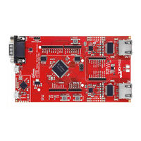
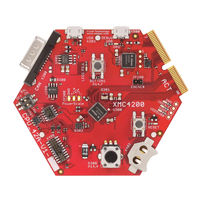
Infineon XMC4000 series Board User's Manual (35 pages)
Hexagon Application Kit, CPU Board
Brand:
Infineon
| Category:
Microcontrollers
| Size: 1.72 MB
Table of Contents
Table of Contents
4
Introduction
7
Key Features
7
Block Diagram
8
Figure 1 CPU_45B-V1 Board Block Diagram
8
Figure 2 CPU Board XMC4500 SDRAM (CPU_45B-V1)
9
1 Overview
7
2 Hardware Description
9
Power Supply
9
Figure 3 Powering Option
10
Figure 4 Block Diagram of Power Supply
10
Table 1 Power Status Leds
10
Table 2 Power Measurement
11
Figure 5 Reset Circuit
12
Figure 6 Reset LED and Reset Button
12
Reset
12
Boot Option
13
Clock Generation
13
Figure 7 Clock Generation Circuit
13
Figure 8 Boot Options Switch
13
Table 3 Boot Options Settings
13
Debug Interface
14
Figure 10 On-Board USB Debugger
15
Figure 9 Installation of Serial Port Driver
15
On-Board USB Debugger
15
Cortex Debug Connector (10-Pin)
16
Figure 11 Cortex Debug Connector (10-Pin)
16
Table 4 Cortex Debug Connector (10 Pin)
16
Cortex Debug+Etm Connector (20-Pin)
17
Figure 12 Cortex Debug Connector (10-Pin) Layout
17
Figure 13 Cortex Debug+Etm Connector (20-Pin)
17
Figure 14 Cortex Debug+Etm Connector (20-Pin) Layout
18
Table 5 Cortex Debug+Etm Connector (20 Pin)
18
Figure 15 Quad SPI Flash Interface
19
Serial Flash Memory
19
Table 6 Quad SPI Signals
19
Figure 16 SDRAM Interface
20
Figure 17 USB Connector
20
Sdram
20
Usb
20
Figure 18 USB Power Generation - Host/Otg Mode
21
Table 7 USB Micro AB Connector Pinout
21
Figure 19 Battery Holder for Coin Cells
22
Figure 20 XMC4500 Power Domains and Real Time Clock
22
Rtc
22
Figure 21 User Leds and User Buttons
23
Potentiometer
23
Table 10 Potentiometer
23
Table 8 User Leds
23
Table 9 User Buttons
23
User Leds and User Button
23
Figure 22 Satellite Connectors
24
Satellite Connectors
24
COM Connector
25
Figure 23 Satellite Connector Type COM
25
Figure 24 Satellite Connector Type HMI
26
HMI Connector
26
ACT Satellite Connector
27
Figure 25 Satellite Connector Type ACT
27
Infineon XMC4000 series Device Manual (38 pages)
For Industrial Applications
Brand:
Infineon
| Category:
Microcontrollers
| Size: 1.27 MB
Table of Contents
Table of Contents
4
1 Hibernate Mode Basics
6
Externally Controlled Hibernate Use Cases
7
Internally Controlled Hibernate Use Cases
8
2 Hibernate Mode Implementations
11
Externally Controlled Hibernate Mode Concept
11
Internally Controlled Hibernate Mode Concept
13
3 Control of External Voltage Regulator
16
Active High Enable Via Pull-Up
17
Active High Enable Driven from a Voltage Divider
18
Active Low Enable Driven with Push-Pull I/O
19
Active Low Enable and with Pull-Up to High
20
Active Low Enable Driven from a Voltage Divider
20
Active Low Enable Driven from a Voltage Divider and
21
Bat
21
4 Getting Started
24
Initialize Hibernate Domain
25
Store Context Data in Retention Memory
26
Select Wake-Up Triggers
27
Configure Hibernate Control I/O
28
Request External Hibernate Mode
29
Request Internal Hibernate Mode
29
Hibernate Mode Entered
30
Wake-Up Trigger Detected
30
Power-Up and Boot-Up
31
Processing of Wake-Up Cause Info
31
Clear Reset Status
32
Restore Context Data from Retention Memory
32
Execute Application Code
32
5 Application Hints
35
Which Hibernate Mode to Choose
35
Hibernate Domain Clock
35
Digital I/O Voltage Levels
36
Analog I/O Voltage Levels
36
Retention Memory
36
Emergency Recovery from Hibernate Mode
37
Infineon XMC4000 series User Manual (30 pages)
Brand:
Infineon
| Category:
Motherboard
| Size: 4.91 MB
Table of Contents
Table of Contents
4
Introduction
6
Table 1 Kit Specification
6
Key Features
7
Table 2 Kit Features of Assembly Versions
7
Block Diagram
8
Hardware Description
8
Figure 1 Block Diagram of the XMC4400 Platform2Go Series-V1
8
Figure 2 XMC4400 Platform2Go 3.3V
9
Figure 3 XMC4400 Platform2Go 5V
9
Figure 4 XMC4400 Platform2Go 3.3V Lite
10
Figure 5 XMC4400 Platform2Go 5V Lite
10
Power Supply
11
Figure 6 Power Supply Concept
11
Figure 7 Signal Mapping of the Pin Headers X1 and X2
12
Pin Header for Microbus and Shield2Go Connector 1 and 2
13
Figure 8 Signal Mapping of the Pin Headers for Microbus and Shield2Go Connector 1 and 2
13
Solderable 0 Ohm Pin Bridges
14
Table 3 Signal Mapping of the 0 Ohm Pin Bridges
14
Arduino Compatible Connector
15
Figure 9 Mapping of Arduino Functions to XMC Pin Functions
15
User Push Buttons and User Leds
16
On-Board Debug Probe
16
UART Communication for XMC4200
16
Table 4 XMC4400 Pin Mapping for User Leds
16
Table 5 XMC4400 Pin Mapping for User Push Buttons and Potentiometer
16
Table 6 XMC4400 Pins Mapping for Debugging and UART-Communication
16
Cortex™ Debug Connector (10-Pin)
17
Reset
17
CAN Transceiver
17
Table 7 Pin Assignment of the Cortex™ Debug Connector (X102)
17
Table 8 CAN Signals and XMC4400 Pin Mapping
17
Serial Flash Memory
18
Ethernet
18
Table 9 XMC4400 Pins Mapping for Serial Flash Memory
18
Table 10 XMC4400 Pins Used for Ethernet
18
Boot Option
19
Production Data
19
Schematics
19
Table 11 Boot Mode Selection with External Pull Resistors
19
Figure 10 Connectors Schematic: Pin Header, Pin Bridges, Level Shifter, Microbus, Shield2Go
20
Figure 11 Xmc_4400_Debug Schematic: OBD Probe, Ethernet, Quad-SPI Memory
21
List of Material
25
Table 12 List of Material
25
Infineon XMC4000 series Board User's Manual (28 pages)
Brand:
Infineon
| Category:
Motherboard
| Size: 5.07 MB
Table of Contents
Table of Contents
4
1 Introduction
6
Table 1 Kit Specification
6
Key Features
7
Table 2 Kit Features of Assembly Versions
7
Block Diagram
8
2 Hardware Description
8
Figure 1 Block Diagram of the XMC4200 Platform2Go Series-V1.1
8
Figure 2 XMC4200 Platform2Go 3.3V
9
Figure 3 XMC4200 Platform2Go 5V
9
Figure 4 XMC4200 Platform2Go 3.3V Lite
10
Figure 5 XMC4200 Platform2Go 5V Lite
10
Power Supply
11
Figure 6 Power Supply Concept
11
Pin Header X1 and X2
12
Figure 7 Signal Mapping of the Pin Headers X1 and X2
12
Pin Header for Microbus and Shield2Go Connector 1 and 2
13
Figure 8 Signal Mapping of the Pin Headers for Microbus and Shield2Go Connector 1 and 2
13
Solderable 0 Ohm Pin Bridges
14
Table 3 Signal Mapping of the 0 Ohm Pin Bridges
14
Arduino Compatible Connector
15
Figure 9 Mapping of Arduino Functions to XMC Pin Functions
15
User Push Buttons, Potentiometer and User Leds
16
On-Board Debug Probe
16
UART Communication for XMC4200
16
Cortex™ Debug Connector (10-Pin)
16
Table 4 XMC4200 Pin Mapping for User Leds
16
Table 5 XMC4200 Pin Mapping for User Push Buttons and Potentiometer
16
Table 6 XMC4200 Pins Mapping for Debugging and UART-Communication
16
Reset
17
CAN Transceiver
17
Table 7 Pin Assignment of the Cortex™ Debug Connector (X102)
17
Table 8 CAN Signals and XMC4200 Pin Mapping
17
Boot Option
18
3 Production Data
18
Schematics
18
Table 9 Boot Mode Selection with External Pull Resistors
18
Figure 10 Connectors Schematic: Pin Header, Pin Bridges, Level Shifter, Microbus, Shield2Go
19
Figure 11 Xmc_4200_Debug Schematic: OBD Probe
20
Figure 12 XMC4200 Schematic: USB Connector, Microcontroller Pins and Power, Potentiometer Button and
21
List of Material
24
Table 10 List of Material
24
Infineon XMC4000 series User Manual (17 pages)
POSIF in Triple-Hall Mode, Triple-Hall Commutation Control for BLDC Motors
Brand:
Infineon
| Category:
Microcontrollers
| Size: 2.37 MB
Table of Contents
Table of Contents
4
1 Triple-Hall Commutation Control for BLDC Motors
6
Figure 1 BLDC Motor Control with Triple-Hall Commutation
6
2 Triple-Hall Input Pattern
7
Delayed Hall Input Sampling
7
Figure 2 the Triple-Hall Input Samples Stage for a BLDC Motor Commutation Control
7
Figure 3 Triple-Hall Input Samples Edge Detection
7
Shadow Update of Expected Patterns
8
Verification of Hall Event Input Patterns
8
Hall Event Verification Outputs
8
Figure 4 Triple-Hall Input Samples Verification and Administration of Expected Samples
8
Administration (Shadow Transfer) of Pattern Compare Values
9
Output Pattern Control
9
3 Triple-Hall Output Pattern for BLDC Motor Commutation Control
9
Output Pattern Control by CAPCOM Slices in Multi-Channel Mode
9
Output Pattern Control by CAPCOM Slices in External Modulation Mode
10
Figure 5 Triple-Hall BLDC Motor Commutation Control Using CAPCOM Units in Multi-Channel Mode
10
Figure 6 Triple-Hall BLDC Motor Commutation Control by Capcom:s in External Modulation Mode
11
4 POSIF Interrupt Registers
12
POSIF Interrupts/Event Requests in Hall Sensor Mode
12
POSIF Interrupts/Event Requests in Multi-Channel Mode
12
5 Getting Started with POSIF in Triple-Hall Mode
13
POSIF Global Registers
13
POSIF Setup When Using Hall Sensor Mode
13
POSIF Setup When Using Multi-Channel Features in Hall Sensor Mode
13
POSIF Input Selections in Hall Sensor Mode
13
POSIF Operation Mode Associated Registers
13
POSIF Associated Configurations of Ccu4X/-8X Timers
13
POSIF Synchronized Start of Timers by HW Initialization
13
POSIF Optional Setup Selections in Hall Mode
13
Timer Setup
14
Ultimate Initialization Sequence
14
Ultimate Start-Up Enable
14
Setting the Timer Counting Modes
14
Setting Compare Mode Control
14
Setting the Output Pins PASSIVE / ACTIVE Level Control
14
External Events Control Setup Registers
14
Multi-Channel Mode Enable
14
Multi-Channel Synchronization to Shadow Transfers
15
Using the POSIF Global Registers for Hall Sensor Mode Setup
15
Using the POSIF Global and Multi-Channel (MC) Mode Setup Registers
15
Using the Timer Control Registers for COMPARE Mode
15
Using the Timer Control Registers for MULTI-CHANNEL Mode
16
Using the Timer Control Registers for EXTERNAL MODULATION Mode
16
Using the Register Bitfields for EXTERNAL EVENTS CONTROL
16
Using the External Events Control Registers for START
16
Infineon XMC4000 series User Manual (14 pages)
CCU8 and Output State Override, Output State Override on External Events
Brand:
Infineon
| Category:
Microcontrollers
| Size: 0.76 MB
Table of Contents
Table of Contents
4
1 Output State Override on External Events
6
Use Cases
6
2 External Events Control of a Timer Output State
8
External Events Control of Timer Input Functions in General
8
Selection of External Events Control Sources and Input Functions
8
Figure 1 Use Case - Current Control and Protection by Monitoring Using Output State Override
8
Figure 2 External Events Control of a Timer Slice Input Functions
8
Output Pin PASSIVE / ACTIVE Level Control
9
3 Output State Override
10
Figure 3 Output State Override Illustration
10
4 Getting Started with CCU8 and Output State Override
11
Ultimate Initialization Sequence
11
Ultimate Start-Up Enable
11
External Events Control Setup Registers
11
Using the Output State Override Control Register Bitfields
11
Pseudo Code for the Output State Override Setup
11
Figure 5 Setting Output State Override Parameters (Control Registers)
12
5 Example Application for CCU8 and Output State Override
13
Principle of Peak&Hold with Current Limitation by Output State Override
13
Figure 6 Principle of Peak&Hold with Current Limitation by Output State Override
13
Infineon XMC4000 series User Manual (14 pages)
CCU8 and Cross Interconnections Top-Level Interconnect Control
Brand:
Infineon
| Category:
Microcontrollers
| Size: 0.96 MB
Table of Contents
Table of Contents
4
1 Top Level Interconnect Control
6
Figure 1 the Top-Level (Cross) Interconnect Matrix
6
2 Top-Level Control of Event Requests To/From a Timer Slice
7
Figure 2 Example with an ADC Cross Connected to a Timer Via the Top-Level Interconnect Matrix
7
CCU8 Using Top-Level Interconnect Control with Event Request Unit (ERU)
8
CCU8 and ERU Use Cases
8
Figure 3 Top-Level Interconnect with Conditional Event Request Control by the Event Request Unit
8
Example - Using CCU8 and ERU1 for Delayed ADC-Start Controlled by an IO
10
Figure 4 Details of a CCU8 Timer Slice System Interactions by Top-Level Interconnect Control
10
Figure 5 Using CCU8 and ERU1 for Delayed ADC Start Controlled by an IO
10
3 Getting Started with CCU8 and Cross Interconnections
11
Getting Started with the CAPCOM8 Unit Ccu8X
11
Using the CAPCOM8 External Events Control Setup Registers
11
CAPCOM8 External Event Control Register Bitfields
11
Getting Started with Event Request Unit - ERU1
11
Cross Interconnection Example - Using CCU8, ERU1, ADC and GPIO
11
ADC Request on Port Pin P1.15 State and the Timer CCU80CC81 Status Bit
11
Event Request Unit Block Diagrams and Control Registers
13
Figure 6 Event Request Unit Block Diagrams and Control Registers
13
Infineon XMC4000 series User Manual (11 pages)
CCU8 and Capture Mode Features
Brand:
Infineon
| Category:
Microcontrollers
| Size: 0.57 MB
Table of Contents
Table of Contents
4
1 Advanced Signal Measurement
6
Slice Timer Setup in Capture Mode
6
The Capture Algorithm
7
Disabling the Full-Flags
7
Capture by External Events Control
7
Timer Inputs for Capture
8
External Control by Capture Events
8
Top-Level Control of Event Requests To/From a Timer in Capture Mode
8
2 Getting Started with CCU8 and Capture Mode Features
9
Ultimate Initialization Sequence
9
Ultimate Start-Up Enable
9
External Events Control Setup Registers
9
Using the External Capture Control Register Bitfields
9
Pseudo Code for the Capture0 or Capture1 Setup
9
Infineon XMC4000 series Application Manual (10 pages)
For Industrial Applications
Brand:
Infineon
| Category:
Microcontrollers
| Size: 0.31 MB
Advertisement
Related Products
Infineon XMC4500 series
Infineon XMC4200
Infineon XMC4400
Infineon XMC4500 SDRAM
Infineon DriveCard XMC4400 V1
Infineon XMC4700
Infineon XMC Series
Infineon XMC1000
Infineon XMC1400
Infineon XMC1100
Infineon Categories
Motherboard
Microcontrollers
Computer Hardware
Control Unit
Controller
More Infineon Manuals
Login
Sign In
OR
Sign in with Facebook
Sign in with Google
Upload manual
Upload from disk
Upload from URL