Table of Contents
Advertisement
Quick Links
QQ
3 7 63 1515 0
SERVICE MANUAL
Ver 1.0 2001.06
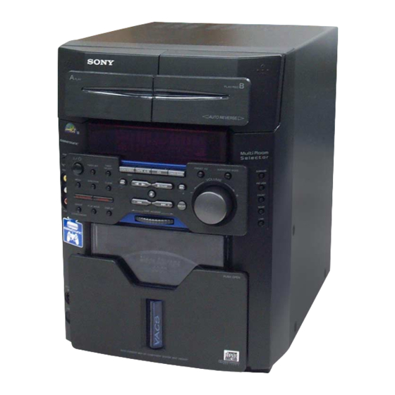
HCD-VM330AV is the Amplifier, Video CD/CD player,
Tape Deck and Tuner section in MHC-VM330AV.
This stereo system is equipped with the Dolby* Pro
Logic Surround decoder.
* Manufactured under license from Dolby
Laboratories. Dolby , Pro Logic , and the
double-D symbol ; are trademarks of Dolby
Laboratories. Confidential unpublished works.
'1992-1997 Dolby Laboratories. All rights
reserved.
TE
L 13942296513
Amplifier section
Front speaker:
Continuous RMS power output
Total harmonic distortion less than 0.09%
Center speaker:
Continuous RMS power output
Rear speaker:
Continuous RMS power output
Inputs
VIDEO/MD IN (phono jacks):
5.1CH:
FRONT (phono jacks)
REAR (phono jacks)
CENTER (phono jack)
SUB WOOFER (phono jack):
www
.
Sony Corporation
9-873-189-01
2001F0500-1
Home Audio Company
C 2001.6
Shinagawa Tec Service Manual Production Group
http://www.xiaoyu163.com
Outputs
PHONES (stereo phone jack):
75 + 75 watts
FRONT SPEAKER:
(8 ohms at 1 kHz,
10% THD)
SURROUND SPEAKER REAR:
(8 ohms at 1 kHz,
40 watts)
SURROUND SPEAKER CENTER:
25 watts
SUB WOOFER:
(8 ohms at 1 kHz,
10% THD)
VIDEO OUT (phono jack):
25 + 25 watts
(8 ohms at 1 kHz,
10% THD)
S-VIDEO OUT (4-pin/mini-DIN jack)
voltage 250 mV/450 mV,
impedance 47 kilohms
voltage 450 mV,
impedance 47 kilohms
voltage 450 mV,
impedance 47 kilohms
voltage 450 mV,
impedance 47 kilohms
voltage 450 mV,
impedance 47 kilohms
x
ao
y
i
http://www.xiaoyu163.com
HCD-VM330AV
8
Model Name Using Similar Mechanism
CD Mechanism Type
CD
Section
Base Unit Name
Optical Pick-up Name
Model Name Using Similar Mechanism
TAPE
Q Q
Section
Tape Transport Mechanism Type
3
6 7
1 3
SPECIFICATIONS
accepts headphones of
8 ohms or more
accepts impedance of 8 to
16 ohms
accepts impedance of 8 to
16 ohms
accepts impedance of
8 ohms
voltage 1 V,
impedance 1 kilohm
max. output level 1 Vp-p,
unbalanced,
Sync negative,
load impedance 75 ohms
Y: 1 Vp-p, unbalanced,
Sync negative,
C: 0.286 Vp-p, load
impedance 75 ohms
COMPACT DISC DECK RECEIVER
u163
.
2 9
9 4
2 8
NEW
CDM64-30ABD61A
BU-30ABD61A
OP Assy (A-MAX. 3)
HCD-MG110
CM8L6Z511A
1 5
0 5
8
2 9
9 4
VIDEO CD/CD player section
System
Laser
Frequency response
Wavelength
Signal-to-noise ratio
Dynamic range
Video color system format NTSC, PAL
OPTICAL OUT (CD)
(Square optical connector jack, rear panel)
Wavelength
Output Level
Tape player section
Recording system
Frequency response
– Continued on next page –
m
co
9 9
E Model
2 8
9 9
Compact disc and digital
audio system
Semiconductor laser
(λ = 795 nm)
Emission duration:
continuous
2 Hz – 20 kHz (±0.5 dB)
775 – 815 nm
More than 90 dB
More than 90 dB
660 nm
–18 dBm
4-track 2-channel stereo
40 – 13,000 Hz (±3 dB),
using Sony TYPE I
cassette
Advertisement
Table of Contents

Related Manuals for Sony HCD-VM330AV


Summary of Contents for Sony HCD-VM330AV
-
Page 1: Service Manual
3 7 63 1515 0 SERVICE MANUAL E Model Ver 1.0 2001.06 HCD-VM330AV is the Amplifier, Video CD/CD player, Tape Deck and Tuner section in MHC-VM330AV. This stereo system is equipped with the Dolby* Pro Model Name Using Similar Mechanism Logic Surround decoder. -
Page 2: Table Of Contents
HCD-VM330AV 3 7 63 1515 0 Tuner section General FM stereo, FM/AM superheterodyne tuner Power requirements 110 – 120 V or 220 – 240 V AC, 50/60 Hz FM tuner section Adjustable with voltage selector Tuning range 87.5 – 108.0 MHz... - Page 3 LINE WITH MARK 0 ON THE SCHEMATIC DIAGRAMS AND IN THE PARTS LIST ARE CRITICAL TO SAFE OPERATION. REPLACE THESE COMPONENTS WITH SONY PARTS WHOSE PART NUMBERS APPEAR AS SHOWN IN THIS MANUAL OR IN SUPPLEMENTS PUB- LISHED BY SONY.
-
Page 4: Servicing Note
HCD-VM330AV SECTION 1 SERVICING NOTES 3 7 63 1515 0 CD-TEXT TEST DISC CLEANING OBJECTIVE LENS OF OPTICAL PICK-UP • In cleaning the objective lens of optical pick-up, be sure the following below. This unit is able to display the test data (character information) written in the CD on its fluorescent indicator tube. -
Page 5: General
HCD-VM330AV SECTION 2 This section is extracted from instruction manual. 3 7 63 1515 0 GENERAL Parts Identification The items are arranged in alphabetical order. Refer to the pages indicated in parentheses ( ) for details. Main unit 2 3 4 56 7 8 w;... -
Page 6: Setting The Time
HCD-VM330AV 3 7 63 1515 0 Setting the time Remote Control Turn on the system. 1 2 3 4 Press TIMER SET (or CLOCK/TIMER SET on the remote). When you set the clock for the first time, go to step 5. -
Page 7: Disassembly
HCD-VM330AV SECTION 3 DISASSEMBLY 3 7 63 1515 0 • This set can be disassembled in the order shown below. 3-1. DISASSEMBLY FLOW Note 1: The process described in can be performed in any order. Note 2: Without completing the process described in , the next process can not be performed. -
Page 8: Upper Cover
HCD-VM330AV 3 7 63 1515 0 Note: Follow the disassembly procedure in the numerical order given. 3-2. UPPER COVER 2 five screws 3 upper cover (BVTP3 × 8) 2 two screws (BVTP3 × 8) 1 three screws (BVTP3 × 8) 1 three screws (BVTP3 ×... -
Page 9: Video Board
HCD-VM330AV 3 7 63 1515 0 3-4. VIDEO BOARD 1 wire (flat type) (25 core) 6 VIDEO board (CN501) 3 two screws (BVTP3 × 10) 2 screw (BVTP3 × 8) 4 MPEG bracket 1 wire (flat type) (13 core) -
Page 10: Back Panel, Dc Fan (M391)
HCD-VM330AV 3 7 63 1515 0 3-6. BACK PANEL, DC FAN (M391) 3 four screws (BVTP3 × 10) 1 two screws (BVTP3 × 10) 5 back panel 1 two screws (BVTP3 × 10) 4 DC fan (M391) 1 thirteen screws (BVTP3 ×... -
Page 11: Middle (F) Assy, Bracket (Middle-R), Power Bracket
HCD-VM330AV 3 7 63 1515 0 3-8. MIDDLE (F) ASSY, BRACKET (MIDDLE-R), POWER BRACKET 7 bracket (middle-R) 6 two screws (BVTP3 × 8) 5 three screws (BVTP3 × 8) 3 screw (BVTP3 × 8) 2 two screws (BVTP3 × 8) 9 three screws (BVTP3 ×... -
Page 12: Base Unit (Bu-30Abd61A)
HCD-VM330AV 3 7 63 1515 0 3-10. BASE UNIT (BU-30ABD61A) 3 base unit (BU-30ABD61A) 2 bracket (top 60) 1 three screws (BVTP3 × 8) L 13942296513 3-11. BU HOLDER ASSY 1 tension spring (F1) 2 tension spring (F-2) 3 two screws (PTP2.6 ×... -
Page 13: Cassette Lid Assy (A)/(B)
HCD-VM330AV 3 7 63 1515 0 3-12. CASSETTE LID ASSY (A) / (B) 1 Open the cassette lid assy (A)/(B). 2 two claws 3 cassette lid assy (A) 5 cassette lid assy (B) 4 two claws L 13942296513 3-13. MECH DECK (TAPE) 1 three screws (BVTP3 ×... -
Page 14: Test Mode
HCD-VM330AV SECTION 4 3 7 63 1515 0 TEST MODE [MC Cold Reset] [CD Service Mode] • The cold reset clears all data including preset data stored in the • This mode can run the CD sled motor optionally. Use this mode, RAM to initial conditions. -
Page 15: Mechanical Adjustments
HCD-VM330AV SECTION 5 SECTION 6 MECHANICAL ADJUSTMENTS ELECTRICAL ADJUSTMENTS 3 7 63 1515 0 • TAPE MECHANISM DECK SECTION DECK SECTION 0 dB = 0.775 V Precaution 1. Clean the following parts with a denatured alcohol-moistened Precaution swab: 1. Demagnetize the record/playback head with a head demagne-... - Page 16 HCD-VM330AV 3 7 63 1515 0 Record/Playback Head Azimuth Adjustment Adjustment Location: Playback Head (Deck A). Record/Playback/Erase Head (Deck B). DECK A DECK B Note: Perform this adjustments for both decks forward Procedure: 1. Mode: Playback (FWD) test tape...
-
Page 17: Cd Section
HCD-VM330AV 3 7 63 1515 0 Note: Clear RF signal waveform means that the shape “◊” can be CD SECTION clearly distinguished at the center of the waveform. Note : RF signal waveform 1. CD Block is basically designed to operate without adjustment. -
Page 18: Video Section
HCD-VM330AV 3 7 63 1515 0 Checking Location : VIDEO SECTION Video Frequency Adjustment [ BD BOARD ] — SIDE B — Connection: frequency counter VMP board TP (27MHz) TP (GND) R120 Procedure: TP (DVC) 1. Connect a frequency counter to TP (27MHz) and TP (GND). -
Page 19: Sensor Section
HCD-VM330AV 3 7 63 1515 0 SENSOR SECTION Disc Sensor Level Adjustment Procedure: Connect an oscilloscope to TP (DISC SENSOR) and TP (GND) on the MAIN board. Turn the power on. In the no disc status, adjust RV301 on the MAIN board so that the waveform of oscilloscope becomes as below. - Page 20 HCD-VM330AV 3 7 63 1515 0 MEMO L 13942296513 u163 http://www.xiaoyu163.com...
-
Page 21: Diagrams
HCD-VM330AV SECTION 7 3 7 6 3 1 5 1 5 0 DIAGRAMS 7-1. BLOCK DIAGRAM – CD SERVO Section – FILTER XTSL DIGITAL SIGNAL PROCESSOR RF AMP, IC101 (1/2) FOCUS/TRACKING ERROR AMP 53 55 52 54 XTAO IC103... -
Page 22: Block Diagram - Audio/Video Section
HCD-VM330AV 3 7 6 3 1 5 1 5 0 7-2. BLOCK DIAGRAM – AUDIO/VIDEO Section – DIGITAL FILTER, D/A CONVERTER IC509 MCLK 33.8MHz (Page 21) MPEG VIDEO/AUDIO DECODER, DIGITAL DATA DA-DATA VOUTL CD L-CH VIDEO SIGNAL PROCESSOR MPEG... -
Page 23: Block Diagram - Tuner/Tape Deck Section
HCD-VM330AV 3 7 6 3 1 5 1 5 0 7-3. BLOCK DIAGRAM – TUNER/TAPE DECK Section – TUNER PACK TUNER L-CH FM ANT L-CH (Page 24) FM 75Ω ANT GND R-CH R-CH ANTENNA AM ANT ANT GND TU-CLK... -
Page 24: Block Diagram - Surround Section
HCD-VM330AV 3 7 6 3 1 5 1 5 0 7-4. BLOCK DIAGRAM – SURROUND Section – LOW-PASS FILTER IC304 (1/2) SPE ANA (Page 26) R-CH DOLBY PRO LOGIC SURROUND PROCESSOR R-CH IC301 L-CH SWVOL (Page 23) WOOFER SWIN... -
Page 25: Block Diagram - Amp Section
HCD-VM330AV 3 7 6 3 1 5 1 5 0 7-5. BLOCK DIAGRAM – AMP Section – J503 PHONE J501 (1/2) FRONT L-CH DBFB AMP (Page 24) IC303 POWER AMP – IC501 FRONT SPEAKER R-CH – RY501 MUTING MUTING... -
Page 26: Block Diagram - Display/Power Supply Section
HCD-VM330AV 3 7 6 3 1 5 1 5 0 7-6. BLOCK DIAGRAM – DISPLAY/POWER SUPPLY Section – GRID DRIVE LED DRIVE D703 – 707 Q721 – 723 Q713 – 717 LED DRIVE D708, 736, FL701 Q702 – 705, 718... -
Page 27: Note For Printed Wiring Boards And Schematic Diagrams
HCD-VM330AV 3 7 6 3 1 5 1 5 0 7-7. NOTE FOR PRINTED WIRING BOARDS AND SCHEMATIC DIAGRAMS • Circuit Boards Location (In addition to this, the necessary note is printed in each block) VIDEO board Note on Schematic Diagram: Note on Printed Wiring Boards: •... -
Page 28: Printed Wiring Board - Bd Section
HCD-VM330AV 3 7 6 3 1 5 1 5 0 7-8. PRINTED WIRING BOARD – BD Section – • See page 27 for Circuit Boards Location. IC102 TP (DVC) TP (FEI) TP (FEO) IC104 TP (TEO) 1 3 9 4 2 2 9 6 5 1 3... -
Page 29: Schematic Diagram - Bd Section
HCD-VM330AV 3 7 6 3 1 5 1 5 0 7-9. SCHEMATIC DIAGRAM – BD Section – • • See page 43 for Waveforms. See page 52 for IC Block Diagrams. TP (RFAC) (FEI) IC 106 TP (RFDC) Q101... -
Page 30: Printed Wiring Board - Audio/Video Section
HCD-VM330AV 3 7 6 3 1 5 1 5 0 7-10. PRINTED WIRING BOARDS – AUDIO/VIDEO Section – • See page 27 for Circuit Boards Location. MAIN BOARD (Page 42) VIDEO BOARD VIDEO BOARD (SIDE A) (SIDE B) CN316... -
Page 31: Schematic Diagram - Audio/Video Section (1/3)
HCD-VM330AV 3 7 6 3 1 5 1 5 0 7-11. SCHEMATIC DIAGRAM – AUDIO/VIDEO Section (1/3) – • See page 43 for Waveform. VIDEO LEVEL SHIFT CL680 RESET VIDEO CD CONTROLLER IC502 M30622MGA-A58FP 1 3 9 4 2 2 9 6 5 1 3... -
Page 32: Schematic Diagram - Audio/Video Section (2/3)
HCD-VM330AV 7-12. SCHEMATIC DIAGRAM – AUDIO/VIDEO Section (2/3) – • See page 43 for Waveforms. 3 7 6 3 1 5 1 5 0 (Page 31) VIDEO BOARD (1/3) VIDEO Q502 VIDEO BOARD DTC114EKA- (3/3) T146 BUFFER (Page 33) -
Page 33: Schematic Diagram - Audio/Video Section (3/3)
HCD-VM330AV 7-13. SCHEMATIC DIAGRAM – AUDIO/VIDEO Section (3/3) – • • See page 43 for Waveforms. See page 52 for IC Block Diagrams. 3 7 6 3 1 5 1 5 0 J301 VIDEO S-VIDEO OUT CN301 MAIN BOARD (2/4) -
Page 34: Printed Wiring Boards - Cd Motor/Sensor Section
HCD-VM330AV 3 7 6 3 1 5 1 5 0 7-14. PRINTED WIRING BOARDS – CD MOTOR/SENSOR Section – • See page 27 for Circuit Boards Location. (Page 42) MAIN BOARD CN305 T SENSOR BOARD L. T MOTOR BOARD... -
Page 35: Schematic Diagram - Cd Motor/Sensor Section
HCD-VM330AV 3 7 6 3 1 5 1 5 0 7-15. SCHEMATIC DIAGRAM – CD MOTOR/SENSOR Section – (Page 40) (Page 40) 1 3 9 4 2 2 9 6 5 1 3 (Page 40) (Page 40) (Page 40) •... -
Page 36: Printed Wiring Board - Tc Section
HCD-VM330AV 3 7 6 3 1 5 1 5 0 7-16. PRINTED WIRING BOARD – TC Section – • See page 27 for Circuit Boards Location. MAIN BOARD (Page 42) CN311 TC BOARD 1 3 9 4 2 2 9 6 5 1 3... -
Page 37: Schematic Diagram - Tc Section
HCD-VM330AV 3 7 6 3 1 5 1 5 0 7-17. SCHEMATIC DIAGRAM – TC Section – • See page 52 for IC Block Diagram. (Page 38) 1 3 9 4 2 2 9 6 5 1 3 w w w u 1 6 3 •... -
Page 38: Schematic Diagram - Main Section (1/4)
HCD-VM330AV 3 7 6 3 1 5 1 5 0 7-18. SCHEMATIC DIAGRAM – MAIN Section (1/4) – (Page 45) 1 3 9 4 2 2 9 6 5 1 3 (Page (Page 37) w w w u 1 6 3 (Page 40) •... -
Page 39: Schematic Diagram - Main Section (2/4)
HCD-VM330AV 3 7 6 3 1 5 1 5 0 7-19. SCHEMATIC DIAGRAM – MAIN Section (2/4) – (Page 47) 1 3 9 4 2 2 9 6 5 1 3 (Page 38) (Page 33) (Page 51) (Page 45) -
Page 40: Schematic Diagram - Main Section (3/4)
HCD-VM330AV 3 7 6 3 1 5 1 5 0 7-20. SCHEMATIC DIAGRAM – MAIN Section (3/4) – • See page 52 for IC Block Diagram. (Page 38) (Page 39) (Page 47) 1 3 9 4 2 2 9 6 5 1 3... -
Page 41: Schematic Diagram - Main Section (4/4)
HCD-VM330AV 3 7 6 3 1 5 1 5 0 7-21. SCHEMATIC DIAGRAM – MAIN Section (4/4) – • See page 43 for Waveforms. (Page 39) 1 3 9 4 2 2 9 6 5 1 3 IC801 M30622MGA-A57FP... -
Page 42: Printed Wiring Board - Main Section
HCD-VM330AV 3 7 6 3 1 5 1 5 0 7-22. PRINTED WIRING BOARD – MAIN Section – • See page 27 for Circuit Boards Location. (Page 46) (Page 36) (Page 46) (Page 30) TAPE GAME LINK MECHANISM DECK... - Page 43 HCD-VM330AV 3 7 6 3 1 5 1 5 0 • Semiconductor • Waveforms Location – BD Board – – VIDEO Board – – MAIN Board – Ref. No. Location 1 IC101 t; (RFAC) (CD Play mode) 1 IC502 qd (XOUT) 6 IC505 <z/,>...
-
Page 44: Printed Wiring Boards - Amp Section
HCD-VM330AV 3 7 6 3 1 5 1 5 0 7-23. PRINTED WIRING BOARDS – AMP Section – • See page 27 for Circuit Boards Location. • Semiconductor Location Ref. No. Location D501 D502 D503 H-11 D504 D507 D508... -
Page 45: Schematic Diagram - Amp Section
HCD-VM330AV 3 7 6 3 1 5 1 5 0 7-24. SCHEMATIC DIAGRAM – AMP Section – (Page 41) (Page 38) 1 3 9 4 2 2 9 6 5 1 3 (Page 51) (Page 39) w w w u 1 6 3 •... -
Page 46: Printed Wiring Boards - Display Section
HCD-VM330AV 3 7 6 3 1 5 1 5 0 7-25. PRINTED WIRING BOARDS – DISPLAY Section – • See page 27 for Circuit Boards Location. DISPLAY BOARD FL701 FLUORESCENT INDICATOR TUBE CNP707 X701 D707, S745 SURROUND CNP308 D706, S744... -
Page 47: Schematic Diagram - Display Section
HCD-VM330AV 3 7 6 3 1 5 1 5 0 7-26. SCHEMATIC DIAGRAM – DISPLAY Section – • • See page 43 for Waveform. See page 52 for IC Block Diagram. 1 3 9 4 2 2 9 6 5 1 3... -
Page 48: Printed Wiring Board - Control Section
HCD-VM330AV 3 7 6 3 1 5 1 5 0 7-27. PRINTED WIRING BOARD – CONTROL Section – • See page 27 for Circuit Boards Location. CONTROL BOARD TUNER/BAND TAPE A/B 5.1CH/VIDEO (MD) D736, S700 TIMER I / 1... -
Page 49: Schematic Diagram - Control Section
HCD-VM330AV 3 7 6 3 1 5 1 5 0 7-28. SCHEMATIC DIAGRAM – CONTROL Section – (Page 47) 1 3 9 4 2 2 9 6 5 1 3 • Voltages and waveforms are dc with respect to ground under no-signal (detuned) conditions. -
Page 50: Printed Wiring Boards - Power Section
HCD-VM330AV 3 7 6 3 1 5 1 5 0 7-29. PRINTED WIRING BOARDS – POWER Section – • See page 27 for Circuit Boards Location. POWER BOARD VOL SEL BOARD F903 (AC IN) S901 VOLTAGE SELECTOR 110 – 120V t 220 – 240V... -
Page 51: Schematic Diagram - Power Section
HCD-VM330AV 3 7 6 3 1 5 1 5 0 7-30. SCHEMATIC DIAGRAM – POWER Section – (Page 45) 1 3 9 4 2 2 9 6 5 1 3 (Page 39) w w w • Voltages and waveforms are dc with respect to ground... - Page 52 HCD-VM330AV 3 7 6 3 1 5 1 5 0 • IC Block Diagrams IC103 CXA2581N-T4 – BD Board – RW/ROM IC101 CXD3068Q DC OFST RFDCI – – RFDCO 59 58 57 56 55 54 53 52 51 50 49 48...
- Page 53 HCD-VM330AV 3 7 63 1515 0 – VIDEO Board – IC302 NJM2255M (TE2) IC303 NJM2209M (TE2) SATURATION +Ø ADJUST (COLOR BURST) HUE ADJUST SECONDARY LOWER CLAMP SATURATION DIFFERENTIATION LIMITER SYNC ADJUST GAIN ADJ CHIP –X (COLOR BURST) SWITCH CONTROL...
- Page 54 HCD-VM330AV 3 7 63 1515 0 – TC Board – IC401 TA8189N METAL TAPE A CH2/A CH2/B /TAPE B – – VREF1 IREF VREF2 – – CH1/A CH1/B METAL GND1 – MAIN Board – – DISPLAY Board – IC881 BA6780...
-
Page 55: Ic Pin Function Description
HCD-VM330AV 3 7 63 1515 0 7-31. IC PIN FUNCTION DESCRIPTION • BD BOARD IC101 CXD3068Q (DIGITAL SIGNAL PROCESSOR, DIGITAL SERVO PROCESSOR) Pin No. Pin Name Description DVDD0 — Power supply terminal (+3.3V) (digital system) XRST Reset signal input from the video CD controller (IC502) “L”: reset MUTING Muting on/off control signal input from the video CD controller (IC502) “H”: muting on... - Page 56 HCD-VM330AV 3 7 63 1515 0 Pin No. Pin Name Description AVSS0 — Ground terminal (analog system) IGEN Stabilized current input for operational amplifiers AVDD0 — Power supply terminal (+3.3V) (analog system) ASYO EFM full-swing output terminal ASYI Asymmetry comparator voltage input terminal...
- Page 57 HCD-VM330AV 3 7 63 1515 0 • VIDEO BOARD IC502 M30622MGA-A58FP (VIDEO CD CONTROLLER) Pin No. Pin Name Description SENSE Internal status (SENSE) signal input from the CXD3068Q (IC101) SENSE CLK Sense serial data reading clock signal output to the CXD3068Q (IC101)
- Page 58 HCD-VM330AV 3 7 63 1515 0 Pin No. Pin Name Description BUS XWRL Not used LO.BOOST Low boost control signal output terminal Not used (open) AUDIO MUTING Audio muting on/off control signal output terminal “L”: muting on Not used (open)
- Page 59 HCD-VM330AV 3 7 63 1515 0 • VIDEO BOARD IC505 CL680T-D1 (MPEG VIDEO/AUDIO DECODER, VIDEO SIGNAL PROCESSOR) Pin No. Pin Name Description Not used (open) — Ground terminal CD-BCK CD decode bit clock signal (2.8224 MHz) input from the CXD3068Q (IC101)
- Page 60 HCD-VM330AV 3 7 63 1515 0 Pin No. Pin Name Description AGND-DAC — Ground terminal (for D/A converter) RREF Fix the video signal output level control VREF Reference voltage (+1.235V) output terminal AVDD-DAC — Power supply terminal (+3.3V) (for D/A converter)
- Page 61 HCD-VM330AV 3 7 63 1515 0 Pin No. Pin Name Description HSEL Command selection signal input from the video CD controller (IC502) CDG-SDATA Not used (fixed at “L”) CDG-VFSY Not used (fixed at “L”) CDG-S0S1 Not used (fixed at “L”)
- Page 62 HCD-VM330AV 3 7 63 1515 0 • MAIN BOARD IC801 M30622MGA-A57FP (SYSTEM CONTROLLER) Pin No. Pin Name Description — Not used (open) LOAD POS Loading motor drive signal (load-out direction) output the motor driver (IC881) LOAD NEG Loading motor drive signal (load-in direction) output the motor driver (IC881)
- Page 63 HCD-VM330AV 3 7 63 1515 0 Pin No. Pin Name Description POWER STBY Standby relay drive signal output terminal “L”: standby, “H”: power on FL RESET Reset signal output to the display controller (IC701) A-MUTE Audio muting on/off control signal output terminal “H”: muting HP-CHK Headphone detection signal input terminal “H”: headphone on...
- Page 64 HCD-VM330AV 3 7 63 1515 0 Pin No. Pin Name Description C-SENS Internal status monitor input terminal Not used (open) C-DATA Command serial data output terminal Not used (open) C-LATCH Command latch pulse output terminal Not used (open) C-CLK...
- Page 65 HCD-VM330AV 3 7 63 1515 0 • DISPLAY BOARD IC701 MB90M407PF-G-108-BND (DISPLAY CONTROLLER) Pin No. Pin Name Description 1 to 10 G4 to G13 Grid drive signal output to the fluorescent indicator tube (FL701) VSS-IO — Ground terminal 12 to 22...
- Page 66 HCD-VM330AV 3 7 63 1515 0 Pin No. Pin Name Description LED6 LED drive signal output terminal (REAR) LED7 LED drive signal output terminal (LINK) LED8 LED drive signal output terminal (CD lid illumination) LED9 LED drive signal output terminal (CD)
-
Page 67: Exploded Views
HCD-VM330AV SECTION 8 EXPLODED VIEWS 3 7 63 1515 0 NOTE: • Items marked “*” are not stocked since they • -XX and -X mean standardized parts, so they The components identified by mark 0 or dotted line with mark 0 are may have some difference from the original are seldom required for routine service. -
Page 68: Front Panel Section
HCD-VM330AV 3 7 63 1515 0 8-2. FRONT PANEL SECTION not supplied not supplied supplied S791 supplied with RV701 L 13942296513 Ref. No. Part No. Description Remark Ref. No. Part No. Description Remark 4-232-761-31 CD LID 4-232-757-01 CATCHER, BRACKET... -
Page 69: Chassis Section
HCD-VM330AV 3 7 63 1515 0 8-3. CHASSIS SECTION CDM64-K1BD44A not supplied supplied T901 not supplied L 13942296513 supplied supplied not supplied not supplied The components identified by mark 0 or dotted line with mark 0 are critical for safety. -
Page 70: Mechanism Deck Section (Cdm64-30Abd61A)
HCD-VM330AV 3 7 63 1515 0 8-4. MECHANISM DECK SECTION (CDM64-30ABD61A) BU-30ABD61A not supplied L 13942296513 not supplied Ref. No. Part No. Description Remark Ref. No. Part No. Description Remark 1-680-799-21 D SENSOR (IN) BOARD 4-234-825-01 SPRING (F-1), TENSION... -
Page 71: Base Unit Section (Bu-30Abd61A)
HCD-VM330AV 3 7 63 1515 0 8-5. BASE UNIT SECTION (BU-30ABD61A) L 13942296513 The components identified by mark 0 or dotted line with mark 0 are critical for safety. Replace only with part number specified. u163 Ref. No. Part No. -
Page 72: Electrical Parts List
HCD-VM330AV SECTION 9 3 7 63 1515 0 ELECTRICAL PARTS LIST NOTE: • Due to standardization, replacements in the • Items marked “*” are not stocked since they The components identified by 0 or dotted line with mark mark parts list may be different from the parts speci- are seldom required for routine service. - Page 73 HCD-VM330AV 3 7 63 1515 0 CD LED CONTROL Ref. No. Part No. Description Remark Ref. No. Part No. Description Remark R151 1-216-097-11 RES-CHIP 100K 1/10W R152 1-216-065-00 RES-CHIP 4.7K 1/10W A-4476-367-A CONTROL BOARD, COMPLETE R163 1-216-295-11 SHORT *************************...
- Page 74 HCD-VM330AV CONTROL 3 7 63 1515 0 D SENSOR (IN) D SENSOR (OUT) DISPLAY Ref. No. Part No. Description Remark Ref. No. Part No. Description Remark < CONNECTOR > S766 1-762-196-21 SWITCH, TACT (TAPE A/B) S767 1-762-196-21 SWITCH, TACT (5.1CH/VIDEO (MD))
- Page 75 HCD-VM330AV 3 7 63 1515 0 DISPLAY DOOR LED FUSE GAME LINK L.T MOTOR Ref. No. Part No. Description Remark Ref. No. Part No. Description Remark 1-680-794-21 DOOR LED BOARD R711 1-216-845-11 METAL CHIP 100K 1/16W *************** R712 1-216-845-11 METAL CHIP...
- Page 76 HCD-VM330AV LOAD SW 3 7 63 1515 0 MAIN Ref. No. Part No. Description Remark Ref. No. Part No. Description Remark 1-680-798-21 LOAD SW BOARD C213 1-126-963-11 ELECT 4.7uF *************** C214 1-126-963-11 ELECT 4.7uF C215 1-162-968-11 CERAMIC CHIP 0.0047uF 10% <...
- Page 77 HCD-VM330AV 3 7 63 1515 0 MAIN Ref. No. Part No. Description Remark Ref. No. Part No. Description Remark C337 1-115-412-11 CERAMIC CHIP 680PF C814 1-107-826-11 CERAMIC CHIP 0.1uF C338 1-136-153-00 FILM 0.01uF C870 1-104-665-11 ELECT 100uF C881 1-107-826-11 CERAMIC CHIP 0.1uF...
- Page 78 HCD-VM330AV MAIN 3 7 63 1515 0 Ref. No. Part No. Description Remark Ref. No. Part No. Description Remark < GROUND TERMINAL > Q381 8-729-202-56 TRANSISTOR 2SA950-Y-TPE2 Q382 8-729-038-67 TRANSISTOR KRC102S GP301 1-537-770-21 TERMINAL BOARD, GROUND Q383 8-729-202-56 TRANSISTOR 2SA950-Y-TPE2 <...
- Page 79 HCD-VM330AV 3 7 63 1515 0 MAIN Ref. No. Part No. Description Remark Ref. No. Part No. Description Remark R322 1-216-827-11 METAL CHIP 3.3K 1/16W R175 1-216-835-11 METAL CHIP 1/16W R323 1-216-827-11 METAL CHIP 3.3K 1/16W R176 1-216-833-11 METAL CHIP...
- Page 80 HCD-VM330AV 3 7 63 1515 0 MAIN MAIN AMP Ref. No. Part No. Description Remark Ref. No. Part No. Description Remark R817 1-216-821-11 METAL CHIP 1/16W C515 1-126-960-11 ELECT R818 1-216-825-11 METAL CHIP 2.2K 1/16W C517 1-126-968-11 ELECT 100uF...
- Page 81 HCD-VM330AV 3 7 63 1515 0 MAIN AMP Ref. No. Part No. Description Remark Ref. No. Part No. Description Remark < IC > R522 1-216-841-11 METAL CHIP 1/16W 0 R523 1-215-892-11 METAL OXIDE IC501 8-749-016-95 IC STK402-100S R524 1-249-401-11 CARBON...
- Page 82 HCD-VM330AV MAIN AMP 3 7 63 1515 0 POWER Ref. No. Part No. Description Remark Ref. No. Part No. Description Remark R622 1-216-821-11 METAL CHIP 1/16W < LINE FILTER > 0 R623 1-233-352-41 ENCAPSULATED COMPONENT 0.22 0 LF901 1-402-663-11 TRANSFORMER, LINE FILTER (LFT)
- Page 83 HCD-VM330AV 3 7 63 1515 0 T SENSOR VIDEO Ref. No. Part No. Description Remark Ref. No. Part No. Description Remark C432 1-130-483-00 MYLAR 0.01uF R426 1-216-845-11 METAL CHIP 100K 1/16W R427 1-216-809-11 METAL CHIP 1/16W C433 1-162-968-11 CERAMIC CHIP 0.0047uF 10%...
- Page 84 HCD-VM330AV VIDEO 3 7 63 1515 0 Ref. No. Part No. Description Remark Ref. No. Part No. Description Remark C314 1-162-919-11 CERAMIC CHIP 22PF C577 1-162-919-11 CERAMIC CHIP 22PF C315 1-164-217-11 CERAMIC CHIP 150PF C316 1-164-156-11 CERAMIC CHIP 0.1uF...
- Page 85 HCD-VM330AV 3 7 63 1515 0 VIDEO VOL SEL Ref. No. Part No. Description Remark Ref. No. Part No. Description Remark Q502 8-729-900-53 TRANSISTOR DTC114EKA-T146 R538 1-216-833-11 METAL CHIP 1/16W Q531 8-729-140-75 TRANSISTOR 2SD999-T1-CLCK R539 1-216-864-11 METAL CHIP 1/16W <...
- Page 86 HCD-VM330AV 3 7 63 1515 0 Ref. No. Part No. Description Remark Ref. No. Part No. Description Remark HARDWARE LIST ************** 7-685-646-79 SCREW +BVTP 3X8 TYPE2 N-S 7-685-246-19 SCREW +KTP 3X8 TYPE2 SLIT 7-685-647-79 SCREW +BVTP 3X10 TYPE2 N-S...
- Page 87 HCD-VM330AV 3 7 63 1515 0 MEMO L 13942296513 u163 http://www.xiaoyu163.com...
- Page 88 HCD-VM330AV 3 7 63 1515 0 REVISION HISTORY Clicking the version allows you to jump to the revised page. Also, clicking the version at the upper right on the revised page allows you to jump to the next revised page.
Need help?
Do you have a question about the HCD-VM330AV and is the answer not in the manual?
Questions and answers