Table of Contents
Advertisement
Quick Links
HCD-DZ230/DZ231/HDZ235
SERVICE MANUAL
Ver. 1.1 2007.03
HCD-DZ230/DZ231/HDZ235 are the amplifier, DVD/CD and
tuner section in DAV-DZ230/DZ231/HDZ235.
This system incorporates with Dolby* Digital and Dolby Pro Logic (II)
adaptive matrix surround decoder and the DTS** Digital Surround System.
* Manufactured under license from Dolby Laboratories.
"Dolby", "Pro Logic", and the double-D symbol are trademarks of
Dolby Laboratories.
** Manufactured under license from DTS, Inc.
"DTS" and "DTS Digital Surround" are registered trademarks of DTS,
Inc.
AUDIO POWER SPECIFICATIONS
for the US model (HDZ235)
POWER OUTPUT AND TOTAL HARMONIC
DISTORTION:
With 3 ohms loads, both
channels driven, from 120
- 20,000 Hz; rated 84 watts
per channel minimum
RMS power, with no more
than 0.7 % total harmonic
distortion from 250 milli
watts to rated output.
Amplifier section
Stereo mode (rated)
108 W + 108 W (at 3 ohms,
1 kHz, 1 % THD)
(DZ230/DZ231)
Surround mode (reference) RMS output power
FL/FR/C/SL/SR*: 142 watts
(per channel at 3 ohms, 1
kHz, 10 % THD)
Subwoofer*: 140 watts (at
3 ohms, 80 Hz, 10 % THD)
* Depending on the sound field settings and the source,
there may be no sound output.
Sony Corporation
9-887-523-02
Home Audio Division
2007C16-1
Published by Sony Techno Create Corporation
© 2007.03
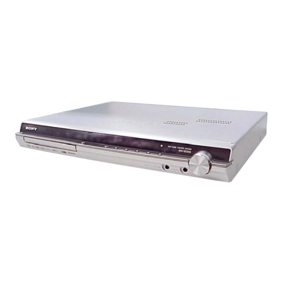
Photo : HCD-DZ230
Model Name Using Similar Mechanism
Mechanism Type
Optical Pick-up Name
SPECIFICATIONS
Inputs (Analog)
TV/VIDEO (AUDIO IN) Sensitivity: 450/250 mV
AUDIO IN
Sensitivity: 250/125 mV
Outputs (Analog)
Phones
Accepts low-and high-
impedance headphones.
DVD system
Laser
Semiconductor laser
(DVD: λ = 650 nm)
(CD: λ = 790 nm)
Emission duration:
continuous
Signal format system
PAL (DZ230/DZ231),
NTSC (HDZ235)
Tuner section
System
PLL quartz-locked digital
synthesizer
FM tuner section
Tuning range
North American models: 87.5-108.0 MHz (100 kHz
step)
Other models:
87.5-108.0 MHz (50 kHz
step)
Antenna (aerial)
FM wire antenna (aerial)
Antenna (aerial) terminals 75 ohms, unbalanced
Intermediate frequency
10.7 MHz
US Model
Canadian Model
HCD-HDZ235
AEP Model
UK Model
HCD-DZ230/DZ231
HCD-DZ110
CDM85-DVBU102
KHM-313CAA
AM tuner section
Tuning range
North American models: 530 – 1,710 kHz (with the
interval set at 10 kHz)
531 – 1,710 kHz (with the
interval set at 9 kHz)
European models:
531 – 1,602 kHz (with the
interval set at 9 kHz)
Antenna (aerial)
AM loop antenna (aerial)
Intermediate frequency
450 kHz
Video section
Outputs:
DZ230/DZ231:
VIDEO: 1 Vp-p 75 ohms
R/G/B: 0.7 Vp-p 75 ohms
HDMI OUT: Type A (19
pin)
HDZ235:
VIDEO: 1 Vp-p 75 ohms
S VIDEO:
Y: 1 Vp-p 75 ohms
C: 0.286 Vp-p 75 ohms
COMPONENT:
Y: 1 Vp-p 75 ohms
P
/C
, P
B
B
R
75 ohms
HDMI OUT: Type A (19
pin)
— Continued on next page —
DVD RECEIVER
/C
: 0.7 Vp-p
R
Advertisement
Table of Contents

Related Manuals for Sony HCD-DZ230


Summary of Contents for Sony HCD-DZ230
-
Page 1: Service Manual
AEP Model Ver. 1.1 2007.03 UK Model HCD-DZ230/DZ231 Photo : HCD-DZ230 HCD-DZ230/DZ231/HDZ235 are the amplifier, DVD/CD and tuner section in DAV-DZ230/DZ231/HDZ235. This system incorporates with Dolby* Digital and Dolby Pro Logic (II) Model Name Using Similar Mechanism HCD-DZ110 adaptive matrix surround decoder and the DTS** Digital Surround System. - Page 2 LES DIAGRAMMES SCHÉMATIQUES ET LA LISTE DES PIÈCES SONT CRITIQUES POUR LA SÉCURITÉ DE FONCTIONNEMENT. NE REMPLACER CES COM- POSANTS QUE PAR DES PIÈCES SONY DONT LES NUMÉROS SONT DONNÉS DANS CE MANUEL OU DANS LES SUPPLÉMENTS PUBLIÉS PAR SONY.
- Page 3 Although this is not a Ordinary soldering irons can be used but the iron tip has to be malfunction and for Sony service use only, applied to the solder joint for a slightly longer time. normal system operation will not be possible.
-
Page 4: Table Of Contents
HCD-DZ230/DZ231/HDZ235 TABLE OF CONTENTS SERVICING NOTE 6-10. Schematic Diagram – MAIN Board (3/9) – ....39 ........... 5 6-11. Schematic Diagram – MAIN Board (4/9) – ....40 6-12. Schematic Diagram – MAIN Board (5/9) – ....41 GENERAL ..............9 6-13. -
Page 5: Servicing Note
HCD-DZ230/DZ231/HDZ235 SECTION 1 SERVICING NOTE Note about CDs/DVDs NOTES ON HANDLING THE OPTICAL PICK-UP BLOCK The system can play CD-ROMs/CD-Rs/CD-RWs recorded in the OR BASE UNIT following formats: – audio CD format The laser diode in the optical pick-up block may suffer electrostatic –... - Page 6 HCD-DZ230/DZ231/HDZ235 How to open the disc table when power switch turns off Insert a tapering driver into the aperture of the unit bottom, and slide it in the direction of the arrow. Peel off the seal and so the lever is moved in the direction of the arrow with the thin rod.
- Page 7 Parts that require fixing using adhesive agent The following parts on the POWER board and on the MAIN board must be fixed by using the adhesive agent (such as Sony Bond Master) as it is specified by Safety Regulations. When any part or printed circuit board is replaced during repair work, be sure to confirm that the following capacitors and resistors are fixed by using the adhesive agent (such as Sony Bond Master) without fail.
- Page 8 HCD-DZ230/DZ231/HDZ235 Precaution when installing a new OP unit / Precaution before unsoldering the static electricity prevention solder bridge When installing a new OP unit, be sure to connect the flexible printed circuit board first of all before removing the static electricity prevention solder bridge by unsoldering.
-
Page 9: General
HCD-DZ230/DZ231/HDZ235 SECTION 2 GENERAL Front panel A "/1 (on/standby) G VOLUME control B A (open/close) H PHONES jack C Disc operation I AUDIO IN/A.CAL MIC jack D FUNCTION J Disc tray E Front panel display (remote sensor) Rear panel DZ230/DZ231... - Page 10 HCD-DZ230/DZ231/HDZ235 Front panel display About the indications in the front panel display HDZ235 only A Lights up when the HDMI OUT jack is I Current repeat mode correctly connected to HDCP (high- J Lights up when the child lock function bandwidth digital content protection) is set to on.
-
Page 11: Remote Control
HCD-DZ230/DZ231/HDZ235 Remote control ALPHABETICAL ORDER BUTTON DESCRIPTIONS [/1 (on/standby) 1 A – O P – Z TV [/1 (on/standby) ej ANGLE 5 PICTURE NAVI 6 C/X/x/c/ AUDIO 4 PRESET +/– wk es REPLAY/ CLEAR ef SOUND FIELD qh ADVANCE 9 D.TUNING wf... -
Page 12: Disassembly
HCD-DZ230/DZ231/HDZ235 SECTION 3 DISASSEMBLY 3-1. DISASSEMBLY FLOW • This set can be disassembled in the order shown below. 3-2. CASE (DS), FRONT PANEL ASSY (Page 13) 3-5. DMPORT BOARD 3-11. DVD MECHANISM 3-9. SPEAKER BOARD, 3-3. FL BOARD (DZ230/DZ231), DECK D.C. -
Page 13: Case (Ds), Front Panel Assy
HCD-DZ230/DZ231/HDZ235 Note: Follow the disassembly procedure in the numerical order given. 3-2. CASE (DS), FRONT PANEL ASSY 5 two screws (CASE3 TP2) Route the harness as shown below. 7 five screws (+BVTP 3 × 8) harness notch 8 case (DS) -
Page 14: Fl Board
HCD-DZ230/DZ231/HDZ235 3-3. FL BOARD 7 wire (flat type) 21core (CN801) 6 wire (flat type) 13core (CN805) 8 FL board 5 two screws (+BVTP 2.6 × 10) 4 shield plate (FR) 3 five screws (+BVTP 2.6 × 10) 2 retainer (DS) -
Page 15: Jack Board, P-Sw Board
HCD-DZ230/DZ231/HDZ235 3-4. JACK BOARD, P-SW BOARD 7 button (AIO) q; P- SW board 6 screw (+BVTP 2.6 × 10 ) 9 harness 1 knob (vol) 4 button (AIO) 2 nut 5 wire (flat type) 13core (CNP806) 8 Remove the solderings. -
Page 16: Io-Scart Board (Dz230/Dz231)
HCD-DZ230/DZ231/HDZ235 3-6. IO-SCART BOARD (DZ230/DZ231) 8 wire (flat type) 6 three screws (+BV 3 × 6 ) 11core (CN305) 7 wire (flat type) 9core (CN301) 9 IO-SCART board 5 two screws (+BVTP 3 × 8 ) 4 connector 4p (CN302) -
Page 17: Power Board
HCD-DZ230/DZ231/HDZ235 3-8. POWER BOARD 1 connector Clamp the harnesses with a 6 seven screws 4p (CN3002) (+PWH 3 × 8 ) lead pin or a similar tool so that they do not touch this screw and the heatsink (AMP). lead pin heatsink (AMP) q;... -
Page 18: Main Board
HCD-DZ230/DZ231/HDZ235 3-10. MAIN BOARD 6 screw (+BVTP 3 × 12) Attaching the two radiation sheets 5 two screws (+BV 3 × 10) on the IC MAIN board first, and then attach the heatsink (AMP). 7 heatsink (AMP), HEATSINK B board,... -
Page 19: Dvd Mechanism Deck (Cdm85-Dvbu102)
HCD-DZ230/DZ231/HDZ235 3-11. DVD MECHANISM DECK (CDM85-DVBU102) 1 wire (flat type) 9 three screws (+BV 3 × 6) 2 unweaved 5core (CN307) cloth q; cover (MD) 3 Remove the wire. 8 Remove the wire and harness. qa three screws (+BV 3 × 6) -
Page 20: Belt, Ms-203 Board
HCD-DZ230/DZ231/HDZ235 3-13. BELT, MS-203 BOARD 2 chuck cam 3 belt 4 screw (M 1.7 × 2.5) 1 two claws 7 MS-203 board 6 DC motor 5 three claws... -
Page 21: Optical Pick-Up (Khm-313Caa)
HCD-DZ230/DZ231/HDZ235 3-14. OPTICAL PICK-UP (KHM-313CAA) 3 two claws 2 chuck cam 1 two claws 4 base unit 8 two insulators 6 four insulator screws 9 two insulators 0 optical pick-up (KHM-313CAA) 5 two claws 7 bu holder... -
Page 22: Test Mode
HCD-DZ230/DZ231/HDZ235 SECTION 4 TEST MODE 3. Disc Tray Lock Note: Incorrect operations may be performed if the test mode is not The disc tray lock function for the antitheft of an demonstration entered properly. disc in the store is equipped. - Page 23 HCD-DZ230/DZ231/HDZ235 (2) Select “2. Drive Manual Operation” by pressing the 2 button DVD SECTION on the remote commander. The screen will appear as shown. 7-1. GENERAL DESCRIPTION Drive Manual Operation The IOP measurement allows you to make diagnosis and adjustment 1.
- Page 24 HCD-DZ230/DZ231/HDZ235 7-4. EMERGENCY HISTORY 52: Open kick spindle error To check the emergency history, please follow the following 51: Spindle stop error procedure. 60: Focus on error 61: Seek fail error (1) From the Top Menu of Remocon Diagnosis Menu, select “3.
- Page 25 HCD-DZ230/DZ231/HDZ235 7-4-4. Return to the Top Menu of Remocon Diagnosis 8. DEMO PLAY OUT Menu It is a mode to release the demonstration reproduct by the dedicated Press 0 button on the remote commander. demonstration disc. 1. During playback the DEMO Disc, press the x and H •...
- Page 26 HCD-DZ230/DZ231/HDZ235 11. PROTECTION FACTOR (SD DETECTION/ DC DETECTION) IDENTIFICATION TEST MODE When an error is detected, the FL tube alternately displays “PROTECTOR h PUSH POWER”. Press the button. * Buttons other than the button are invalid. “STANDBY” blinks three times on the FL tube.
-
Page 27: Electrical Adjustment
HCD-DZ230/DZ231/HDZ235 Ver. 1.1 SECTION 5 ELECTRICAL ADJUSTMENT DVD SECTION When the optical pick-up assy is replaced, perform the “EXECUTING IOP MEASUREMENT”. EXECUTING IOP MEASUREMENT (See page 23) TUNER SECTION [FM Tune Level Check] generator OUT (75 Ω ) Procedure: 1. Turn the power on. -
Page 28: Diagrams
HCD-DZ230/DZ231/HDZ235 SECTION 6 DIAGRAMS THIS NOTE IS COMMON FOR PRINTED WIRING BOARDS AND SCHEMATIC DIAGRAMS. (In addition to this, the necessary note is printed in each block.) For Schematic Diagrams. For Printed Wiring Boards. Note: Note: • All capacitors are in µF unless otherwise noted. (p: pF) •... - Page 29 HCD-DZ230/DZ231/HDZ235 • Circuit Boards Location • Waveforms – IO-SCART Board (DZ230/DZ231) – – MAIN Board – IC1101 6 (DVDRFIP) IC230 wf (CYOUTa) 1.7 Vp-p 900 mVp-p 500 mV/DIV, 20 µ s/DIV 200 mV/DIV, 100 ns/DIV DMPORT board IC1101 (XTALI) <xcv...
-
Page 30: Block Diagram - Rf Section
HCD-DZ230/DZ231/HDZ235 6-1. BLOCK DIAGRAM – RF SECTION – CN1105 RFMON V2REFO DVDRFIP V2REFO TO DIAG JIG DVDA AD-IN DVDB ADIN DETECTOR ACLK DVDC AUDIO ALRCK DVDD SECTION ABCK (Page 32) IC4501 BUFFER AMP_MCKO ACLK 8 NA AMP_LRCKO ALRCK 9 NB... -
Page 31: Block Diagram - Video Section
HCD-DZ230/DZ231/HDZ235 6-2. BLOCK DIAGRAM – VIDEO SECTION – DZ230,DZ231 IC230 VIDEO AMP, 75Ω DRIVER J230(1/2) 11 CYIN CrOUT 13 CBIN CYOUT CRIN CbOUT 6 CVBSIN IC202 EURO AV SELECTOR OUT PUT(TO TV) VOUT 6 IN1 MUTE1 CVBSOUT Q279 AUDIO MUTE2... -
Page 32: Block Diagram - Audio Section
HCD-DZ230/DZ231/HDZ235 6-3. BLOCK DIAGRAM – AUDIO SECTION – IC303 AUDIO INPUT SELECTOR (DZ230,DZ231) (HDZ235) IC306 L-CH 14 X1 (DZ230,DZ231) L-CH IC401 IC772 15 X2 (HDZ235) A/D CONVERTER L-CH 12 X0 AD-IN – 13 VINL J401 DOUT – L-CH ALRCK LRCK AUDIO IN/A.CAL MIC... -
Page 33: Block Diagram - Amp Section
HCD-DZ230/DZ231/HDZ235 6-4. BLOCK DIAGRAM – AMP SECTION – IC3001 COMPARATOR J402 – PHONES – PLUG DET2 • Signal Path Q450,451 : AUDIO HPMUTE Q3081 Q460,461 MUTE SW MUTE IC3030 IC3400 S-MASTER PROCESSOR SPEAKER S-MASTER DIGITAL AMP AMP_D1-D3 AMP_BCK0,LRCK0,MCK0 AMP_D3 31 DATA... -
Page 34: Block Diagram - Power Section
HCD-DZ230/DZ231/HDZ235 6-5. BLOCK DIAGRAM – POWER SECTION – POWER Thermistor F901 T901 D901 TRANSFORMER(MAIN) AC IN LINE T801 IC901 FILTER DC/DC POWER CONVERTER D931 PROTECTION D905 +31.5V Q901 TO FLUORESCENT VOLTAGE INDICATOR TUBE CONTROLLER IC931 VOLTAGE OCP/SYNC RECT DETECT PC901... -
Page 35: Printed Wiring Board - Main Board (Side A)
HCD-DZ230/DZ231/HDZ235 • See page 29 for Circuit Boards Location. 6-6. PRINTED WIRING BOARD – MAIN BOARD (SIDE A) – :Uses unleaded solder. • Semiconductor MAIN BOARD (SIDE A) Location HDMI OUT (DVD ONLY) Ref. No. Location CL455 CL462 D501 CN1701... -
Page 36: Printed Wiring Board - Main Board (Side B)
HCD-DZ230/DZ231/HDZ235 • See page 29 for Circuit Boards Location. 6-7. PRINTED WIRING BOARD – MAIN BOARD (SIDE B) – :Uses unleaded solder. MAIN BOARD (SIDE B) SPEAKER CENTER WOOFER – – (CHASSIS) (CHASSIS) • Semiconductor Location C3904 CL459 (CHASSIS) Ref. No. -
Page 37: Schematic Diagram - Main Board (1/9)
HCD-DZ230/DZ231/HDZ235 • See page 29 for Waveforms. • See page 62 for IC Pin Function Description. 6-8. SCHEMATIC DIAGRAM – MAIN BOARD (1/9) – PWON MAIN BOARD (8/9) (Page 44) MAIN BOARD (1/9) SPDIF MAIN BOARD (8/9) (Page 44) ASDATA4... -
Page 38: Schematic Diagram - Main Board (2/9)
HCD-DZ230/DZ231/HDZ235 • See page 58, 59 for IC Block Diagrams. 6-9. SCHEMATIC DIAGRAM – MAIN BOARD (2/9) – MAIN BOARD (2/9) FL4501 C4501 C4502 0.01 R4521 JL4511 D-GND TP708 R4514 TP707 ICT517 FRONT ADIN AMP_D1 MAIN BOARD CL100 R4515 TP706... -
Page 39: Schematic Diagram - Main Board (3/9)
HCD-DZ230/DZ231/HDZ235 • See page 29 for Waveform. • See page 67 for IC Pin Function Description. 6-10. SCHEMATIC DIAGRAM – MAIN BOARD (3/9) – MAIN BOARD (2/9) (Page 38) MAIN BOARD (3/9) DZ230,DZ231 R540 R586 R554 DZ230,DZ321 R555 DZ230,DZ321 R543... -
Page 40: Schematic Diagram - Main Board (4/9)
HCD-DZ230/DZ231/HDZ235 6-11. SCHEMATIC DIAGRAM – MAIN BOARD (4/9) – MAIN BOARD MAIN BOARD (3/9) (3/9) (Page 39) (Page 39) 67 66 64 63 57 56 54 53 MAIN BOARD MAIN BOARD (4/9) HPMUTE (7/9) (Page 43) A.CAL OUT CSFLAG DC-DET... -
Page 41: Schematic Diagram - Main Board (5/9)
HCD-DZ230/DZ231/HDZ235 • See page 58 for IC Block Diagram. 6-12. SCHEMATIC DIAGRAM – MAIN BOARD (5/9) – (CHASSIS) MAIN BOARD (5/9) SL3001 TP3007 DC-DET R3065 TP3003 DIAG JL3060 C3071 0 . 0 1 R3552 TP3004 R3066 Q3551 2SC3052EF-T1-LEF 3 . 3... -
Page 42: Schematic Diagram - Main Board (6/9)
HCD-DZ230/DZ231/HDZ235 • See page 58 for IC Block Diagram. 6-13. SCHEMATIC DIAGRAM – MAIN BOARD (6/9) – MAIN BOARD (5/9) (Page 41) MAIN BOARD (6/9) IC3250 C3256 S-MASTER 0 . 0 3 3 DIGITAL AMP JL3056 Q3202 2SA1235TP-1EF 3 1 . 3... -
Page 43: Schematic Diagram - Main Board (7/9)
HCD-DZ230/DZ231/HDZ235 • See page 29 for Waveform. • See page 58 for IC Block Diagram. 6-14. SCHEMATIC DIAGRAM – MAIN BOARD (7/9) – MAIN BOARD MAIN (6/9) BOARD (Page 42) (5/9) (Page 41) MAIN BOARD (7/9) SOFTMUTE PGMUTE IC3150 SC_DT... -
Page 44: Schematic Diagram - Main Board (8/9)
HCD-DZ230/DZ231/HDZ235 • See page 25 for Waveforms. • See page 59 for IC Pin Function Description. 6-15. SCHEMATIC DIAGRAM – MAIN BOARD (8/9) – R1734 MAIN BOARD (8/9) C1717 C1718 0 . 0 1 0 . 0 1 R1740 IC1702 IC1703 +1.8V REG... -
Page 45: Schematic Diagram - Main Board (9/9)
HCD-DZ230/DZ231/HDZ235 • See page 58 for IC Block Diagram. 6-16. SCHEMATIC DIAGRAM – MAIN BOARD (9/9) – MAIN BOARD (9/9) MAIN BOARD (1/9) (Page 37) MAIN BOARD IOPMON (1/9) (Page 37) FCS- MAIN BOARD FCS- SW+5V (1/9) (Page 37) FCS+... -
Page 46: Printed Wiring Board - Ms-203 Board
HCD-DZ230/DZ231/HDZ235 • See page 29 for Circuit Boards Location. 6-17. PRINTED WIRING BOARD – MS-203 BOARD – 6-18. SCHEMATIC DIAGRAM – MS-203 BOARD – :Uses unleaded solder. MS-203 BOARD CN001 S001 (CHUCK/TRAY DETECT) MAIN CN001 BOARD CN1202 M203 (Page 35) -
Page 47: Printed Wiring Board - Io-Scart Board (Dz230/Dz231)
HCD-DZ230/DZ231/HDZ235 • See page 29 for Circuit Boards Location. 6-19. PRINTED WIRING BOARD – IO-SCART BOARD (DZ230/DZ231) – :Uses unleaded solder. IO-SCART BOARD • Semiconductor Location Ref. No. Location J230 D271 EURO AV T OUTPUT (TO TV) D272 D297 D-17... -
Page 48: Schematic Diagram - Io-Scart Board (Dz230/Dz231)
HCD-DZ230/DZ231/HDZ235 • See page 29 for Waveforms. • See page 59, 60 for IC Block Diagrams. 6-20. SCHEMATIC DIAGRAM – IO-SCART BOARD (DZ230/DZ231) – IO-SCART BOARD IC303 CN302 R399 AUDIO INPUT SELECTOR JL011 JL010 R398 C373 C375 C377 JACK IPOD(R) -
Page 49: Printed Wiring Board - Io-S-Out Board (Hdz235)
HCD-DZ230/DZ231/HDZ235 • See page 29 for Circuit Boards Location. 6-21. PRINTED WIRING BOARD – IO-S-OUT BOARD (HDZ235) – :Uses unleaded solder. IO-S-OUT BOARD J301 MONITOR OUT J303 • Semiconductor TV/VIDEO S VIDEO Location AUDIO IN COMPONENT (DVD ONLY) VIDEO Ref. No. -
Page 50: Schematic Diagram - Io-S-Out Board (Hdz235)
HCD-DZ230/DZ231/HDZ235 • See page 29 for Waveforms. • See page 59 for IC Block Diagrams. 6-22. SCHEMATIC DIAGRAM – IO-S-OUT BOARD (HDZ235) – IO-S-OUT BOARD C387 CL017 C389 IC307 IC307 TA7809LS +9V REG D309 CN305 R399 R398 RB501V-40TE-17 R403 R406... -
Page 51: Printed Wiring Boards - Fl, Jack Board
HCD-DZ230/DZ231/HDZ235 • See page 29 for Circuit Boards Location. 6-23. PRINTED WIRING BOARDS – FL, JACK BOARD – :Uses unleaded solder. FL BOARD MAIN BOARD CN502 (Page 35) R805 T801 JW829 R804 R801 TP821 TP819 JR802 L802 L801 IC801 CN805... -
Page 52: Schematic Diagram - Fl Board
HCD-DZ230/DZ231/HDZ235 • See page 61 for IC Block Diagram. 6-24. SCHEMATIC DIAGRAM – FL BOARD – FL BOARD ND001 (VACUUM FLUORESCENT DISPLAY) CN805 KEY2 TP851 KEY1 TP852 KEY0 R800 TP853 3.3V T801 L801 D-GND DC/DC CONVERTER D804 D803 47uH 1SS355WTE-17 UDZW-TE17-6.2B... -
Page 53: Schematic Diagram - Jack Board
HCD-DZ230/DZ231/HDZ235 6-25. SCHEMATIC DIAGRAM – JACK BOARD – JACK BOARD R472 TP415 R857 R856 R855 R478 2 . 2 k 2 . 2 k Q473 Q470 RT1P141C-TP-1 S800 RT1N441C-TP-1 S805 S804 CN809 S806 3 . 3 MO/ST DETECT MO/ST DETECT... -
Page 54: Printed Wiring Board
HCD-DZ230/DZ231/HDZ235 • See page 29 for Circuit Boards Location. • See page 61 for IC Block Diagram. 6-26. PRINTED WIRING BOARD – DMPORT BOARD (DZ230/DZ231) – 6-27. SCHEMATIC DIAGRAM – DMPORT BOARD (DZ230/DZ231) – :Uses unleaded solder. DMPORT BOARD (SIDE A) -
Page 55: Printed Wiring Boards - Speaker, P-Sw Board
HCD-DZ230/DZ231/HDZ235 • See page 29 for Circuit Boards Location. 6-28. PRINTED WIRING BOARDS – SPEAKER, P-SW BOARD – 6-29. SCHEMATIC DIAGRAM – SPEAKER, P-SW BOARD – :Uses unleaded solder. SPEAKER BOARD SPEAKER FRONT R FRONT L SUR R SUR L SPEAKER BOARD –... -
Page 56: Printed Wiring Board - Power Board
HCD-DZ230/DZ231/HDZ235 • See page 29 for Circuit Boards Location. 6-30. PRINTED WIRING BOARD – POWER BOARD – :Uses unleaded solder. POWER BOARD DZ230,DZ231 • Semiconductor MAIN DMPORT MAIN BOARD BOARD BOARD Location CN3002 CN203 CN506 (Page 36) (CHASSIS) (Page 54) -
Page 57: Schematic Diagram - Power Board
HCD-DZ230/DZ231/HDZ235 • See page 60 for IC Block Diagram. 6-31. SCHEMATIC DIAGRAM – POWER BOARD – (CHASSIS) (CHASSIS) (CHASSIS) POWER BOARD JW928 EB905 C938 C964 C963 CN901 TH901 F901 HDZ235 FH901 FH902 THERMISTOR, NTC 3.0 TP901 JW981 LIVE C930 NUTRAL C920 0.01... - Page 58 HCD-DZ230/DZ231/HDZ235 • IC Block Diagrams – MAIN Board – IC1201 FAN8036L IC3010, IC3020, IC3030 CXD9843AR FI N (GND) REGVCC IN1- DO1- OVF FLAG L Serial DO2+ OUT1 Control SFLAG INT/MUTE IN2 + DO2- INIT IN2- P GND1 MCKSEL REGVCC REGVCC...
- Page 59 HCD-DZ230/DZ231/HDZ235 – MAIN Board – IC772 PCM1808PWR Serial LRCK Interface DOUT Mode/ Format Control Clock Timing SCKI Control × 1/64 Decimation Filter with HighúPass Filter DGND DeltaúSigma DeltaúSigma Modulator Modulator Power Supply Antialias AGND VINL VREF Reference Antialias VINR – IO-SCART Board (DZ230/DZ231) –...
- Page 60 HCD-DZ230/DZ231/HDZ235 – IO-SCART Board (DZ230/DZ231) – IC230 BH7868FS-E2 6MHz VCC1 75Ω 32 C OUT S-DC OUT 31 S-DC OUT S1/S2 C IN BIAS MUTE1 MUTE1 6MHz 75Ω CV OUT CV IN CLAMP CV OUT SAG SEL (CV/MIX) 6MHz Y IN CLAMP 75Ω...
- Page 61 HCD-DZ230/DZ231/HDZ235 – FL Board – IC802 uPD16315GB-3BS Grid driver Multiplexed driver SEG19/GRID10 Command decoder LED1 SEG18/GRID11 LED2 Display memory LED3 SEG17/GRID12 24 bits x 12 words LED4 Timing generator key scan DOUT SEG16/KS16 Key data memory Serial SEG15/KS15 (2 x 16 bits)
- Page 62 HCD-DZ230/DZ231/HDZ235 • IC Pin Function Description MAIN BOARD IC1101 CXD9889R (CD/DVD RF AMP, FOCUS/TRACKING ERR AMP, DVD SYSTEM PROCESSOR, DIGTAL SERVO PROCESSOR) Pin No. Pin Name Description AGND — Ground terminal DVDA AC coupled input path A DVDB AC coupled input path B...
- Page 63 HCD-DZ230/DZ231/HDZ235 Pin No. Pin Name Description RESERVED — USB port DMINUS pin for HS DL (not used (Open)) USB_VDD3 — Power supply (SW+3.3V) SPFG Spindle FG input DVD/CD switch (H:DVD / L:CD) CKSW CKSW input OCSW OCSW input EEWP EEPROM Write Protect control (L:Write allowed) DVDD18 —...
- Page 64 HCD-DZ230/DZ231/HDZ235 Pin No. Pin Name Description RWE# Write enable output to SDRAM (IC1104) CAS# Column address strobe output to SDRAM (IC1104) RAS# Row address strobe output to SDRAM (IC1104) RCS# Chip select output to SDRAM (IC1104) 137, 138 BA0, 1...
- Page 65 HCD-DZ230/DZ231/HDZ235 Pin No. Pin Name Description TRG_SW Slot-in MECHA Triger SW detect (not used (Fixed to “H” (SW+3.3V))) SCORE Calculation of SCORE (not used (Fixed to Ground)) Detection of MIC signal (H:Voice exist / L:Voice is absence) XVOICE (not used (Fixed to Ground)) Fixed_Low —...
- Page 66 HCD-DZ230/DZ231/HDZ235 Pin No. Pin Name Description RFVDD3 — Power supply (RF+3.3V) RFRPDC RF ripple detect output RFRPAC RF ripple detect input (through AC-coupling) HRFZC High frequency RF ripple zero crossing CRTPLP Defect level filter capacitor connecting RFGND18 — Ground terminal...
- Page 67 HCD-DZ230/DZ231/HDZ235 MAIN BOARD IC501 M30622MEP-B02FPU0 (DZ230/DZ231), M30622MEP-B03FPU0 (HDZ235) (SYSTEM CONTROLLER) Pin No. Pin Name Description DAMP_SCDT/ DAMP processor data output DIAT_SDATA/DIR_DIN DAMP_SHIFT/ DAMP processor clock output DIAT_SCLK/DIR_CLK CEC_RX_IN CEC data input SIRCS_IN Sircs input NO USE Not used (Open) NO USE...
- Page 68 HCD-DZ230/DZ231/HDZ235 Pin No. Pin Name Description DAMP LATCH2 DAMP processor latch2 DAMP LATCH3 DAMP processor latch3 DAMP INIT DAMP processor reset DAMP SOFT MUTE DAMP processor soft muting HP_SW Headphone detect HP_MUTE Headphone muting NO USE Not used (Open) NO USE...
- Page 69 HCD-DZ230/DZ231/HDZ235 Pin No. Pin Name Description MODEL Model select input KEY2 Key input 2 input KEY1 Key input 1 input — Ground terminal KEY0 Key input 0 input VREF — Reference voltage (E3.3V) — Power supply (BUP+3.3V) NO USE Not used...
-
Page 70: Exploded Views
HCD-DZ230/DZ231/HDZ235 SECTION 7 EXPLODED VIEWS NOTE: • -XX and -X mean standardized parts, so they The components identified by mark 0 or The components identified by mark 9 contain may have some difference from the original dotted line with mark 0 are critical for safety. -
Page 71: Front Panel Section
HCD-DZ230/DZ231/HDZ235 7-2. FRONT PANEL SECTION supplied supplied supplied supplied supplied supplied including S800 Ref. No. Part No. Description Remark Ref. No. Part No. Description Remark 2-889-990-01 KNOB (VOL) 2-889-992-01 FILTER, COLOR 2-889-982-01 WINDOW, INDICATION (INJ) (DZ230) 2-889-983-01 BUTTON (AIO) 2-889-982-21 WINDOW, INDICATION (INJ) (HDZ235) 3-087-053-11 +BVTP2.6 (3CR) -
Page 72: Chassis Section
HCD-DZ230/DZ231/HDZ235 7-3. CHASSIS SECTION supplied HCD-HDZ235 supplied supplied supplied HCD-DZ230/DZ231 supplied supplied supplied supplied not supplied HCD-DZ230/DZ231 supplied DVD mechanism F901 deck section (CDM85-DVBU102) not supplied not supplied Ref. No. Part No. Description Remark Ref. No. Part No. Description Remark... -
Page 73: Dvd Mechanism Deck Section (Cdm85-Dvbu102)
HCD-DZ230/DZ231/HDZ235 7-4. DVD MECHANISM DECK SECTION (CDM85-DVBU102) not supplied not supplied not supplied not supplied not supplied not supplied not supplied not supplied supplied Ref. No. Part No. Description Remark Ref. No. Part No. Description Remark A-6071-669-A LOADING ASSY (M) -
Page 74: Electrical Parts List
HCD-DZ230/DZ231/HDZ235 SECTION 8 DMPORT ELECTRICAL PARTS LIST NOTE: • Due to standardization, replacements in the • SEMICONDUCTORS The components identified by mark 9 contain In each case, u: µ, for example: parts list may be different from the parts confidential information. - Page 75 HCD-DZ230/DZ231/HDZ235 IO-SCART Ref. No. Part No. Description Remark Ref. No. Part No. Description Remark < CONNECTOR > A-1218-023-A IO-SCART BOARD, COMPLETE (DZ230/DZ231) ************************ CN801 1-779-558-11 CONNECTOR, FFC (LIF (NON-ZIF)) 21P CN805 1-794-506-51 CONNECTOR, FFC/FPC 13P < CAPACITOR > < DIODE >...
- Page 76 HCD-DZ230/DZ231/HDZ235 IO-SCART IO-S-OUT Ref. No. Part No. Description Remark Ref. No. Part No. Description Remark R285 1-216-833-11 METAL CHIP 1/10W CN308 1-779-289-11 CONNECTOR, FFC (LIF (NON-ZIF)) 21P R303 1-216-864-11 SHORT CHIP R308 1-216-827-11 METAL CHIP 3.3K 1/10W < DIODE >...
- Page 77 HCD-DZ230/DZ231/HDZ235 IO-S-OUT Ref. No. Part No. Description Remark Ref. No. Part No. Description Remark C228 1-126-916-11 ELECT 1000uF 6.3V < JACK > C251 1-162-964-11 CERAMIC CHIP 0.001uF C302 1-162-964-11 CERAMIC CHIP 0.001uF J301 1-694-920-11 TERMINAL BOARD (S TERMINAL+1P) C311 1-162-960-11 CERAMIC CHIP...
- Page 78 HCD-DZ230/DZ231/HDZ235 IO-S-OUT JACK Ref. No. Part No. Description Remark Ref. No. Part No. Description Remark R412 1-218-827-11 METAL CHIP 0.5% 1/10W FB479 1-500-236-22 BEAD, FERRITE (CHIP) (1608) R413 1-218-827-11 METAL CHIP 0.5% 1/10W < IC > R414 1-216-864-11 SHORT CHIP...
- Page 79 HCD-DZ230/DZ231/HDZ235 JACK MAIN Ref. No. Part No. Description Remark Ref. No. Part No. Description Remark R470 1-216-825-11 METAL CHIP 2.2K 1/10W C527 1-126-916-11 ELECT 1000uF 6.3V R471 1-216-825-11 METAL CHIP 2.2K 1/10W C528 1-126-916-11 ELECT 1000uF 6.3V R472 1-216-819-11 METAL CHIP...
- Page 80 HCD-DZ230/DZ231/HDZ235 MAIN Ref. No. Part No. Description Remark Ref. No. Part No. Description Remark C1153 1-162-916-11 CERAMIC CHIP 12PF C1602 1-128-994-21 ELECT CHIP 47uF C1154 1-107-826-11 CERAMIC CHIP 0.1uF C1603 1-128-994-21 ELECT CHIP 47uF C1155 1-162-970-11 CERAMIC CHIP 0.01uF C1156 1-162-970-11 CERAMIC CHIP 0.01uF...
- Page 81 HCD-DZ230/DZ231/HDZ235 MAIN Ref. No. Part No. Description Remark Ref. No. Part No. Description Remark C3116 1-112-831-11 ELECT 2200uF C3027 1-107-826-11 CERAMIC CHIP 0.1uF C3122 1-162-964-11 CERAMIC CHIP 0.001uF C3028 1-107-826-11 CERAMIC CHIP 0.1uF C3123 1-162-964-11 CERAMIC CHIP 0.001uF C3029 1-107-826-11 CERAMIC CHIP 0.1uF...
- Page 82 HCD-DZ230/DZ231/HDZ235 MAIN Ref. No. Part No. Description Remark Ref. No. Part No. Description Remark < DIODE > C3312 1-112-246-11 ELECT 100uF C3313 1-104-329-11 CERAMIC CHIP 0.1uF D501 6-501-193-01 DIODE 1SS355WTE-17 C3314 1-136-177-00 FILM D502 6-501-193-01 DIODE 1SS355WTE-17 C3315 1-136-177-00 FILM...
- Page 83 HCD-DZ230/DZ231/HDZ235 MAIN Ref. No. Part No. Description Remark Ref. No. Part No. Description Remark FL4501 1-234-177-21 FILTER, CHIP EMI L3402 1-456-680-11 INDUCTOR 10uH L3901 1-457-077-11 AIR-CORE COIL < IC > L3902 1-457-078-11 AIR-CORE COIL IC501 6-807-087-01 IC M30622MEP-B02FPU0 (DZ230/DZ231) L3903...
- Page 84 HCD-DZ230/DZ231/HDZ235 MAIN Ref. No. Part No. Description Remark Ref. No. Part No. Description Remark R509 1-216-809-11 METAL CHIP 1/10W R586 1-216-833-11 METAL CHIP 1/10W R510 1-216-833-11 METAL CHIP 1/10W R587 1-216-833-11 METAL CHIP 1/10W R511 1-216-821-11 METAL CHIP 1/10W R512...
- Page 85 HCD-DZ230/DZ231/HDZ235 MAIN Ref. No. Part No. Description Remark Ref. No. Part No. Description Remark R1109 1-216-864-11 SHORT CHIP R1216 1-216-834-11 METAL CHIP 1/10W R1110 1-216-841-11 METAL CHIP 1/10W R1219 1-216-838-11 METAL CHIP 1/10W R1220 1-216-821-11 METAL CHIP 1/10W R1111 1-216-809-11 METAL CHIP...
- Page 86 HCD-DZ230/DZ231/HDZ235 MAIN Ref. No. Part No. Description Remark Ref. No. Part No. Description Remark R1751 1-216-864-11 SHORT CHIP R2718 1-208-635-11 METAL CHIP 0.5% 1/16W R1752 1-216-864-11 SHORT CHIP R2751 1-216-833-11 METAL CHIP 1/10W R3001 1-216-833-11 METAL CHIP 1/10W R1753 1-216-864-11 SHORT CHIP...
- Page 87 HCD-DZ230/DZ231/HDZ235 MAIN Ref. No. Part No. Description Remark Ref. No. Part No. Description Remark R3079 1-216-809-11 METAL CHIP 1/10W R3301 1-216-809-11 METAL CHIP 1/10W R3080 1-216-845-11 METAL CHIP 100K 1/10W R3302 1-216-809-11 METAL CHIP 1/10W R3303 1-216-864-11 SHORT CHIP R3085...
- Page 88 HCD-DZ230/DZ231/HDZ235 MAIN MS-203 POWER Ref. No. Part No. Description Remark Ref. No. Part No. Description Remark R4706 1-216-864-11 SHORT CHIP A-1218-005-A POWER BOARD, COMPLETE (DZ230/DZ231) R4717 1-216-864-11 SHORT CHIP 0 (HDZ235) A-1228-785-A POWER BOARD, COMPLETE (HDZ235) *********************** R4718 1-216-864-11 SHORT CHIP...
- Page 89 HCD-DZ230/DZ231/HDZ235 POWER Ref. No. Part No. Description Remark Ref. No. Part No. Description Remark C948 1-126-925-91 ELECT 470uF < TERMINAL BOARD > C949 1-104-658-91 ELECT 100uF C951 1-100-566-91 CERAMIC CHIP 0.1uF EB901 1-537-770-21 TERMINAL BOARD, GROUND C952 1-100-756-91 CERAMIC CHIP 0.047uF...
- Page 90 HCD-DZ230/DZ231/HDZ235 POWER P-SW SPEAKER Ref. No. Part No. Description Remark Ref. No. Part No. Description Remark 0 R904 1-215-926-00 METAL OXIDE R966 1-216-821-11 METAL CHIP 1/10W (HDZ235) R967 1-216-821-11 METAL CHIP 1/10W 0 R904 1-215-929-11 METAL OXIDE 100K (DZ230/DZ231) R968...
- Page 91 HCD-DZ230/DZ231/HDZ235 SPEAKER Ref. No. Part No. Description Remark < TERMINAL > TB301 1-780-454-11 TERMINAL BOARD (SPEAKER) 4P (SPEAKER FRONT R/FRONT L/SUR R/SUR L) ************************************************************* MISCELLANEOUS ************** 1-828-307-51 WIRE (FLAT TYPE)(9 CORE) (DZ230/DZ231) 1-828-952-51 WIRE (FLAT TYPE)(9 CORE) (HDZ235) 1-828-962-51 WIRE (FLAT TYPE)(11 CORE) (DZ230/DZ231)
-
Page 92: Revision History
HCD-DZ230/DZ231/HDZ235 REVISION HISTORY Clicking the version allows you to jump to the revised page. Also, clicking the version at the upper right on the revised page allows you to jump to the next revised page. Ver. Date Description of Revision 2007.01...
Need help?
Do you have a question about the HCD-DZ230 and is the answer not in the manual?
Questions and answers