Yamaha T3n Service Manual
Hide thumbs
Also See for T3n:
- Owner's manual (15 pages) ,
- Service manual (107 pages) ,
- Owner's manual (19 pages)
Table of Contents
Advertisement
www.freeservicemanuals.info
このサービスマニュアルはエコパルプ
(ECF:無塩素系漂白パルプ)を使用しています。
This document is printed on chlorine free (ECF) paper.
PA
011844
T5n: 200612-682500
T4n: 200612-577500
T3n: 200612-504000
SERVICE MANUAL
I CONTENTS (目次)
SPECIFICATIONS (総合仕様) .................................................................. 3/5
DIMENSIONS (寸法図).............................................................................. 7
PANEL LAYOUT (パネルレイアウト) ......................................................... 8
CIRCUIT BOARD LAYOUT (ユニットレイアウト).................................... 9
DISASSEMBLY PROCEDURES (分解手順) ............................................. 10
LSI PIN DESCRIPTION (LSI端子機能表) .................................................. 18
IC BLOCK DIAGRAM (ICブロック図) ...................................................... 20
CIRCUIT BOARDS (シート基板図) ........................................................... 23
INSPECTIONS (検査) .......................................................................... 36/45
(PSTシート故障修理ガイド) ................................................................ 54/59
IC & DIODE FIGURES (外形図)
BLOCK DIAGRAM (ブロックダイアグラム)
CIRCUIT DIAGRAM (回路図)
Copyright (c) Yamaha Corporation. All rights reserved.
Free World of Manuals
T5n
T4n
T3n
HAMAMATSU, JAPAN
06.12
Advertisement
Table of Contents

Related Manuals for Yamaha T3n


Summary of Contents for Yamaha T3n
-
Page 1: Table Of Contents
PARTS LIST IC & DIODE FIGURES (外形図) このサービスマニュアルはエコパルプ (ECF:無塩素系漂白パルプ)を使用しています。 BLOCK DIAGRAM (ブロックダイアグラム) This document is printed on chlorine free (ECF) paper. CIRCUIT DIAGRAM (回路図) 011844 T5n: 200612-682500 HAMAMATSU, JAPAN T4n: 200612-577500 Copyright (c) Yamaha Corporation. All rights reserved. 06.12 T3n: 200612-504000... -
Page 2: Important Notice
IMPORTANT NOTICE This manual has been provided for the use of authorized Yamaha Retailers and their service personnel. It has been assumed that basic service procedures inherent to the industry, and more specifically Yamaha Products, are already known and understood by the users, and have therefore not been restated. -
Page 3: Specifications (総合仕様
Free World of Manuals T5n/T4n/T3n SPECIFICATIONS... - Page 4 Free World of Manuals T5n/T4n/T3n...
- Page 5 Free World of Manuals T5n/T4n/T3n ■ 総合仕様...
- Page 6 Free World of Manuals T5n/T4n/T3n...
-
Page 7: Dimensions (寸法図
Free World of Manuals T5n/T4n/T3n DIMENSIONS (寸法図) Unit: mm 単位:mm... -
Page 8: Panel Layout (パネルレイアウト
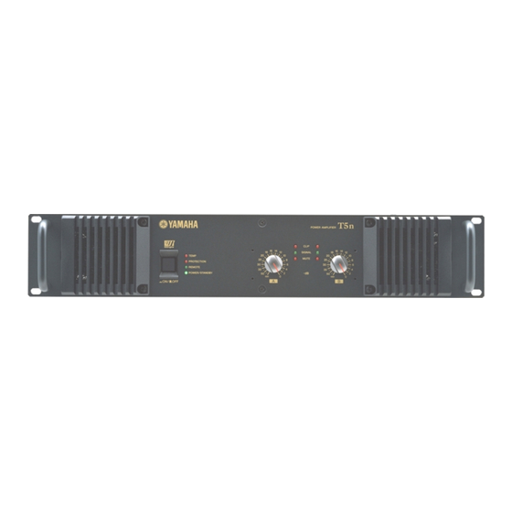
Free World of Manuals T5n/T4n/T3n PANEL LAYOUT (パネルレイアウト) • Front Panel (フロントパネル) 1 TEMPインジケーター 1 TEMP indicator 2 SIGNALインジケーター 2 SIGNAL indicator 3 CLIPインジケーター 3 CLIP indicator 4 Screw holes for handles 4 ハンドル用ネジ穴 5 吸気口 5 Air intakes 6 POWERスイッチ... -
Page 9: Circuit Board Layout (ユニットレイアウト
Free World of Manuals T5n/T4n/T3n CIRCUIT BOARD LAYOUT (ユニットレイアウト) T5n model INSWT5 INSWT4 T4n model INSWT3 T3n model Rear INT5 CPUT5 INT4 CPUT4 INT3 CPUT3 PAT5 PAT5 PAT5 PAT5 PST5 PAT3 PAT3 PST4 PST3 ATTT5 PSWT5 ATTT4 PSWT4 ATTT3... -
Page 10: Disassembly Procedures (分解手順
Free World of Manuals T5n/T4n/T3n DISASSEMBLY PROCEDURES (分解手順) トップカバー (所要時間:約3分) Top Cover (Time required: about 3 minutes) Remove the nine (9) screws marked [320]. The top cover [320] のネジ9本を外し、トップカバーを外します。 can then be removed. (Fig. 1) (Fig. 1) [320] [320]... - Page 11 Free World of Manuals T5n/T4n/T3n PAユニット左側 (所要時間:約6分) PA unit on the left side (Time required: about 6 minutes) トップカバーを外します。 (1項参照) [230A] のネジ3本、 [250A] のネジ3本、 [280A] のネジ2 Remove the top cover. (See Procedure 1.) 本を外し、PAユニット (サイドカバーL、リアアングル Remove the three (3) screws marked [230A], three (3) 付き)...
- Page 12 Free World of Manuals T5n/T4n/T3n PA unit (PAユニット) Rear angle Rear angle (リアアングル) (リアアングル) [180A] [180B] [190A] [190B] [195B] [195A] [180A] [180B] [196A] [196B] [195A] [195B] [190A] [190B] Side cover L Side cover R (サイドカバーL) (サイドカバーR) [180A]: Washer 4x9x0.8 MFZN2W3 (WF578000) 平座みがき丸...
- Page 13 The INT4 circuit board can then be removed. (T4n) (Fig. 5) INT3シートを外します。 (T3n) ( Fig. 5) The INT3 circuit board can then be removed. (T3n) (Fig. 5) [30] のネジ2本を外します。 (Fig. 5) Remove the two (2) screws marked [30]. (Fig. 5) INSWT5シートを外します。...
- Page 14 Free World of Manuals T5n/T4n/T3n フロントAss'y ( 所要時間:約5分) Front Assembly (Time required: about 5 minutes) トップカバーを外します。 (1項参照) [250] のネジ6本 (右側3本、左側3本) 、 [260] のネジ2本 Remove the top cover. (See Procedure 1.) を外し、フロントAss'yを外します。 (Fig. 6) Remove the six (6) screws marked [250] (3 on the left and 3 on the right) and two (2) screws marked [260].
- Page 15 PSWT4 Circuit Board, FPT4 Circuit Board, PSWT3シート、FPT3シート、ATTT3シート (T3n) ATTT4 Circuit Board (T4n) (所要時間:約15分) PSWT3 Circuit Board, FPT3 Circuit Board, トップカバーを外します。 (1項参照) ATTT3 Circuit Board (T3n) フロントAss'yを外します。 (6項参照) [200A] のネジ2本を外し、左側のグリルとフィルターを (Time required: about 15 minutes) 外します。 (Fig. 8) Remove the top cover. (See Procedure 1.) [200B]...
- Page 16 The PSWT4 circuit board can then be removed. (T4n) PSWT3シートを外します。 (T3n) ( Fig. 9) (Fig. 9) [120] のネジ2本を外します。 (Fig. 9) The PSWT3 circuit board can then be removed. (T3n) FPT5シートを外します。 (T5n) ( Fig. 9) (Fig. 9) FPT4シートを外します。 (T4n) ( Fig. 9)...
- Page 17 CPUT3シートを外します。 (T3n) ( Fig. 10) The CPUT5 circuit board can then be removed. (T5n) (Fig. 10) The CPUT4 circuit board can then be removed. (T4n) (Fig. 10) The CPUT3 circuit board can then be removed. (T3n) (Fig. 10) CPUT5 [40] CPUT4...
-
Page 18: Lsi Pin Description (Lsi端子機能表
Free World of Manuals T5n/T4n/T3n LSI PIN DESCRIPTION (LSI端子機能表) • YAC526-EZE2 (X5574A00) DIGITAL VOLUME INT: IC408 NAME FUNCTION ZCEN1 Zero-cross control input 1. Select one from four types of zero-cross modes including nonzero cross mode. When changing zero-cross modes during operation, set the system so that it changes at 1 second or more after the rise of CSN signal. - Page 19 Free World of Manuals T5n/T4n/T3n • HD64F7044F28V (X5719E00) CPU CPUT: IC801 NAME FUNCTION NAME FUNCTION PE1/TIOC4C/DACK0/AH Port E / MTU I/O / DMA transfer strobe / Address hold PD11/D11 PE15/ T I O C4D/ D ACK1/ I R QOUT...
-
Page 20: Ic Block Diagram (Icブロック図
Free World of Manuals T5n/T4n/T3n IC BLOCK DIAGRAM (IC ブロック図) • DS36276M (X2155A00) • IR2110 (X2382A00) Transceiver Driver CPUT: IC802 PST: IC103,104 DETECT LEVEL PULSE SHIFT FILTER DO/RI LEVEL SHIFT PULSE DO/RI DETECT LEVEL SHIFT DELAY • NJM2068M-D (TE2) (X3505A00) •... - Page 21 Free World of Manuals T5n/T4n/T3n • NJM4558M (TE2) (X5804A00) • UC3525AN (X5952A00) Operational Amplifier Switching Regulator INT: IC601, 604-612 PST: IC101 Reference UVLO Regulator Lockout OUTPUT A INV. INPUT GROUND +DC Voltage To Internal Output A N.I. INPUT Supply...
- Page 22 Free World of Manuals T5n/T4n/T3n • NJM7915FA (XD854A00) • NJM7805FA (XJ607A00) Voltage regulator -15V Voltage regulator +5V PST: IC106 PST: IC107 COMMON INPUT OUTPUT OUTPUT INPUT • M5238AFP (XL669A00) Operational Amplifier INT: IC401 +Vcc R101 Power source Q114 Q108...
-
Page 23: Circuit Boards (シート基板図
Free World of Manuals T5n/T4n/T3n CIRCUIT BOARDS (シート基板図) CONTENTS (目次) • ATTT5/ATTT4/ATTT3 Circuit Board (X7901C0) ......28 • CPUT5/CPUT4/CPUT3 Circuit Board (X7901C0) ......29 • FPT5/FPT4/FPT3 Circuit Board (X7901C0) ......23 • INSWT5/INSWT4/INSWT3 Circuit Board (X7901C0) ......28 • INT5/INT4/INT3 Circuit Board (X7901C0) ...... - Page 24 Free World of Manuals T5n/T4n/T3n • INT5/INT4/INT3 Circuit Board to PAT (Bch) W204 to PST W103 to PAT CN205 to FPT CN101 to PAT (Ach) CN202 Component side (部品側) 2NA-WH37850...
- Page 25 Free World of Manuals T5n/T4n/T3n to INSWT CN401 to PAT (Bch) CN201 to PST CN102 to PAT (Ach) CN201 to CPUT CN801 to PAT (Bch) CN202 Component side (部品側) 2NA-WH37850...
- Page 26 Free World of Manuals T5n/T4n/T3n • INT5/INT4/INT3 Circuit Board Pattern side (パターン側) 2NA-WH37850...
- Page 27 Free World of Manuals T5n/T4n/T3n Pattern side (パターン側) 2NA-WH37850...
- Page 28 Free World of Manuals T5n/T4n/T3n • INSWT5/INSWT4/INSWT3 Circuit Board to INT CN402 GAIN 32dB 26dB Component side (部品側) Pattern side (パターン側) 2NA-WH37850 • ATTT5/ATTT4/ATTT3 Circuit Board to INT CN406 VOLUME Component side (部品側) Pattern side (パターン側) 2NA-WH37850...
- Page 29 Free World of Manuals T5n/T4n/T3n • CPUT5/CPUT4/CPUT3 Circuit Board to INT CN405 Component side (部品側) DATA PORT AMP ID Pattern side (パターン側) 2NA-WH37850...
- Page 30 Free World of Manuals T5n/T4n/T3n • PAT5/PAT3 Circuit Board FOR ADJUSTMENT to INT CN605 to INT CN608 to INT CN603 to INT CN604 FOR ADJUSTMENT to PST CN106 to PST CN109 to PST CN105 to PST CN108 to PST CN107...
- Page 31 Free World of Manuals T5n/T4n/T3n • PSWT5/PSWT4/PSWT3 Circuit Board to PST CN101 (5 pin) to PST CN101 (1 pin) to PST CN101 (3 pin) to PST CN101 (6 pin) POWER ON/OFF Component side (部品側) Pattern side (パターン側) 2NA-WH52830...
- Page 32 Free World of Manuals T5n/T4n/T3n • PST5/PST4/PST3 Circuit Board Reduction: 4/5 to PSWT (1 pin) W101A to PSWT (3 pin) W101B to PSWT (5 pin) W101C to PSWT (6 pin) W101D AC IN Component side (部品側) 2NA-WH52830...
- Page 33 Free World of Manuals T5n/T4n/T3n to PAT W203 to INT CN607 to PAT W202 Reduction: 4/5 to PAT W201 to PAT CN206 to FUN (R) to INT CN602 to FUN (L) to PAT CN206 Component side (部品側) to PAT W203...
- Page 34 Free World of Manuals T5n/T4n/T3n • PST5/PST4/PST3 Circuit Board Reduction: 4/5 Pattern side (パターン側) 2NA-WH52830...
- Page 35 Free World of Manuals T5n/T4n/T3n Reduction: 4/5 Pattern side (パターン側) 2NA-WH52830...
-
Page 36: Inspections (検査
Free World of Manuals T5n/T4n/T3n INSPECTIONS Measurement Conditions 1-1. Environment Normal temperature: From 10 °C to 35 °C. • • Normal humidity: From 45 % to 85 % 1-2. Power Source • When measuring the electrical characteristics, set the power supply voltage and frequency as specified in the table below. - Page 37 Free World of Manuals T5n/T4n/T3n 3-2. Inspection and adjustment 3-2-1. Fan, POWER/PROTECTION/MUTE LED Turn on the POWER switch and check the PROTECTION LED and MUTE LED light in red color and the POWER LED lights in green color. Also check the fans rotate in low speed.
- Page 38 Free World of Manuals T5n/T4n/T3n T3n: 1) Input 1 kHz sine wave to A channel input terminal, adjust the VR601 so that 0.225 ± 0.005 Vrms is obtained between No.1 and No.2 terminal of CN611 when output voltage is 40 Vrms.
- Page 39 Free World of Manuals T5n/T4n/T3n 3-2-11. Channel separation Input the sine wave given in the below table to the input terminal of one channel and measure the output voltage as reference voltage (0 dB). Then, measure the output voltage at the other channel input grounded via 600 ohms resistance and check that it is -65 dB or less as compared with the reference voltage.
- Page 40 Free World of Manuals T5n/T4n/T3n 3-2-15. PC limiter and compressor Connect the 0.5 ohms 500 W resistance to the output terminal. Perform this inspection in the one channel drive state. Input 1 kHz, 0 dBu sine wave to the input terminal, and check the output level is within the range specified in the table below.
- Page 41 Using the keyboard of Windows PC, press the return key once and check that REMOTE LED lights up. The monitor screen appears as shown below (for T5n). MODEL ID:10(T5n)[YAC526] MODEL ID: 10 (T5n), MODEL ID: 11 (T4n), MODEL ID: 12 (T3n)
- Page 42 Free World of Manuals T5n/T4n/T3n 5-3-3. Automatic inspection 1. TEST 10 (STANDBY, PROTECT) Using the keyboard of Windows PC, enter 00 and check that PROTECTION LED lights up and POWER LED lights in orange. (POWER LED lights in orange for about 2 seconds and then changes to green.) The monitor screen appears as shown below and judgment is made automatically.
- Page 43 Free World of Manuals T5n/T4n/T3n 5. TEST 50 (MUTE) The monitor screen appears as shown below and judgment is made automatically. >>50:MUTE TEST MUTE ON VSP(CH A):0.00V-<OK> VSP(CH B):0.00V-<OK> ---------<TEST50:OK> When the TEST 50 result is OK, “---------<TEST50:OK>” appears on the screen.
-
Page 44: Factory Setting
Free World of Manuals T5n/T4n/T3n 8. TEST 80 (MONITOR) The monitor screen appears as shown below and judgment is made automatically. >>80:MONITOR TEST TEMP(CH A):44C-<OK> TEMP(CH B):40C-<OK> Vpre(CH A):1.49V-<OK> Vpre(CH B):1.50V-<OK> VSP(CH A):31.28V-<OK> VSP(CH B):31.08V-<OK> ISP(CH A):4.53A-<OK> ISP(CH B):4.57A-<OK>... - Page 45 Free World of Manuals T5n/T4n/T3n 検査 測定条件 1-1. 環境 ・ 常温:10 ℃∼35 ℃ ・ 常湿:45 %∼85 % 1-2. 電源電圧 ・ 電気的特性の検査の際には電源電圧を100 V +2/-0 %、50 Hzに設定してください。 1-3. 測定器 ・ 検査に使用する測定器は、本文中に記載の規格を十分精度良く測定できる精度及び確度を持つものを使用してください。 ・ 測定器の入力インピーダンスは1 MΩ以上のものを使用してください。 LED点灯検査 CN603から束線TEを引き抜き、図1に示す回路を接続します。 電源を投入した際、PROTECTION LED、TEMP LED、MUTE LEDが赤色に点灯し、POWER LEDが緑色に点灯することを...
- Page 46 Free World of Manuals T5n/T4n/T3n 3-2. 検査及び調整 3-2-1. ファン、POWER/PROTECTION/MUTE LED 電源SW投入時、PROTECTION LED、MUTE LEDが赤色に点灯し、POWER LEDが緑色に点灯することを確認します。 またファンが低速にて回転していることを確認します。 3-2-2. パワーONミューティング時間 電源SW投入後、t=9±3秒にてミューティングが解除され、PROTECTION LED、MUTE LEDが消灯することを確認します。 3-2-3. アイドリング電流 入力端子を接地し、CN204 ( A ch) 、CN203 ( B ch) の1-2番端子の直流電圧Vb=0.1±0.05 mVとなるようにVR201 ( A ch) 、VR202 (B ch) を調整します。...
- Page 47 Free World of Manuals T5n/T4n/T3n T3n: 1)Aチャンネル入力端子に1 kHzの正弦波を入力して、40 Vrmsの出力を得たとき、CN611の1-2ピン間に0.225±0.005 Vrms が得られるようにVR601を調整します。 2)Bチャンネル入力端子に1 kHzの正弦波を入力して、40 Vrmsの出力を得たとき、CN611の3-4ピン間に0.225±0.005 Vrms が得られるようにVR602を調整します。 注意: ・ 入力信号は片ch毎に入力してください。 3-2-9. 歪率 1)入力端子に1 kHzの高品位正弦波を入力し、下表の出力を得たとき歪率が、THD=1.0 %以下であることを確認します。 なお、この検査は30秒以内に終了してください。 1200 W/8 Ω(42.04 dBu/ch) 1000 W/8 Ω(41.24 dBu/ch) 700 W/8 Ω(39.70 dBu/ch) 2)入力端子に、1 kHzの正弦波を入力し、下表の出力を得たとき歪率が、THD=0.1 %以下であることを確認します。...
- Page 48 Free World of Manuals T5n/T4n/T3n 3-2-11.チャネルセパレーション 1つのチャンネルの入力端子に下表の正弦波を入力して得られた出力電圧を基準レベル (0 dB) として、入力端子が600 Ωの 抵抗を介して接地された他方のチャンネルの出力電圧を測定し-65 dB以下であることを確認します。 7.2 dBu 6.4 dBu 4.9 dBu 3-2-12.出力ノイズレベル 1)入力アッテネータを最大、入力端子を600 Ωの抵抗を介して接地し、出力端子に発生するノイズレベルを測定し、-65 dBu 以下であることを確認します。 2)入力アッテネータを最小にし、ノイズレベルは-65 dBu以下であることを確認します。 注意: ・ ノイズレベルはDINオーディオフィルターを使用して測定します。 3-2-13.安定度 1 kHz、-4.0 dBuの矩形波を入力し、負荷を純容量0.1 uFのみとした時、下記の条件を満足することを確認します。 オーバーシュート :Vp/Vo≦2.5 リンギング :7波以内にて収束し発振などを生じないこと。 PART NO.
- Page 49 Free World of Manuals T5n/T4n/T3n 3-2-15.PCリミッター及びコンプ 負荷抵抗を0.5Ω/500 Wに変更します。 この検査は片ch毎行います。 入力端子に1 kHz、0 dBuの正弦波を入力して、下表の出力レベルがえられることを確認します。 また、歪率は下表の条件を満たすことを確認します。 出力レベル 歪率 22.2±2.0 dBu 5 % 以下 22.2±2.0 dBu 5 % 以下 20.4±2.0 dBu 5 % 以下 注意: ・ この検査は30秒以内に終了してください。 3-2-16.SIGNAL LED 1 kHzの正弦波を入力し1 Vrmsの出力を得たときにSIGNAL LEDが点灯していることを確認します。...
- Page 50 入力端子には1 kHz、0 dBの正弦波を入力します。その時、モニタ画面が次の文字を表示する事を確認します。 <<<<< PC-N Series Amplifier Test Program >>>> - FIRMWARE VERSION:V*.** - TEST PROGRAM VERSION:V*.** *.**: バージョン番号 5-3-2. REMOTE、MODEL ID検査 Windows PCのキーボードよりリターンを1回入力します。REMOTE LEDが点灯することを確認します。 そのときモニタ画面が次の文字を表示します。 (下記はT5nの場合です。) MODEL ID:10(T5n)[YAC526] MODEL ID:10 ( T5n) 、MODEL ID:11 ( T4n) , MODEL ID:12 ( T3n)...
- Page 51 Free World of Manuals T5n/T4n/T3n 5-3-3. 自動検査 1. TEST 10検査 (STANDBY、PROTECT) Windows PCのキーボードより00の文字を入力します。 (半角文字) PROTECTION LEDが点灯し、POWER LEDが橙色に点灯します。 (POWER LEDは約2秒間、橙色に点灯し、その後、緑色に変わります。) モニタ画面が次の文字を表示し、自動で判定を行います。 >>00:ALL TEST >>10:POWER TEST Waiting for PROTECTION=NONE... PROTECTION:NONE--<OK> POWER:STANDBY Wait 2sec.. PROTECTION:ON--<OK> POWER:ON ---------<TEST10:OK> TEST 10がOKの場合は “---------<TEST10:OK>” が表示されます。 TEST 10終了後自動でTEST 20に進みます。...
- Page 52 Free World of Manuals T5n/T4n/T3n 5. TEST 50 ( MUTE) モニタ画面が次の文字を表示し、自動で判定を行います。 >>50:MUTE TEST MUTE ON VSP(CH A):0.00V-<OK> VSP(CH B):0.00V-<OK> ---------<TEST50:OK> TEST 50がOKの場合は “---------<TEST50:OK>” が表示されます。 TEST 50終了後自動でTEST 60に進みます。 6. TEST 60 ( MODE SW) モニタ画面が次の文字を表示します。 >>60:MODE SW TEST MODE:STEREO MODE:BRIDGE MODE SWをSTEREO →...
- Page 53 Free World of Manuals T5n/T4n/T3n 8. TEST 80 ( MONITOR) モニタ画面が次の文字を表示し、自動で判定を行います。 >>80:MONITOR TEST TEMP(CH A):44C-<OK> TEMP(CH B):40C-<OK> Vpre(CH A):1.49V-<OK> Vpre(CH B):1.50V-<OK> VSP(CH A):31.28V-<OK> VSP(CH B):31.08V-<OK> ISP(CH A):4.53A-<OK> ISP(CH B):4.57A-<OK> ---------<TEST80:END> TEST 80がOKの場合は “---------<TEST80:OK>” が表示されます。 TEST 80終了後自動でTEST 90に進みます。 9. TEST 90 ( CLIP)...
-
Page 54: Pst Circuit Board Repair Guide (
Free World of Manuals T5n/T4n/T3n PST CIRCUIT BOARD REPAIR GUIDE Applicable Circuit Board This guide is applicable when repairing the circuit board specified in the table 1-1. Table 1-1 Model Circuit Board Part No. Destination Power Supply PST5 WH377200... - Page 55 Free World of Manuals T5n/T4n/T3n Note: The output voltage may be out of the range when it is measured without the load resistance or the power supply voltage differs from the specified in the table 1-1. Discharge (See page 64) To prevent the electrical shock (discharge of the electric charge from the capacitor), discharge electricity between the follow- ing part when handling the PST circuit board.
- Page 56 Free World of Manuals T5n/T4n/T3n Repair Flowchart Check the primary side circuit. Note: Check and repair must be done carefully, otherwise the electrical shock may be caused. START Turn the power switch off. (Disconnect AC plug from the wall outlet.)
- Page 57 Free World of Manuals T5n/T4n/T3n 7 Check the AC voltage between the test point B and C. Remove F101 and F102. Turn the power switch on. Test point B – C AC voltage = power supply Replace PST circuit board.
- Page 58 Free World of Manuals T5n/T4n/T3n Test point D136 cathode – E DC voltage = Waveform check OK ? approx. +16 V ? Replace IC104. If IC103 has been replaced, replace IC101. 9 Check "2. Electrical Performance". Turn the power switch off.
- Page 59 Free World of Manuals T5n/T4n/T3n PSTシート故障修理ガイド 適用シート このガイドは表1-1に示されたシートの修理時に適用されます。 表 1-1 モデル シート名 部品番号 仕向 電源電圧 PST5 WH37710 AC 100 V PST4 WH37750 AC 100 V PST3 WH37790 AC 100 V 正常動作時電気的性能 準備 (64ページ参照) ・ 表2-1に示されたPSWTシート (POWER SW) をCN101に接続します。 表 2-1 モデル...
- Page 60 Free World of Manuals T5n/T4n/T3n 故障箇所の修理具体例 2次側出力電圧が、すべて出力されない。 確認・修理手順 下記手順に従ってください。 (64∼66ページ参照) 1 R129、R172、R174 ( 6.8 ohms 5 W) の抵抗値を確認します。 オープンしている場合は、交換します。 測定場所 R129:CN111−テストポイントA 間の抵抗値 R172:CN101 ( 6ピン) −F101 ( 1次側) 間の抵抗値 R174:CN101 ( 6ピン) −F102 ( 1次側) 間の抵抗値 2 Q106、Q107のC−E間の抵抗値を確認します。 ショートまたは抵抗値が低下 (数 ohm程度) している場合は、その部品を交換します。...
- Page 61 Free World of Manuals T5n/T4n/T3n 修理フローチャート 1次側回路を確認します。 注意:感電するおそれがありますので、注意して作業してください。 START 電源を切る (コンセントからACプラグを抜く) 注意: 放電 感電防止のため、必ずコンデンサの電荷放電を行なって ください。 ・ C124、C125の±端子間放電 パワースイッチをOFFしたあと、10分以上経過していれば ・ C126、C127の±端子間放電 強制放電の必要はありません。 ・ CN105 − CN107間放電 ・ CN108 − CN110間放電 ・ C101の端子間放電 1 R129、R172、R174の抵抗値確認 R129、R172、R174 = 6.8 ohms ? R129、R172、R174交換...
- Page 62 Free World of Manuals T5n/T4n/T3n 7 テストポイントB − C間電圧確認 F101、F102を外す 電源投入 B、C間電圧 = AC電源電圧 PSTシート交換 8 波形確認 IC103:1番ピン (LO) と2番ピン (COM) 間の波形測定 矩形波を確認します。 ・ 周期:14.3 μS ( 約70 kHz) ・ 振幅:約15 Vp-p 注意: 製品の状態で確認を行なう場合は、 オシロスコープのシヤーシと製品の シャーシを接続 (ショート) しないで ください。...
- Page 63 Free World of Manuals T5n/T4n/T3n テストポイント 波形確認OK? D136カソード − E間電圧 = 約+16 V ? IC104交換 IC103を交換済の場合は、IC101を交換 9 「2. 正常動作時電気的性能」 確認 電源OFF F101、F102取り付け 電源投入 「2.正常動作時電気的性能」 PSTシート交換 OK ?
- Page 64 ヒ ュ ー ズ 2 5 0 V T4N H,B,O,A F0101,102 V8932100 Fuse 20A 250V JU ヒ ュ ー ズ 2 5 0 V T3N J,U F0101,102 V5413700 Fuse TH 10A 250V ヒ ュ ー ズ 2 5 0 V T3N H,B,O,A...
- Page 65 Free World of Manuals T5n/T4n/T3n Discharge point Discharge point PSWT Discharge points SWITCHING REGULATOR Short point Short point Test point DRIVER Discharge points Short point Short point DRIVER F101 F102 PST5 J 30A 250 PST5 U 25A 250 PST5 H,B,O...
- Page 66 Free World of Manuals T5n/T4n/T3n REGULATOR +5V REGULATOR +15V PSWT REGULATOR +15V Test point Test point Discharge points Discharge points REGULATOR +15V REGULATOR -15V Discharge points Discharge points F101 T103 J101,102,103,104 J105,J106 C124,125,126,127 C140,141 ± B T101 T102 F102...
-
Page 67: Parts List
Free World of Manuals T5n/T4n/T3n PARTS LIST I CONTENTS (目次) OVERALL ASSEMBLY (総組立) ............2 REAR ASSEMBLY (リアAss’ y)............5 FRONT ASSEMBLY (フロントAss’ y) ........... 6 PA UNIT (PAユニット) ................8 ELECTRICAL PARTS (電気部品) ............10 Notes: DESTINATION ABBREVIATIONS... - Page 68 Free World of Manuals T5n/T4n/T3n OVERALL ASSEMBLY (総組立) Accessories (付属品) Rear Assembly (See page 5) リアAss'y (5ページ参照) PA Unit (See page 8) J model PAユニット (C型接地2P30A) (8ページ参照) U model (NEMA L5-30P) PA Unit (See page 8) PAユニット (8ページ参照) Front Assembly (See page 6)
- Page 69 総 組 立 T4n A (WH65240) Overall Assembly 総 組 立 T4n O (WH65250) Overall Assembly 総 組 立 T3n J (WH65260) Overall Assembly 総 組 立 T3n U (WH65270) Overall Assembly 総 組 立 T3n H (WH65280) Overall Assembly 総...
- Page 70 Front Assembly フ ロ ン ト A s s ’y T4n H,B,O (WH74270) Front Assembly フ ロ ン ト A s s ’y T3n J (WH65450) Front Assembly フ ロ ン ト A s s ’y T3n U (WH74290) Front Assembly フ...
- Page 71 Free World of Manuals T5n/T4n/T3n REAR ASSEMBLY (リアAss’ y) 部 品 名 PART NO. DESCRIPTION REMARKS REF NO. RANK REAR ASSEMBLY リ ア A s s ’ y T5n/T4n/T3n リ ア A s s ’ y Rear Assembly (WH65460) Rear Assembly リ...
- Page 72 Free World of Manuals T5n/T4n/T3n FRONT ASSEMBLY (フロントAss’ y)...
- Page 73 PSWT4 P S W T 4 シ ー ト T4n A P S W T 3 シ ー ト WH527500 Circuit Board PSWT3 T3n J WH527600 Circuit Board PSWT3 P S W T 3 シ ー ト T3n U WH527700...
- Page 74 Free World of Manuals T5n/T4n/T3n PA UNIT (PAユニット) T5N / T4N Q233 Q229 Q244P D235 Q212 Q241P Q239P Q237P Q235P T5N / T4N / T3N D242 Q231 Q245P Q243P Q242P Q234P Q240P Q238P Q236P FRONT REAR D241 Q230 Q245N...
- Page 75 Free World of Manuals T5n/T4n/T3n PART NO. DESCRIPTION 部 品 名 REMARKS REF NO. P A ユ ニ ッ ト PA UNIT T5n/T4n/T3n WH655800 PA Unit P A ユ ニ ッ ト T5n/T4n PA Unit P A ユ ニ...
- Page 76 Circuit Board PAT3 P A T 3 シ ー ト (WH37840)(X7899C0) WH377900 Circuit Board PST3 P S T 3 シ ー ト T3n J (WH52910)(X7898C0) P S T 3 シ ー ト WH378000 Circuit Board PST3 T3n U (WH52920)(X7898C0) WH378100...
- Page 77 Free World of Manuals T5n/T4n/T3n ATTT and CPUT and FPT and INT and INSWT PART NO. DESCRIPTION 部 品 名 REMARKS REF NO. RANK -405 US064100 Ceramic Capacitor-B (chip) 0.01uF 50V K チ ッ プ セ ラ ( B )...
- Page 78 Free World of Manuals T5n/T4n/T3n ATTT and CPUT and FPT and INT and INSWT PART NO. DESCRIPTION 部 品 名 REMARKS REF NO. RANK C633 UA653180 Mylar Capacitor 1800pF 50V J マ イ ラ ー コ ン C634 US064100 Ceramic Capacitor-B (chip) 0.01uF 50V K...
- Page 79 Free World of Manuals T5n/T4n/T3n ATTT and CPUT and FPT and INT and INSWT PART NO. DESCRIPTION 部 品 名 REMARKS REF NO. RANK C918 VE326800 Monolithic Mylar Capacitor 0.47uF 50V J 積 層 マ イ ラ ー コ ン...
- Page 80 Free World of Manuals T5n/T4n/T3n ATTT and CPUT and FPT and INT and INSWT PART NO. DESCRIPTION 部 品 名 REMARKS REF NO. RANK K401 Terminal Plate PC-N タ ー ミ ナ ル 金 具 (WD65610) K601 GND Plate PC-N G...
- Page 81 Free World of Manuals T5n/T4n/T3n ATTT and CPUT and FPT and INT and INSWT PART NO. DESCRIPTION 部 品 名 REMARKS REF NO. RANK Q623 WC435000 Digital Transistor KRC102S-RTK/P デ ジ タ ル ト ラ ン ジ ス タ...
- Page 82 Free World of Manuals T5n/T4n/T3n ATTT and CPUT and FPT and INT and INSWT PART NO. DESCRIPTION 部 品 名 REMARKS REF NO. RANK R433 RD354180 Carbon Resistor (chip) 1/16W J チ ッ プ 抵 抗 R434 RD354180 Carbon Resistor (chip) 1/16W J チ...
- Page 83 Free World of Manuals T5n/T4n/T3n ATTT and CPUT and FPT and INT and INSWT PART NO. DESCRIPTION 部 品 名 REMARKS REF NO. RANK R519 RF357100 Metal Film Resistor (chip) 10K 1/16W D チ ッ プ 金 被 抵 抗...
- Page 84 Free World of Manuals T5n/T4n/T3n ATTT and CPUT and FPT and INT and INSWT PART NO. DESCRIPTION 部 品 名 REMARKS REF NO. RANK R669 RD358220 Carbon Resistor (chip) 220K 1/16W J チ ッ プ 抵 抗 R670 RD358560...
- Page 85 Free World of Manuals T5n/T4n/T3n ATTT and CPUT and FPT and INT and INSWT PART NO. DESCRIPTION 部 品 名 REMARKS REF NO. RANK R750 RD357470 Carbon Resistor (chip) 47K 1/16W J チ ッ プ 抵 抗 R751 RD357470...
- Page 86 Free World of Manuals T5n/T4n/T3n ATTT and CPUT and FPT and INT and INSWT and PAT PART NO. DESCRIPTION 部 品 名 REMARKS REF NO. RANK -969 RD354100 Carbon Resistor (chip) 1/16W J チ ッ プ 抵 抗 RA802...
- Page 87 Free World of Manuals T5n/T4n/T3n PART NO. DESCRIPTION 部 品 名 REMARKS REF NO. RANK D201 VT332900 Diode 1SS355 TE-17 ダ イ オ ー ド D203 VT332900 Diode 1SS355 TE-17 ダ イ オ ー ド D204 VT332900 Diode 1SS355 TE-17 ダ...
- Page 88 Free World of Manuals T5n/T4n/T3n PART NO. DESCRIPTION 部 品 名 REMARKS REF NO. RANK Q264 WD836600 Transistor (chip) 2SA1464 チ ッ プ ト ラ ン ジ ス タ Q265 WD836600 Transistor (chip) 2SA1464 チ ッ プ ト ラ ン ジ ス タ...
- Page 89 Free World of Manuals T5n/T4n/T3n PART NO. DESCRIPTION 部 品 名 REMARKS REF NO. RANK R288 RD354220 Carbon Resistor (chip) 1/16W J チ ッ プ 抵 抗 R289 RD354220 Carbon Resistor (chip) 1/16W J チ ッ プ 抵 抗...
- Page 90 Circuit Board PST4 P S T 4 シ ー ト T4n A (WH52900)(X7898C0) Circuit Board PST3 P S T 3 シ ー ト T3n J (WH52910)(X7898C0) WH377900 WH378000 Circuit Board PST3 P S T 3 シ ー ト T3n U...
- Page 91 Free World of Manuals T5n/T4n/T3n PST and PSWT PART NO. DESCRIPTION 部 品 名 REMARKS REF NO. RANK C110 V 9 3 6 5 1 0 0 Capacitor 1.0uF 275V 規 格 認 定 コ ン C111 UR867100 Electrolytic Cap.
- Page 92 F101 V 8 9 3 2 1 0 0 Fuse 20A 250V JU ヒ ュ ー ズ 2 5 0 V T3n J F101 V 8 9 3 2 1 0 0 Fuse 20A 250V JU ヒ ュ ー ズ 2 5 0 V...
- Page 93 Free World of Manuals T5n/T4n/T3n PST and PSWT PART NO. DESCRIPTION 部 品 名 REMARKS REF NO. RANK IC103 X2382A00 IR2110 I C DRIVER IC104 X2382A00 IR2110 I C DRIVER IC105 NJM7815FA I C REGULATOR +15V XD853A00 IC106 XD854A00 NJM7915FA I...
- Page 94 Free World of Manuals T5n/T4n/T3n PST and PSWT PART NO. DESCRIPTION 部 品 名 REMARKS REF NO. RANK R125 RD356470 Carbon Resistor (chip) 4.7K 1/16W J チ ッ プ 抵 抗 R126 RD357220 Carbon Resistor (chip) 22K 1/16W J チ...
- Page 95 ン ス T4n U,H,B,O,A s * T103 X7846A00 Power Transformer DENANHOU A 電 源 ト ラ ン ス T3n J s * T103 X7850A00 Power Transformer UL CE A 電 源 ト ラ ン ス T3n U,H,B,O,A s * T104...
-
Page 96: Circuit Diagram
Free World of Manuals T5n/T4n/T3n CIRCUIT DIAGRAM I CONTENTS (目次) IC & DIODE FIGURES (外形図)................ 2 OVERALL ASSEMBLY WIRING (総組立配線図) ..........3 BLOCK DIAGRAM (ブロックダイアグラム) ............. 5 OVERALL CIRCUIT DIAGRAM (総回路図) SUBT 1 (INT, INSWT, ATTT) ................ 6 SUBT 2 (INT) ....................7 SUBT 3 (FPT) .................... - Page 97 Free World of Manuals T5n/T4n/T3n IC & DIODE FIGURES (外形図) • NJM78L06UA (X3620A00) • NJM79L06UA (X7917A00) • NJM7815FA (XD853A00) • NJM7915FA (XD854A00) REGULATOR +6V REGULATOR -6V REGULATOR +15V REGULATOR -15V INT: IC412 INT: IC413 PST: IC105, 108, 109 PST: IC106...
- Page 98 Free World of Manuals T5n/T4n/T3n OVERALL ASSEMBLY WIRING (総組立配線図) Overall wiring (配線全体) Binding points ( インシュロックタイによる結束ポイント) * Thirteen places: 1 to C (13箇所: 1 ∼ C ) Install the FFC cable so that its character printed surface faces upward. (FFCケーブルは文字面が上になるように取り付けてください。)...
- Page 99 Free World of Manuals T5n/T4n/T3n Note1 (注1) Details of wiring (配線詳細) Circled numbers in the figure indicate reference numbers in the parts list. (図中の○数字は部品表のロケーション番号を示します。) Bend the lug terminal (ラグ端子を曲げる) Putting wires together with cord holder ( インシュロックタイによる結束) PST circuit board (PSTシート)...
- Page 100 Free World of Manuals T5n/T4n/T3n BLOCK DIAGRAM (ブロックダイアグラム) INSWT MODE PAT(A) INPUT 【+24dBu】MAX JK401 GAIN -3.4dB CLIP EEEngine(+B) ATTT 32 dB CH A VOLTAGE GAIN LIMITER 35.5dB IC401 -6dB SP602 OUTPUT 26 dB LIMITER MUTE POWER IC414 IC404 (SPEAKERS)
- Page 101 Free World of Manuals T5n/T4n/T3n CIRCUIT DIAGRAM 1/7 (SUBT 1/5_INT, INSWT, ATTT) <2/4 / A-7> REGULATOR +6V <H-14> <H-13> OP AMP REGULATOR -6V ATTT OP AMP <2/4 / V-15> OP AMP OP AMP INSWT to PAT_CN201 <P. 11/P-4> <4/4 / H-1>...
- Page 102 Free World of Manuals T5n/T4n/T3n CIRCUIT DIAGRAM 2/7 (SUBT 2/5 _INT) to PAT_CN205 <P. 11/P-6> <A-15> <B-15> to PAT_W204 <P. 11/E-5> to PWRT_PST_W102 OP AMP <P. 12/D-5> <V-14> OP AMP OUTPUT <P-8><4/4 / F-1> <W-12> (SPEAKERS) <A-8><1/4 / C-2>...
- Page 103 Free World of Manuals T5n/T4n/T3n CIRCUIT DIAGRAM 3/7 (SUBT 3/5_FPT) to SUBT 2/5_INT_CN601 <P. 7/W-14> (セ) : (セラミックコンデンサー) Ceramic Capacitor : Electrolytic Capacitor (ケミカルコンデンサー) Note : See parts list for details of circuit board component parts. 注 : シートの部品詳細はパーツリストを御参照ください。...
- Page 104 Free World of Manuals T5n/T4n/T3n CIRCUIT DIAGRAM 4/7 (SUBT 4/5_INT) OP AMP OP AMP OP AMP (セ) : Ceramic Capacitor (セラミックコンデンサー) (マ) : Mylar Capacitor (マイラーコンデンサー) (D) : Metal Film Resistor (金属被膜抵抗) OP AMP Note : See parts list for details of circuit board component parts.
- Page 105 Free World of Manuals T5n/T4n/T3n CIRCUIT DIAGRAM 5/7 (SUBT 5/5_CPUT) INVERTER CPUT SYSTEM RESET INVERTER to SUBT 1/5_INT_CN405 <P. 6/H-14> TRANSCEIVER BUFFER : Electrolytic Capacitor (ケミカルコンデンサー) BUFFER Note : See parts list for details of circuit board component parts.
- Page 106 Free World of Manuals T5n/T4n/T3n CIRCUIT DIAGRAM 6/7 (PAT) to PWRT_PST_CN105 <P. 12/D-5> to PWRT_PST_CN108 <P. 12/D-8> T5n, T4n only VARIABLE SHUNT REGULATOR T5n, T4n only to SUBT 2/5_INT_CN605 <P. 7/W-2> to SUBT 2/5_INT_CN608 <P. 7/W-5> T5n, T4n only to PWRT_PST_CN106 <P.
- Page 107 Free World of Manuals T5n/T4n/T3n CIRCUIT DIAGRAM 7/7 (PWRT_PST, PSWT) REGULATOR +5V REGULATOR +15V PSWT REGULATOR +15V to PAT_W201 <P. 11/F-1> to PAT_W202 <P. 11/E-5> to SUBT 2/5_INT_CN606 <P. 7/W-3> REGULATOR +15V to PAT_W203 to SUBT 2/5_INT_CN602 <P. 11/F-9>...
Need help?
Do you have a question about the T3n and is the answer not in the manual?
Questions and answers