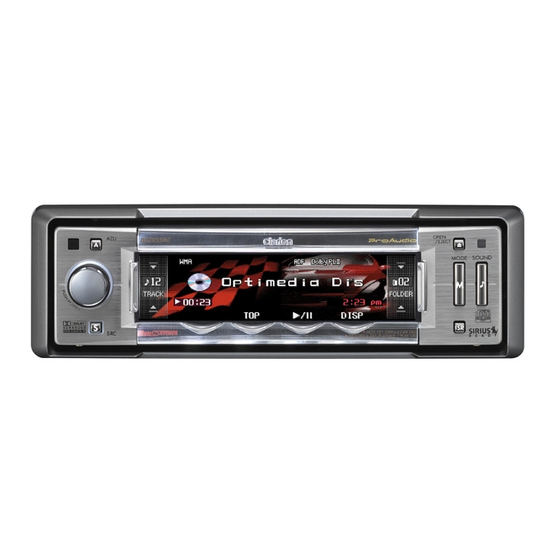
Clarion DXZ955MC Service Manual
Cd/mp3/wma receiver
cenet & touch panel control
music catcher
Hide thumbs
Also See for DXZ955MC:
- Owner's manual (58 pages) ,
- Installation/wire connection manual (2 pages)
Table of Contents
Advertisement
Quick Links
(DXZ955MC)
SPECIFICATIONS
FM tuner section
Frequency range:
Usable sensitivity:
50dB quieting sensitivity: 15dBf
Alternate channel selectivity:
Stereo separation:
Frequency response:
AM tuner section
Frequency range:
Usable sensitivity:
CD player section
System:
Usable discs:
Frequency response:
S/N ratio:
Dynamic range:
Distortion:
MP3/WMA mode
MP3 sampling rate:
MP3 bit rate:
WMA bit rate:
Logical format:
Audio section
Maximum power output: 53Wx4
Continous average power output:
Line output level:
Bass control action:
Treble control action:
Clarion Co., Ltd.
50 Kamitoda, Toda-shi, Saitama 335-8511 Japan
Service Dept.: 5-66 Azuma , Kitamoto-shi, Saitama 364-0007 Japan
Tel: +81-48-541-2335 / 2432 FAX: +81-48-541-2703
87.9MHz to 107.9MHz(PE-2747B-A)
87.0MHz to 108.0MHz(PE-2747K-A)
9dBf
70dB
32dB (1kHz)
30Hz to 15kHz (+3/-3dB)
530kHz to 1710kHz(PE-2747B-A)
531kHz to 1629kHz(PE-2747K-A)
25uV
Compact disc digital audio system
Compact disc
5Hz to 20kHz (+1/-1dB)
100dB (1kHz)
96dB (1kHz)
0.005%
11.025kHz to 48kHz
8kbps to 320kbps/VBR
48kbps to 192kbps
ISO9660 level1,2
JOLIET or Romeo
18Wx4, into 4ohm, 20Hz to 20kHz,
1%THD
4V/F 2ch+4V/R 2ch (CD 1kHz)
4V/SUB WOOFER 2ch (CD 1kHz)
+12/-12dB(50Hz)
+12/-12dB (12.5kHz)
Service Manual
CD/MP3/WMA Receiver
CeNET & Touch Panel Control
Music Catcher
Model
(PE-2747B-A / For U.S.A.)
Model
(PE-2747K-A / For other countries)
Music Catcher mode
HQ:
LP:
General
Power supply voltage:
Current consumption:
Speaker impedance:
Dimensions(mm):
Source unit;
Remote control unit;
Weight:
Source unit;
Remote control unit;
NOTES
* Use only compact discs bearing the
* Some CDs recorded in CD-R/CD-RW mode may not be
usable.
*
marks, or registerd trademarks of Microsoft Corporation
in the United States and/or other countries.
* This product includes technology owned by Microsoft Cor-
poration and cannot be used or distributed without a li-
cense from MSLGP.
* This product is manufactured under license from Dolby
Laboratories."Dolby","Pro Logic" and the double-D sym-
bol are trademarks of Dolby Laboratories.
* We cannot supply PWB with component parts in principle.
When a circuit on PWB has failure, please repair it by
component parts base. Parts which are not mentioned in
service manual are not supplied.
* Specifications and design are subject to change without
notice for further improvement.
- 1 -
Published by Service Dept.
298-6229-00 Mar.2005 X
Printed in Japan
Approximately 266 minutes,66tracks
(4 minutes for each)
Approximately 354 minutes,88tracks
(4 minutes for each)
14.4V DC(10.8V to 15.6V allow-
able) negative ground
Less than 15A,3A
4ohm(4ohm to 8ohm allowable)
178(W)x50(H)x160(D)
44(W)x113(H)x13(D)
1.7kg
40g(including battery)
or
, and the Windows
logo are trade-
DXZ955MC
DXZ956MC
mark.
Advertisement
Table of Contents

Related Manuals for Clarion DXZ955MC


Summary of Contents for Clarion DXZ955MC
-
Page 1: Specifications
Clarion Co., Ltd. Published by Service Dept. 50 Kamitoda, Toda-shi, Saitama 335-8511 Japan 298-6229-00 Mar.2005 X Service Dept.: 5-66 Azuma , Kitamoto-shi, Saitama 364-0007 Japan Printed in Japan Tel: +81-48-541-2335 / 2432 FAX: +81-48-541-2703 Service Manual CD/MP3/WMA Receiver CeNET & Touch Panel Control... - Page 2 345-3799-20 Disconnect the battery terminal after turning the ignition *B-A: For DXZ955MC (PE-2747B-A) key off. If wrong wiring connections are made with the battery connected, a short circuit and/or fire may occur. If extensive damage is caused due to negligence of repair, CAUTIONS the legal responsibility shall be with the repairing company.
-
Page 3: System Check
Input 1000kHz/60dBu and measure with CW, the adjustment value is written in EEP-ROM IC. (adjustable tolerance +1/-1 KHz) 4. AM S-meter adjust Input 1000kHz/70dBu/40dBu and measure with modulation (1KHz/30%), the calculated offset value and inclination are written in EEP-ROM IC. (adjustable tolerance +3/-3 KHz) DXZ955MC DXZ956MC - 3 -... - Page 4 Also when there is big flicker, it returns to No.1 and it readjusts. (D figure) (E figure) Right and left dot part Right and left 5. If there is no problem, the hole for the adjustment of the rear cover of DCP is closed with the film (347-7745-00). Closed hole DXZ955MC DXZ956MC...
-
Page 5: Error Displays
If an error display other than the ones described above appears, turn off the power, then press the [ RELEASE ] button and remove the DCP. And press the reset button for about 2 seconds with a thin rod. DXZ955MC DXZ956MC - 5 -... - Page 6 : O : The start signal output terminal for the source driver. pin 34: LBR : O : The output terminal of signal that controls the horizontal reversing display. pin 35: SPL : O : The starting signal output to the source driver. DXZ955MC DXZ956MC - 6 -...
- Page 7 97: DSP 2 INI RST : O : The initial reset signal output to DSP-2. pin 45: OSD CD 2 :I/O: The parallel data input/output for the on pin 98: NU : IN : Not in use. screen display. DXZ955MC DXZ956MC - 7 -...
- Page 8 : IN : Touch panel co-ordinates input. pin 38: Y G IN : IN : Touch panel co-ordinates input. pin 39: X G IN : IN : Touch panel co-ordinates input. pin 40: Vref : - : Reference voltage. DXZ955MC DXZ956MC - 8 -...
- Page 9 : - : Not in use. pin 74 : PUR2 : IN : For flash memory. pin 75 : NMI : IN : Connect to VDD. pin 48: NU : - : Not in use. DXZ955MC DXZ956MC - 9 -...
-
Page 10: Block Diagram
: I/O : Address / Data bus. pin 87 : Address/Data 3 : I/O : Address / Data bus. pin 88 : Address/Data 4 : I/O : Address / Data bus. BLOCK DIAGRAM CD mechanism section:929-0601-81 DXZ955MC DXZ956MC - 10 -... - Page 11 Main section CONVERTOR TOUCH PANEL DXZ955MC DXZ956MC - 11 -...
-
Page 12: Exploded View Parts List
816-3005-50 FLAT WIRE(TO LCD PWB) 1-56 347-7624-00 DOUBLE FACE 1-25 060-4011-80 PHOTO-TR 1-57 ------------- SWITCH PWB 1-26 347-7557-00 SHADE 1-58 060-4017-90 IR-RECIEVER 1-27 716-0872-01 PAD SCREW(M1.7x6) 1-59 013-6302-50 SWITCH 1-28 716-0872-12 PAD SCREW(M1.7x8) 1-60 001-7040-91 DIODE DXZ955MC DXZ956MC - 12-... - Page 13 738-1722-17 PRECISION SCREW(1.7x2.2) 335-7399-00 HOOK(L) 347-6275-00 FILM 750-6787-00 SPRING(L) 341-1817-00 ROLLER 331-3942-00 LEVER-UP(R) 946-0079-01 GEAR BOX ASSY 331-3938-00 LEVER-LO(R) 345-5560-00 CUSHION 331-3939-00 LEVER-UP(L) 947-0513-02 T-LIM GEAR ASSY 331-3940-00 LEVER-LO(L) 345-5558-00 CUSHION 716-1758-00 PAD SCREW(pin2x5) 345-5559-00 CUSHION DXZ955MC DXZ956MC - 13-...
- Page 14 305-0337-00 SIDE-CVR(R) 313-1923-00 HEAT SINK 307-0708-00 REAR-CVR 331-3953-00 FAN HOLDER 331-3954-00 IC-HOLDER 331-3955-00 SHIELD CASE(F) 313-1924-00 HEAT SINK 286-6604-00 SETPLATE(PE-2747-BA) 076-6003-18 PLUG(18P) 286-6629-00 SETPLATE(PE-2747-KA) 001-7048-91 DIODE 347-7578-01 INSULATOR 092-2215-50 ANT-RECEPT 347-7579-00 INSULATOR 335-3700-00 MINI-SADDLE 020-3050-00 DC-MOTOR DXZ955MC DXZ956MC - 14-...
- Page 15 620-1023-23 CLAMPER PLATE 621-0616-20 POWER GEAR A 620-1721-20 SENSOR ARM 621-0617-20 POWER GEAR B 621-0708-20 CLAMPER RING 621-0618-20 POWER GEAR C 621-0626-21 STOPPER LINK 621-0619-20 POWER GEAR D 621-0627-21 DISC STOPPER 621-0620-20 THREAD GEAR A 750-3471-20 SENSOR SPRING DXZ955MC DXZ956MC - 15-...
- Page 16 CD mechanism section:929-0601-81 H4 H5 DXZ955MC DXZ956MC - 16-...
-
Page 17: Electrical Parts List
168-1022-55 1000pF K C 529 043-0540-00 6.3V 10uF C 219 163-1073-35 16V 100uF C 357 166-1811-50 180pF CH C 530 043-0540-00 6.3V 10uF C 220 163-2263-55 35V 22uF C 358 043-0551-90 6.3V 4.7uF M C 531 043-0540-00 6.3V 10uF DXZ955MC DXZ956MC -17-... - Page 18 C 650 168-1032-55 0.01uF K IC 603 051-5408-08 S-80921CNMC 125-3004-90 KTA1504S C 651 168-1042-78 16V 0.1uF IC 604 051-3406-90 NJM2078M Q 101 125-4012-90 KTD1304 C 652 043-0552-90 6.3V 47uF M IC 605 051-5440-08 S-80931CNMC Q 102 125-4012-90 KTD1304 DXZ955MC DXZ956MC -18-...
- Page 19 119-0000-05 1/10W 0 ohm JW R 264 119-1031-15 1/10W 10k ohm R 404 119-0000-05 1/10W 0 ohm JW R 108 119-4721-15 1/10W 4.7k ohm R 265 119-1021-15 1/10W 1k ohm R 405 119-0000-05 1/10W 0 ohm JW DXZ955MC DXZ956MC -19-...
- Page 20 043-0542-00 25V 4.7uF 001-0367-91 1SS226 C 707 C 717 D 704 168-1032-55 0.01pF 043-0542-00 25V 4.7uF 001-0367-91 1SS226 C 708 C 718 D 705 C 709 168-1032-55 0.01pF C 719 043-0541-00 6.3V 22uF D 706 001-7040-91 NSCW100 DXZ955MC DXZ956MC -20-...
- Page 21 001-7078-90 NSCW505T R 817 032-0140-50 1/10W 10k ohm F R 888 119-4791-15 1/10W 4.7 ohm D 803 001-7078-90 NSCW505T R 821 119-1001-15 1/10W 10 ohm 039-2679-00 PWB(WITHOUT D 804 001-7078-90 NSCW505T R 822 119-1001-15 1/10W 10 ohm COMPONENT) DXZ955MC DXZ956MC -21-...
- Page 22 R 296 119-4731-15 1/16W 47k ohm 039-2681-00 PWB(WITHOUT R 291 119-4731-15 1/16W 47k ohm R 297 119-1011-15 1/16W 100 ohm COMPONENT) INNER ES FPC(B7) section REF No. PART No. DESCRIPTION J 1000 074-1278-01 SOCKET(16P) J 1001 074-1278-01 SOCKET(16P) DXZ955MC DXZ956MC -22-...
- Page 23 LED PWB (B9) section: 929-0601-81 REF No. PART No. DESCRIPTION REF No. PART No. DESCRIPTION REF No. PART No. DESCRIPTION 001-7058-90 AN1105W-RR 060-4015-90 PS1192H 013-7413-50 LIMIT 001-7058-90 AN1105W-RR 060-4015-90 PS1192H 039-1944-21 PWB (WITHOUT 074-1138-60 10P 013-7414-50 CHUCKING COMPONENT) DXZ955MC DXZ956MC -23-...
-
Page 24: Printed Wiring Board
FLAT WIRE 816-3005-50 SOLDER SIDE COMPONENT SIDE Caution: COMPONENT SIDE: Parts on the component side seen from the component side are indicated. SOLDER SIDE: Parts on the solder side seen from the solder side are indicated. DXZ955MC DXZ956MC - 24 -... - Page 25 SOLDER SIDE: Parts on the solder side seen from the solder side are indicated. COMPONENT SIDE SOLDER SIDE VIDEO PWB (B4) To J604 of Main PWB(B1) page 29 DXZ955MC DXZ956MC - 25 -...
- Page 26 COMPONENT SIDE SOLDER SIDE Slot PWB (B6) To J4 of CD PWB(B8) page 28 1 2 3 4 5 6 7 8 FLAT WIRE 816-2639-00 EXTENSION LEAD 854-4581-50 To J801 of Main PWB(B1) page 29 DXZ955MC DXZ956MC - 26 -...
-
Page 27: Circuit Diagram
CIRCUIT DIAGRAM 1/12 DD PWB(B5) section Slot PWB(B6) section DD PWB (B5) To J202 of Main PWB(B1) page 35 Slot PWB (B6) MEMORY CARD SLOT DXZ955MC DXZ956MC - 27 -... - Page 28 LED PWB-B(B9) Caution: SOLDER SIDE:Parts on the soider side seen from the solder side are indicated. Caution: COMPONENT SIDE:Part on the component side seen from the component side are indicated. SOLDER SIDE LED PWB-A(B9) SOLDER SIDE DXZ955MC DXZ956MC - 28 -...
- Page 29 INNER ES FPC(B7) J1000 To J703 of Switch PWB(B2) page 24 FLAT WIRE 816-2626-50 INNER ES FPC(B7) To J3 of CD PWB(B8) J1001 page 28 Inner escutcheon section MOTOR ASSY To J702 of Switch PWB(B2) page 24 DXZ955MC DXZ956MC - 29-...
- Page 30 PRINTED WIRING BOARD 6/6 Main PWB(B1) section 2/2 3 4 5 6 (PE2747BA) (PE2747KA) SOLDER SIDE Caution: SOLDER SIDE: Parts on the solder side seen from the solder side are indicated. DXZ955MC DXZ956MC - 30-...
- Page 31 BACK UP 14V To 3/6 page 33 To 2/6 page 32 To 4/6 page 33 To 6/6 page 35 To 5/6 page 34 To 2/6 page 32 (PE2747BA) (PE2747KA) To 6/6 page 35 To 5/6 page 34 DXZ955MC DXZ956MC - 31 -...
- Page 32 CIRCUIT DIAGRAM 3/12 Main PWB(B1) section 2/6 To 5/6 page 34 To 3/6 page 33 To 6/6 page 35 To 5/6 page 34 To 1/6 page 31 To 1/6 page 31 DXZ955MC DXZ956MC - 32 -...
- Page 33 CIRCUIT DIAGRAM 4/12 CIRCUIT DIAGRAM 5/12 Main PWB(B1) section 3/6 Main PWB(B1) section 4/6 To 2/6 page 32 To 1/6 page 31 To 6/6 page 35 To 6/6 page 35 To 1/6 page 31 DXZ955MC DXZ956MC - 33 -...
- Page 34 CIRCUIT DIAGRAM 6/12 Main PWB(B1) section 5/6 FRONT-R REAR-R REAR-L FRONT-L To 6/6 page 35 To 2/6 page 32 To 3/6 page 33 To 2/6 page 32 To 3/6 page 33 DXZ955MC DXZ956MC - 34 -...
- Page 35 CIRCUIT DIAGRAM 7/12 Main PWB(B1) section 6/6 To 4/6 page 33 To 2/6 page 32 To 3/6 page 33 To 5/6 page 34 INNER ESCUTCHEON section To 5/6 page 34 DXZ955MC DXZ956MC - 35 -...
- Page 36 5V usually 5V pulse when pulse when pulse when pulse when touching touching touching touching pulse output DIMMER ON: pulse in 1.4V or less AUTO-DIMMER ON in 2.4V or more DIMMER Off: 5.0V AUTO-DIMMER OFF DXZ955MC DXZ956MC - 36 -...
- Page 37 CIRCUIT DIAGRAM 9/12 LCD PWB(B3) section To J704 of Switch PWB(B2) page 36 it changes by the bright setting 2.3V to 3.4V it changes by the bright setting 4.7V to 6.8V PULSE DXZ955MC DXZ956MC - 37 -...
- Page 38 CIRCUIT DIAGRAM 10/12 VIDEO PWB(B4) section To J604 of Main PWB(B1) page 31 DXZ955MC DXZ956MC - 38 -...
- Page 39 CIRCUIT DIAGRAM 11/12 CD PWB (B8) section 1/2 LED PWB(B9) section CD MECHANISM CD PWB (B8) OTHER LED PWB-B(B9) OTHER LED PWB-A(B9) FLAT WIRE 816-2624-50 DXZ955MC DXZ956MC -39-...
-
Page 40: Circuit Diagram - Cd Mechanism
CIRCUIT DIAGRAM 12/12 CD PWB(B8) section 2/2 CD MECHANISM TO CD PWB(B8) 1/2 PAGE 39 D-OUT LRCK BCLK To CD PWB(B8) Page 39 DXZ955MC DXZ956MC -40-...
Need help?
Do you have a question about the DXZ955MC and is the answer not in the manual?
Questions and answers