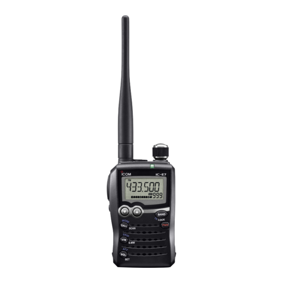
Icom IC-E7 Service Manual
Vhf/uhf dualband fm transceiver icom ic-e7
Hide thumbs
Also See for IC-E7:
- Instruction manual (96 pages) ,
- Service manual (6 pages) ,
- Instruction manual (12 pages)
Table of Contents
Advertisement
Quick Links
Download this manual
See also:
Instruction Manual
Advertisement
Table of Contents

Subscribe to Our Youtube Channel
Related Manuals for Icom IC-E7


Summary of Contents for Icom IC-E7
- Page 1 SERVICE MANUAL VHF/UHF DUALBAND FM TRANSCEIVER S-14217HZ-C1 Nov. 2005...
- Page 2 8. READ the instructions of test equipment thoroughly before connecting equipment to the transceiver. Icom, Icom Inc. and logo are registered trademarks of Icom Incorporated (Japan) in the United States, the United Kingdom, Germany, France, Spain, Russia and/or other countries.
-
Page 3: Table Of Contents
TABLE OF CONTENTS SECTION 1 SPECIFICATIONS SECTION 2 INSIDE VIEWS SECTION 3 DISASSEMBLY INSTRUCTIONS SECTION 4 CIRCUIT DESCRIPITON 4 - 1 RECEIVER CIRCUITS ............. . 4 - 1 4 - 2 TRANSMITTER CIRCUITS . -
Page 4: Specifications
25/30/50/100 and 200 kHz 148.000–179.995 –14 dBµ – : 50 Ω (SMA type) • Antenna impedance 330.000–369.995 +5 dBµ • Power supply requirement : Specifi ed Icom's battery 370.000–399.995 –10 dBµ pack only 400.000–429.995 –13 dBµ – (operating voltage 3.7 V) 430.000–449.995 –15 dBµ... -
Page 5: Main Unit
SECTION 2 INSIDE VIEWS • MAIN UNIT (TOP VIEW) (IC4: M30220FCRP) (IC4: M30220FCRP) (IC4: M30220FCRP) Reference Reference Reference frequency generator frequency generator frequency oscillator (X1: CR-813 7.325MHz) (X1: CR-813 7.325MHz) (X1: CR-813 7.325 MHz) PTT detector PTT detector PTT detector (Q14: 2SA1832) (Q14: 2SA1832) (Q14: 2SA1832) -
Page 6: Disassembly Instructions
SECTION 3 DISASSEMBLY INSTRUCTIONS • Removing the chassis • Removing the MAIN unit and PA board 1 Remove the battery pack. 1 Unscrew 2 screws A, then remove the LCD panel B. 2 Remove the jack cap A and unscrew the antenna nut B. 2 Unscrew 5 screws C and dial nut D. -
Page 7: Circuit Descripiton
SECTION 4 CIRCUIT DESCRIPTION 4-1 RECEIVE CIRCUITS • While receiving 500–999 MHz The 500–999 MHz band signals are passed through the HPF 4-1-1RF CIRCUITS (MAIN UNIT) (L41, C311, C313) and band switch (D54), then applied to This transceiver has 4 RF circuits to provide wide receiving the RF amplifier (Q45) via the attenuator (D46). - Page 8 4-1-3 2ND IF AND DEMODULATOR CIRCUITS The amplified AF signals are applied to the electric volume (IC7, pin 11) and level adjusted. The level adjusted AF signals (MAIN UNIT) are output from pin 12, and applied to the AF amplifi er (IC9, The 1st IF signal is converted into the 2nd IF signal and pin 2) to obtain more than 50 mW of AF output power.
-
Page 9: Transmitter Circuits
The amplified noise components are converted into the 4-2-2 MODULATION CIRCUIT (VCO BOARD) pulse-type signal at the noise detector section, and output The modulation circuit modulates the VCO oscillating signal from pin 13 as the “NOISE” signal. The “NOISE” signal is with the AF signals from the microphone and the tone applied to the CPU (IC4, pin 47). -
Page 10: Pll Circuits
4-3 PLL CIRCUITS If the receiving frequency is 500 MHz and above, the buffer- amplified signals are applied to the doubler circuit (Q18, 4-3-1 VCO CIRCUITS (VCO BOARD) D14, D15) via doubler switch (D12). The doubled signals are This transceiver has 3 VCOs; 50 MHz VCO, 144 MHz VCO then applied to the 1st mixer (IC16, pin 3) via doubler switch and 430 MHz VCO. -
Page 11: Port Allocations
4-4 PORT ALLOCATIONS Port Description 4-4-1 CPU (MAIN UNIT; IC4) Name Outputs VHF RF circuit control signal to the Port Description band selector (Q36). Name VHFC "High": While receiving on the VHF band Input port for [Y], [Z]keys. (76−300 MHz). Input port for [BAND], [CALL] and [V/M] keys. -
Page 12: Power Supply Circuits
4-4-1 CPU (MAIN UNIT; IC4)-continue 4-5 POWER SUPPLY CIRCUITS Port Line Description Description Name The same voltage as attached battery pack. Input port for [SQL] key (S7). Common 3 V converted from VCC line at the "Low": While [SQL] is pushed. CPU3 regulator (IC11). -
Page 13: Adjustment Procedures
SECTION 5 ADJUSTMENT PROCEDURES 5-1 PREPARATION When adjusting IC-E7, these test equipments and the JIG cable (see the illust below) are required. ¤ REQUIRED TEST EQUIPMENTS EQUIPMENT GRADE AND RANGE EQUIPMENT GRADE AND RANGE Measuring range : 0.1–3 W Frequency range : 0.1–1300 MHz Frequency range : 100–500 MHz... - Page 14 ¤ ENTERING ADJUSTMENT MODE ¤ KEY ASSIGNMENTS FOR ADJUSTMENT MODE q Turn the power OFF. w Connect the JIG cable (see page 5-1) to the [MIC/SP] jack. e Turn the "S1" of the JIG cable ON. r While pushing [FUNC], [BAND] and [Y] key, turn the power ON.
-
Page 15: Freqency And Transmit Adjustment
5-2 FREQUENCY AND TRANSMIT ADJUSTMENT • Set the specifi ed value using [DIAL], and push [BAND] to store the set value. Then push [CALL] to move to the next adjustment item. NOTE: "REFERENCE FREQUENCY" should be adjusted before "DEVIATION" and "RX SENSITIVITY," and "DEVIATION" should be adjusted before "DTCS BALANCE"... - Page 16 5-3 SIGNALING AND RECEIVE ADJUSTMENT • Set the specifi ed value using [DIAL], and push [BAND] to store the set value. Then, push [CALL] to move to the next adjustment item. NOTE: "DTCS BALANCE" should be adjusted before "CTCSS DEVIATION," and "RX SENSITIVITY" should be adjusted before "FM/WFM S-METER"...
-
Page 17: Receive Adjustment
• RECEIVE ADJUSTMENT (continued) ADJUSTMENT ITEM ADJUSTMENT CONDITION VALUE [t44] 13 • Set the SSG as; Frequency : Specifi ed frequency* • Receiving Push [FUNC]+[BAND] (Automatic adjustment) [t54] 14 • Set the SSG as; Frequency : Specifi ed frequency* • Receiving [t64] 15 •... -
Page 18: Main Unit
SECTION 6 PARTS LIST • IC-E7 [MAIN UNIT] [MAIN UNIT] ORDER ORDER DESCRIPTION DESCRIPTION LOCATION LOCATION 1130012690 S.IC HN58X24256FPIE (SOP8) 11.5/61.9 1750001070 S.DIO DAN235ETL 37.2/41.9 1750001070 S.DIO DAN235ETL 16.1/22.3 1110006720 S.IC R3112N291A-TR-F 9.3/46.2 1790001621 S.DIO 1SV308 22/40 1140013010 S.IC M30220FCRP 27/53.5... - Page 19 [MAIN UNIT] [MAIN UNIT] ORDER ORDER DESCRIPTION DESCRIPTION LOCATION LOCATION 7030005050 S.RES ERJ2GEJ 103 X (10 kΩ) 14.6/57.7 6200006981 S.COL ELJRE R10GFA 10.8/43.9 R101 7030005120 S.RES ERJ2GEJ 102 X (1 kΩ) 24.8/52.7 L101 6200003640 S.COL MLF1608E 100K-T 9.3/53.1 R104 7030005030 S.RES ERJ2GEJ 152 X (1.5 kΩ) 37.2/17 L102 6200004480 S.COL MLF1608D R82K-T...
- Page 20 [MAIN UNIT] [MAIN UNIT] ORDER ORDER DESCRIPTION DESCRIPTION LOCATION LOCATION R236 7030007290 S.RES ERJ2GEJ 222 X (2.2 kΩ) 28.7/43.5 R358 7030005050 S.RES ERJ2GEJ 103 X (10 kΩ) 30.5/18 R237 7030005240 S.RES ERJ2GEJ 473 X (47 kΩ) 12.8/25.1 R359 7030005040 S.RES ERJ2GEJ 472 X (4.7 kΩ) 30.8/19.3 R238 7030005240 S.RES ERJ2GEJ 473 X (47 kΩ)
- Page 21 [MAIN UNIT] [MAIN UNIT] ORDER ORDER DESCRIPTION DESCRIPTION LOCATION LOCATION 4030016930 S.CER ECJ0EB1A104K 22.4/16.8 C186 4030016790 S.CER ECJ0EB1C103K 35.1/43.5 4030017040 S.CER ECJ0EB1A333K 8/64.7 C187 4030017380 S.CER ECJ0EC1H050B 35.9/40.5 4030016930 S.CER ECJ0EB1A104K 20.7/5.4 C189 4030017460 S.CER ECJ0EB1E102K 23.3/38.5 4030017460 S.CER ECJ0EB1E102K 26.4/9.5 C190 4550007600 S.TAN F920J106MPABMA...
- Page 22 [MAIN UNIT] [MAIN UNIT] ORDER ORDER DESCRIPTION DESCRIPTION LOCATION LOCATION 5040002930 S.LED SML-512MW T86 6.7/23.2 C288 4030017460 S.CER ECJ0EB1E102K 15.5/46.7 5040002930 S.LED SML-512MW T86 7/12 C289 4030017420 S.CER ECJ0EC1H470J 2.9/62.9 5040003160 S.LED BRPY1211C-TR 26.7/72.7 C290 4030017510 S.CER ECJ0EC1H680J 20/59.2 C291 4550007080 S.TAN TEESVA 1C 106M8R 37/61.4 C292...
-
Page 23: Pa Board
[VCO BOARD] [VCO BOARD] ORDER ORDER DESCRIPTION DESCRIPTION LOCATION LOCATION 4030017460 S.CER ECJ0EB1E102K 22.3/8.6 7030007300 S.RES ERJ2GEJ 332 X (3.3 kΩ) 13.7/17.3 4030017460 S.CER ECJ0EB1E102K 17.2/4 7030009290 S.RES ERJ2GEJ 562 X (5.6 kΩ) 10/11.3 4030017460 S.CER ECJ0EB1E102K 20.2/1.1 7030009290 S.RES ERJ2GEJ 562 X (5.6 kΩ) 7.5/7 4030017610 S.CER ECJ0EC1H090C 21/10.6... - Page 24 [MAIN UNIT] [PA BOARD] ORDER ORDER DESCRIPTION DESCRIPTION LOCATION LOCATION 7030003440 S.RES ERJ3GEYJ 102 V (1 kΩ) 24.5/40.9 2260002060 S.SW SKQGAD 6/11.9 7030003500 S.RES ERJ3GEYJ 332 V (3.3 kΩ) 40.3/35.4 2260002060 S.SW SKQGAD 6/27.5 7030003560 S.RES ERJ3GEYJ 103 V (10 kΩ) 41.1/37.3 7030003320 S.RES ERJ3GEYJ 101 V (100 Ω) 40.3/32.8...
- Page 25 SECTION 7 MECHANICAL PARTS AND DISASSEMBLY [CHASISS PARTS] [MAIN UNIT] REF. ORDER REF. ORDER DESCRIPTION QTY. DESCRIPTION QTY. 6510025010 Antenna connector SMA-R2869 7600000210 Encoder TP70N00E2015F-1903 2510000840 Speaker CS028014-12 6450001910 SP/MIC jack HSJ1594-010150 8900010960 Cable OPC-1129 5030002860 LCD A01B004X 8010020240 2869 chassis 7700002310 Microphone EM-140 8210022691...
- Page 26 MP1 (P) J4 (M) MP28 (C) MP20 (C) 52.44 (2 MP13 (C) 29.9 (1 S8 (M) MP29 (C) MP14 (C) MC1 (M) PA board MP29 (C) EP2 (M) DS1 (M) MP1 (V) MP33 (C) VCO board 28.2 (1 46.83 (1 MP5 (C) MP27 (C) Unit: mm (inch)
- Page 27 SECTION 8 SEMICONDUCTOR INFORMATION • TRANSISTORS AND FET'S • DIODES 2SA1576 S 2SA1588 GR 2SA1832 GR 2SC4213 B 2SC4617 S 1SS400 1SV286 1SV308 DA221 DAN222 (Symbol: A) (Symbol: T7) (Symbol: TX) (Symbol: K) (Symbol: N) (Symbol: FS) (Symbol: ZG) (Symbol: SG) (Symbol: AB) (Symbol: BR) 2SC5006...
- Page 28 9-4 BC-164 SECTION 9 BOARD LAYOUTS • TOP VIEW 9-1 MAIN UNIT to PA board • TOP VIEW to CHASSIS J1 to CHASSIS 9-3 VCO BOARD • TOP VIEW 9-2 PA BOARD • TOP VIEW 9 - 1...
- Page 29 • BOTTOM VIEW (BC-164) • BOTTOM VIEW (MAIN UNIT) • BOTTOM VIEW (VCO BOARD) • BOTTOM VIEW (PA BOARD) DBL1 DBL2 VSHIFT to VCO board J1 VSHIFT DBL2 DBL1 to MAIN unit J6 to MAIN unit 9 - 2...
- Page 30 SECTION 10 BLOCK DIAGRAM VCO BOARD PA BOARD Q2:2SC5998 Q44:UNR9213J +10V Q8,Q11:2SC5006 D12:1SV308 Q18:2SC5508 D16:1SV308 D2:MA6S121 D34:1SV308 D41:1SV308 D5:1SV286 D14,D15:MA2S077 D17:1SV308 D1:HVC132 UHF_Tx(400-479) MHz Q19:2SC5108 D13:1SV308 D18:DAN235E D37:1SV308 D45:1SV308 D9:1SV308 LEVEL LOOP TX/RX DRIVE BUFF DOUBLER DRIVE CHANGE 430M Q3:RQA003 Q56:2SC4617 Q14:2SC5108 Q1:2SC5006...
- Page 31 SECTION 11 CIRCUIT DIAGRAM MAIN UNIT (1) BUS LINE1 R2 10k A01B004X 2SA1576 UNR9215J XP1113 R170 C549 0.15 0.001 CPU3V C103 C503 R4 68k 0.033 0.001 UNR9211J 2SC4617 R183 470 R184 470 C104 IC17 LMV321IDCK UNR9213J PSET SEG16 SEG18/P102 P15/KI5 SEG15 800C SEG17/P101...
- Page 32 MAIN UNIT (2) BUS LINE1 C220 C255 C302 C310 1SV308 0.001 17.5n CP13 D43 DAN235E C226 L20 0.22µ C267 C281 CHASSIS 0.15µ 0.12µ R262 C515 C199 UNR9213J R220 10k 1SV308 C242 47p XP1113 DAN235E C221 2SC5006 C294 IC16 µPC2757TB C238 C256 0.68µ...
- Page 33 SECTION 12 BC-164 [CHASSIS PARTS] [ACCESSORIES] REF. ORDER REF. ORDER DESCRIPTION QTY. DESCRIPTION QTY. 8010020220 2878 case Optional product AC adaptor BC-145LE/LUK POWER 8110008590 2878 cover RSQ035P03TR 2SC4081 8930067800 2878 lens 100µ R74 0 CHARGE 8930067810 2878 lock plate to MAIN unit SM240A-T 8930067830 2878 springe...
- Page 34 Phone : +34 (93) 590 26 70 Fax : +34 (93) 589 04 46 Glenwood Centre #150-6165 : http://www.icomspain.com Highway 17 Delta, B.C., V4K 5B8, Canada E-mail : icom@icomspain.com Phone : +1 (604) 952-4266 Fax : +1 (604) 952-0090 : http://www.icomcanada.com E-mail : info@icomcanada.com Unit 9, Sea St., Herne Bay, Kent, CT6 8LD, U.K.
- Page 35 S-14217HZ-C1 1-1-32, Kamiminami, Hirano-ku, Osaka 547-0003, Japan © 2005 Icom Inc.
Need help?
Do you have a question about the IC-E7 and is the answer not in the manual?
Questions and answers