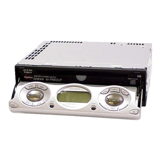
Sony CDX-M850MP Service Manual
Fm/mw/lw compact disc player
Hide thumbs
Also See for CDX-M850MP:
- Operating instruction (178 pages) ,
- Operating instructions manual (96 pages) ,
- Service manual (60 pages)
Table of Contents
Advertisement
Quick Links
SERVICE MANUAL
Ver 1.0 2003. 04
• The tuner and CD sections have no adjustments.
SPECIFICATIONS
AUDIO POWER SPECIFICATIONS (US MODEL)
POWER OUTPUT AND TOTAL HARMONIC DISTORTION
23.2 watts per channel minimum continuous average power into
4 ohms, 4 channels driven from 20 Hz to 20 kHz with no more
than 5% total harmonic distortion.
CD player section
Signal-to-noise ratio
90 dB
Frequency response
10 – 20,000 Hz
Wow and flutter
Below measurable limit
Tuner section
FM
Tuning range
87.5 – 107.9 MHz (US, Canadian model)
87.5 – 108.0 MHz (AEP, UK, E model)
Antenna terminal
External antenna connector
Intermediate frequency 10.7 MHz/450 kHz
Usable sensitivity
9 dBf
Selectivity
75 dB at 400 kHz
Signal-to-noise ratio
67 dB (stereo),
69 dB (mono)
Harmonic distortion at 1 kHz
0.5% (stereo),
0.3% (mono)
Separation
35 dB at 1 kHz
Frequency response
30 – 15,000 Hz
AM (US, Canadian model)
Tuning range
530 – 1,710 kHz
Antenna terminal
External antenna connector
Intermediate frequency 10.7 MHz/450 kHz
Sensitivity
30 µV
Sony Corporation
9-877-224-01
2003D0400-1
e Vehicle Company
© 2003. 04
Published by Sony Engineering Corporation
CDX-M850MP
Model Name Using Similar Mechanism
CD Drive Mechanism Type
Optical Pick-up Name
MW/LW (AEP, UK, E model)
Tuning range
Aerial terminal
Intermediate frequency 10.7 MHz/450 kHz
Sensitivity
Power amplifier section
Outputs
Speaker impedance
Maximum power output 52 W × 4 (at 4 ohms)
General
Outputs
FM/AM COMPACT DISC PLAYER
FM/MW/LW COMPACT DISC PLAYER
US Model
Canadian Model
AEP Model
UK Model
E Model
CDX-MP40
MG-393MC-121//K
KSS-721A
MW: 531 – 1,602 kHz
LW: 153 – 279 kHz
External aerial connector
MW: 30 µV
LW: 40 µV
Speaker outputs (sure seal connectors)
4 – 8 ohms
Audio outputs (front/rear)
Subwoofer output (mono)
Power antenna relay
control terminal (US, Canadian model)
Power aerial relay
control terminal (AEP, UK, E model)
Power amplifier control
terminal
– Continued on next page –
US, Canadian Model
AEP, UK, E Model
1
Advertisement
Table of Contents

Related Manuals for Sony CDX-M850MP


Summary of Contents for Sony CDX-M850MP
- Page 1 External antenna connector Intermediate frequency 10.7 MHz/450 kHz FM/AM COMPACT DISC PLAYER Sensitivity 30 µV US, Canadian Model FM/MW/LW COMPACT DISC PLAYER AEP, UK, E Model Sony Corporation 9-877-224-01 2003D0400-1 e Vehicle Company © 2003. 04 Published by Sony Engineering Corporation...
-
Page 2: Service Notes
LES COMPOSANTS IDENTIFIÉS PAR UNE MARQUE 0 SUR LES DIAGRAMMES SCHÉMATIQUES ET LA LISTE DES PIÈCES SONT CRITIQUES POUR LA SÉCURITÉ DE FONCTIONNEMENT. NE REMPLACER CES COMPOSANTS QUE PAR DES PIÈCES SONY DONT LES NUMÉROS SONT DONNÉS DANS CE MANUEL OU DANS LES SUPPLÉMENTS PUBLIÉS PAR SONY. - Page 3 CDX-M850MP AEP, UK, E model: Notes on CD-Rs (recordable CDs)/CD-RWs (rewritable CDs) This unit can play the following discs: Type of discs Label on the disc Audio CD This label is located on the bottom of the chassis. MP3 files This label is located on the drive unit’s internal chassis.
- Page 4 CDX-M850MP EXTENSION CABLE AND SERVICE POSITION When repairing or servicing this set, connect the jig (extension cable) as shown below. • Connect the MAIN board (CNP301) and the SERVO board (CN1) with the extension cable (Part No. J-2502-062-1). MAIN BOARD CNP301...
-
Page 5: Table Of Contents
CDX-M850MP TABLE OF CONTENTS 1. GENERAL Location of Controls ..............6 Connection example (US, Canadian Model) ......6 Connections (US, Canadian Model) ........7 2. DISASSEMBLY 2-1. Front Panel Assy ..............8 2-2. CD Mechanism Block, Front Panel Assy ......9 2-3. -
Page 6: General
*1 When an optional MD unit is connected. t EQ7 button b Main display window g SEEK/AMS (</,) buttons *2 Available only when an optional Sony portable u SOUND button c IMAGE button 23 device is connected to AUX IN terminal of the unit. -
Page 7: Connections (Us, Canadian Model)
CDX-M850MP Connections (US, Canadian Model) Source selector (not supplied) Sélecteur de source Supplied with the CD/MD changer (non fourni) Fourni avec le changeur de CD/MD Selector de fuente Suministrado con el cambiador de CD/MD (no suministrado) XA-C30 BUS AUDIO IN... -
Page 8: Disassembly
CDX-M850MP SECTION 2 DISASSEMBLY Note : This set can be disassemble according to the following sequence. 2-7. CHASSIS (T) SUB ASSY 2-1. FRONT PANEL ASSY (Page 11) (Page 8) 2-8. LEVER SECTION 2-9. SERVO BOARD 2-2. CD MECHANISM BLOCK, (Page 12) -
Page 9: Cd Mechanism Block, Front Panel Assy
CDX-M850MP 2-2. CD MECHANISM BLOCK, FRONT PANEL ASSY 7 bracket (CD) 5 CD mechanism block 6 PTT 2.6x6 8 tension spring (flexible) 0 cover (flexible) 9 slider (flexible) 3 PTT 2.6x4 qa CNP909 slider (flexible) flexible board Note: When installing the flexible board, 2 PTT 2.6x4... -
Page 10: Motor Block Assy, Cam (R) Assy
CDX-M850MP 2-4. MOTOR BLOCK ASSY, CAM (R) ASSY Note : Install the motor block assy and cam (R) assy in this roder. For phase alignment between cams (L) and (R), see page 15 and 17. 1 PTT 2.6x6 Note: Install the cam (R) assy with 4 PTT 2.6x6... -
Page 11: Heat Sink
CDX-M850MP 2-6. HEAT SINK 5 heat sink 4 PTT 2.6x6 3 PTT 2.6x12 1 PTT 2.6x6 2 PTT 2.6x6 2-7. CHASSIS (T) SUB ASSY 2 P 2x3 3 P 2x3 4 chassis (T) sub assy 1 Unsoldering three lead wires. -
Page 12: Lever Section
CDX-M850MP 2-8. LEVER SECTION 5 guide (disc) 6 lever (R) 3 tension spring (LR) 7 lever (L) 1 special screw 2 DISC IN SW board 4 two claws 2-9. SERVO BOARD 9 SERVO board 8 special screw 7 special screws 3 Removal the solders. -
Page 13: Shaft Roller Assy, Load Sw Board
CDX-M850MP 2-10. SHAFT ROLLER ASSY, LOAD SW BOARD • When installing, take note of the positions arm (roller) and washers. (Fig. 1) 3 retaining ring (RA) shaft retainer (roller) shaft retainer (roller) 4 shaft retainer (roller) washer washer retaining ring (RA) arm Fig. -
Page 14: Optical Pick-Up Block
CDX-M850MP 2-12. OPTICAL PICK-UP BLOCK 3 P 2x3 1 P 2x3 7 PICK-UP FLEXIBLE board 4 plate spring (feed) 2 sled motor assy (M902) 5 optical pick-up (KSS-721A) 6 shaft (feed) assy... -
Page 15: Phase Alignment
CDX-M850MP SECTION 3 PHASE ALIGNMENT 3-1. ARM (A-L) ASSY, ARM (B-L) ASSY 3 arm (A-L) assy 4 type-E stop ring 1.5 2 type-E stop ring 1.5 1 arm (B-L) assy bracket (L) assy 3-2. CAM (L) 1 Move the arm (B-L) assy in the direction of the arrow A and the arm (A-L) assy in the direction of 3 type-E stop ring 1.5... -
Page 16: Motor Block
CDX-M850MP 3-3. MOTOR BLOCK 1 Turn the cam (L) and position the cam so that part A does not touch the SW board SW900. 3 PTT 2.6x6 4 PTT 2.6x6 2 motor block SWITCH board 5 PTT 2.6x6 SW900 cam (L) 3-4. -
Page 17: Arm (A-R) Assy, Arm (B-R) Assy
CDX-M850MP 3-5. ARM (A-R) ASSY, ARM (B-R) ASSY 4 type-E stop ring 1.5 3 arm (A-R) assy 2 type-E stop ring 1.5 1 arm (B-R) assy bracket (R) assy 3-6. CAM (R) 3 type-E stop ring 1.5 1 Move the arm (B-R) assy in the direction of the arrow A and the arm (A-R) assy in the direction of the arrow B fully (full open state). -
Page 18: Diagrams
CDX-M850MP SECTION 4 DIAGRAMS 4-1. IC PIN DESCRIPTIONS • IC3 HD6432238RWN35TEI (CD MASTER CONTROL) (SERVO Board (2/2)) Pin No. Pin Name Pin Description TEST Test mode selection pin Not used. (Open) DECXRST Reset signal output to the DSP IC “L”: reset DECSTBY Standby mode control signal output to the DSP IC “H”: standby... - Page 19 LED clock output for the jig LEDLAT LED latch signal output for the jig 89, 90 Not used. (Open) BUSON Sony-Bus BUS ON signal input from the bus interface BUCHK Back up power supply detection signal input A-ATT Audio muting control signal output CDON Power control signal output for the CD servo “H”: servo on, “L”: during loading...
- Page 20 CDX-M850MP • IC5 CXD9684R-005 (DSP) (SERVO Board (1/2)) Pin No. Pin Name Pin Description /RESET Reset input pin “L”: reset MIMD Microcomputer interface mode selection input “H”: I2C, “L”: TSB 3, 4 AD0, AD1 External SRAM address signal output MIDIO (I2C_SDA)
- Page 21 Electronic volume mute signal output I2C CKO Tuner/E-volume BUS clock output I2C SIO Tuner/E-volume BUS data output UNI SO SONY BUS data output UNI SI SONY BUS data input UNI CKO SONY BUS clock output TUNER ATT Tuner attenuate signal output...
- Page 22 CDX-M850MP Pin No. Pin Name Pin Description CD LM EJ CD eject motor control signal output Not used. (Open) CD RST CD servo reset signal output CD AO CD servo command/parameter discri. output Not used. (Open) CD STB CD servo data strobe signal output Not used.
- Page 23 CDX-M850MP • IC2 M30833FJGP-073 (DISPLAY SYSTEM CONTROL) (DISPLAY Board) Pin No. Pin Name Pin Description SYS CE Main chip enable input Not used. (Open) FL DAT3 FL serial data output Not used. (Open) FL CLK IN FL serial clock input...
-
Page 24: Block Diagram -Cd Section
CDX-M850MP 4-2. BLOCK DIAGRAM — CD SECTION — RF AMP,DIGITAL SERVO OPTICAL PICK-UP DIGITAL SIGNAL PROCESSOR KSS-721A (Page 25) TUNER SECTION LOUT ROUT CD MASTER CONTROL CONV R-CH DEMOD 5V 3.3V PACK 38 PACK TSTB 34 TSTB DSUB CODE TSCK PROCESS CONV. -
Page 25: Block Diagram -Tuner Section
CDX-M850MP 4-3. BLOCK DIAGRAM — TUNER SECTION — PJ401 –1 BUS AUDIO ELECTRONIC VOLUME –2 Q408 IC401 R-CH AF BUFFER IC407 SECTION 4 PDL –5 OUT LF 42 MDL AUDIO OUT –6 32 AC OUT L FRONT (Page 24) Q171... -
Page 26: Block Diagram -Display Section
CDX-M850MP 4-4. BLOCK DIAGRAM — DISPLAY SECTION — BUFFER IC701 BUS ON BUS CLK SECTION BUS SI SYS RST (Page 24) BU CHK INVERTER BUS SO BUS INTERFACE SYSTEM CONTROL Q904 IC301 IC303 (2/2) CNP102 (BUS CONTROL IN) UNI SI... -
Page 27: Circuit Boards Location
CDX-M850MP 4-5. CIRCUIT BOARDS LOCATION THIS NOTE IS COMMON FOR PRINTED WIRING BOARDS AND SCHEMATIC DIAGRAMS. (In addition to this, the necessary note is printed in each block.) DISC IN SW board for schematic diagram: LIMIT SW board • All capacitors are in µF unless otherwise noted. pF: µµF... -
Page 28: Printed Wiring Boards -Cd Mechanism Section
CDX-M850MP 4-6. PRINTED WIRING BOARDS — CD MECHANISM SECTION — • Refer to page 27 for Circuit Boards Location. • Semiconductor Location Ref. No. Location (IC6) (IC12) (Q1) ): SIDE B R114 R121 R105 R107 IC12 R130 JR14... - Page 29 CDX-M850MP R118 R111 R109 R100 R117 (Page 33) R148 R102 R128 R124 C113 R136 R132 R153 R131 JR15 R143 R145 R144 JR12 R142 R146...
-
Page 30: Schematic Diagram -Cd Mechanism Section (1/2)
CDX-M850MP • Refer to page 27 for Waveforms. 4-7. SCHEMATIC DIAGRAM — CD MECHANISM SECTION (1/2) — • Refer to page 40 for IC Block Diagram. Note: • Voltage is dc with respect to ground under no-signal conditions. no mark : CD PLAY M902 ∗... -
Page 31: Schematic Diagram -Cd Mechanism Section (2/2)
CDX-M850MP • Refer to page 27 for Waveform. 4-8. SCHEMATIC DIAGRAM — CD MECHANISM SECTION (2/2) — • Refer to page 40 for IC Block Diagrams. (Page 30) R105 (Page 30) C114 TP92 IC B/D TP31 TP33 R109 R111 TP30... -
Page 32: Printed Wiring Boards -Main Section
CDX-M850MP 4-9. PRINTED WIRING BOARDS — MAIN SECTION — • Refer to page 27 for Circuit Boards Location. • Semiconductor Location Ref. No. Location Ref. No. Location (D101) E-10 (D905) F-10 D906 (D102) E-10 (D103) E-10 (D907) (D104) E-11 D909... - Page 33 CDX-M850MP PJ401 CNJ101 CNP102 CNP101 C205 FB101 F101 FB102 IC201 CN503 TUX501 CN904 C101 R408 R442 R441 R443 CN903 R440 R103 D106 C442 C503 C505 L101 C506 C226 BATT AEP,UK model C507 L503 R402 R504 C502 R202 Q501 C102 R111...
-
Page 34: Schematic Diagram -Main Section (1/2)
CDX-M850MP • Refer to page 27 for Waveform. 4-10. SCHEMATIC DIAGRAM — MAIN SECTION (1/2) — • Refer to page 40 for IC Block Diagrams. C278 R440 R444 C206 C178 C207 R439 R443 C288 PJ401 R442 R446 C242 C188 C212... -
Page 35: Schematic Diagram -Main Section (2/2)
CDX-M850MP • Refer to page 27 for Waveform. 4-11. SCHEMATIC DIAGRAM — MAIN SECTION (2/2) — • Refer to page 40 for IC Block Diagrams. (Page 34) IC B/D Q904 IC301 D920 Q101 D104 CNP102 TH100 C303 L301 (Page C307... -
Page 36: Printed Wiring Board -Sub Section
CDX-M850MP 4-12. PRINTED WIRING BOARD — SUB SECTION — • Refer to page 27 for Circuit Boards Location. C535 C536 SW501 C537 R538 R509 C540 D506 C539 D511 IC503 D507 C538 Q504 R536 FB503 Q503 D512 R533 R531 R537 (Page 33) •... -
Page 37: Schematic Diagram -Sub Section
CDX-M850MP 4-13. SCHEMATIC DIAGRAM — SUB SECTION — • Refer to page 41 for IC Block Diagrams. CN502 Q503 R532 R525 R534 R531 R533 Q504 D512 SW501 D513 D514 C536 (Page 35) R536 R537 R538 CN501 C537 R509 C533 C540... -
Page 38: Printed Wiring Board -Display Section
CDX-M850MP 4-14. PRINTED WIRING BOARD — DISPLAY SECTION — • Refer to page 27 for Circuit Boards Location. R971 C905 LED909 LED931 FL900 R999 FMA12 R988 S909 C962 R994 R989 FMA10 FB914 R981 C912 S931 D901 FB913 FB912 C914 R967... -
Page 39: Schematic Diagram -Display Section
CDX-M850MP • Refer to page 27 for Waveform. 4-15. SCHEMATIC DIAGRAM — DISPLAY SECTION — • Refer to page 41 for IC Block Diagrams. R946 R936 R950 R952 R945 R954 R951 R956 R953 R958 R955 R960 R957 R961 R959 R962... -
Page 40: Ic Block Diagrams
CDX-M850MP 4-16. IC BLOCK DIAGRAMS IC1 µPD63711GC-8EU (SERVO Board (1/2)) IC2 BA5810FP (SERVO Board (2/2)) IC12 TC7SH08FU (SERVO Board (2/2)) 71 70 BIAS IN B IN A LOADING PRE MICROCOMPUTER INTERFACE OPIN4+ FWD REV AGCI 50 C2D3 – OPIN4– COMPARATOR... - Page 41 CDX-M850MP IC201 TDA8588J/N1 (MAIN Board (1/2)) IC407 LA2901V-TLM (MAIN Board (1/2)) SIGNAL LFIN- LFOUT LFIN+ I2C BUS VREF SIGNAL LRIN- LROUT LRIN+ PGND3 LGND VREF LIFT IN_RL LIFT IN_FL LIFT SGND LOUT PROTECTION DIAGNOSTIC IN_FR IN_RR VREF ACGND VCCL VCCR...
- Page 42 CDX-M850MP IC401 TDA7416 (MAIN Board (1/2)) 30 29 24 23 HIGH PASS MIXER FILTER2 SOFT STEP FADER ACOUTR SOFT STEP ACINSW FADER ACOUTSW HIGH PASS MIXER 22 OUTRF FILTER WOOFER SOFT STEP OUTRR FILTER FADER 7 BAND EQUALIXER 20 AC2INR...
-
Page 43: Exploded Views
CDX-M850MP SECTION 5 EXPLODED VIEWS NOTE: • The mechanical parts with no reference The components identified by • Color Indication of Appearance Parts mark 0 or dotted line with mark number in the exploded views are not supplied. Example : 0 are critical for safety. -
Page 44: Cam Section
CDX-M850MP 5-2. CAM SECTION M601 Ref. No. Part No. Description Remark Ref. No. Part No. Description Remark 3-230-495-01 CAM (L) 3-230-494-01 GEAR (C) X-3380-549-1 ARM (B-R) ASSY 3-230-496-01 CAM (R) X-3380-544-2 BRACKET (L) ASSY X-3380-545-2 BRACKET (R) ASSY X-3380-548-1 ARM (B-L) ASSY... -
Page 45: Main Board Section
CDX-M850MP 5-3. MAIN BOARD SECTION supplied not supplied TUX501 F901 not supplied not supplied Ref. No. Part No. Description Remark Ref. No. Part No. Description Remark 3-230-493-01 GEAR (DRIVE SHAFT) 1-777-246-41 CORD (WITH CONNECTOR) (ANTENNA) 3-230-444-01 GUIDE (DRIVE SHAFT) 1-790-375-32 CORD (WITH CONNECTOR) (SUB OUT (MONO)) -
Page 46: Front Panel Section
CDX-M850MP 5-4. FRONT PANEL SECTION not supplied FL900 LCD2 not supplied Ref. No. Part No. Description Remark Ref. No. Part No. Description Remark X-3383-766-1 PANEL (KEY) ASSY (S), FRONT (US,CND) 3-248-789-01 BUTTON (RESET-DSPL) X-3383-768-1 PANEL (KEY) ASSY (S), FRONT (AEP,UK,E) -
Page 47: Cd Mechanism Section (1)
CDX-M850MP 5-5. CD MECHANISM SECTION (1) (MG-393MC-121//K) M903 Ref. No. Part No. Description Remark Ref. No. Part No. Description Remark A-3274-253-A DISC IN SW BOARD, COMPLETE 3-221-779-02 BRACKET (MOTOR) 3-040-039-03 CHASSIS (T) 3-040-034-01 SPRING (RA), TENSION 3-040-038-01 SPRING (LR), TENSION... -
Page 48: Cd Mechanism Section (2)
CDX-M850MP 5-6. CD MECHANISM SECTION (2) (MG-393MC-121//K) not supplied Ref. No. Part No. Description Remark Ref. No. Part No. Description Remark 3-040-025-02 ARM, CHUCKING 3-040-033-01 SPRING (KF1), TENSION 3-040-031-01 DAMPER (T) A-3307-422-A CHASSIS (M) COMPLETE ASSY 3-040-056-01 LEVER (D) 3-040-059-01 SPRING (TR), TENSION... -
Page 49: Cd Mechanism Section (3)
CDX-M850MP 5-7. CD MECHANISM SECTION (3) (MG-393MC-121//K) not supplied M902 The components identified by Les composants identifiés par une mark 0 or dotted line with mark marque 0 sont critiques pour 0 are critical for safety. la sécurité. Replace only with part number Ne les remplacer que par une piéce... -
Page 50: Electrical Parts List
CDX-M850MP SECTION 6 DISC IN SW DISPLAY ELECTRICAL PARTS LIST NOTE: • Due to standardization, replacements in • Items marked “*” are not stocked since The components identified by mark 0 or dotted line with mark the parts list may be different from the they are seldom required for routine service. - Page 51 CDX-M850MP DISPLAY Ref. No. Part No. Description Remark Ref. No. Part No. Description Remark FB926 1-500-329-21 INDUCTOR, FERRITE BEAD R914 1-218-867-11 RES-CHIP 6.8K 1/16W FB971 1-500-329-21 INDUCTOR, FERRITE BEAD R915 1-218-863-11 RES-CHIP 4.7K 1/16W R916 1-218-859-11 RES-CHIP 3.3K 1/16W < FLUORESCENT INDICATOR >...
- Page 52 CDX-M850MP DISPLAY LIMIT SW LOAD SW MAIN Ref. No. Part No. Description Remark Ref. No. Part No. Description Remark R990 1-216-025-11 RES-CHIP 1/10W A-3274-933-A MAIN BOARD, COMPLETE (US,CND) (US,CND) A-3274-934-A MAIN BOARD, COMPLETE (AEP,UK,E) R991 1-218-855-11 RES-CHIP 2.2K 1/16W *********************...
- Page 53 CDX-M850MP MAIN Ref. No. Part No. Description Remark Ref. No. Part No. Description Remark C311 1-128-647-11 DOUBLE LAYERS 0.1F 5.5V C503 1-124-259-11 ELECT 4.7uF C312 1-124-584-00 ELECT 100uF (AEP,UK,E) C313 1-164-156-11 CERAMIC CHIP 0.1uF C505 1-162-964-11 CERAMIC CHIP 0.001uF C315...
- Page 54 CDX-M850MP MAIN Ref. No. Part No. Description Remark Ref. No. Part No. Description Remark < JACK > D909 8-719-988-61 DIODE 1SS355TE-17 D920 8-719-988-61 DIODE 1SS355TE-17 CNJ101 1-764-270-21 JACK, STEREO MINIATURE (DIA.3.5) D921 8-719-988-61 DIODE 1SS355TE-17 (REMOTE IN) < FERRITE BEAD >...
- Page 55 CDX-M850MP MAIN Ref. No. Part No. Description Remark Ref. No. Part No. Description Remark Q380 1-801-806-11 TRANSISTOR DTC144EKA (AEP,UK,E) R324 1-216-845-11 METAL CHIP 100K 1/10W Q401 8-729-900-53 TRANSISTOR DTC114EK R325 1-216-845-11 METAL CHIP 100K 1/10W Q402 8-729-027-23 TRANSISTOR DTA114EKA-T146 R326...
- Page 56 CDX-M850MP MAIN SERVO Ref. No. Part No. Description Remark Ref. No. Part No. Description Remark R427 1-216-864-11 METAL CHIP 1/10W R922 1-216-845-11 METAL CHIP 100K 1/10W R429 1-202-926-11 METAL CHIP 1/10W R929 1-216-837-11 METAL CHIP 1/10W R430 1-218-725-11 METAL CHIP...
- Page 57 CDX-M850MP SERVO Ref. No. Part No. Description Remark Ref. No. Part No. Description Remark 1-162-970-11 CERAMIC CHIP 0.01uF JR17 1-216-864-11 METAL CHIP 1/10W 1-107-826-11 CERAMIC CHIP 0.1uF JR21 1-216-864-11 METAL CHIP 1/10W 1-107-826-11 CERAMIC CHIP 0.1uF 1-107-826-11 CERAMIC CHIP 0.1uF <...
- Page 58 CDX-M850MP SERVO SWITCH Ref. No. Part No. Description Remark Ref. No. Part No. Description Remark 1-216-845-11 METAL CHIP 100K 1/10W < VIBRATOR > 1-216-845-11 METAL CHIP 100K 1/10W 1-216-845-11 METAL CHIP 100K 1/10W 1-795-520-11 VIBRATOR, CERAMIC (16.9344MHz) 1-216-845-11 METAL CHIP...
- Page 59 CDX-M850MP Ref. No. Part No. Description Remark Ref. No. Part No. Description Remark MISCELLANEOUS PARTS FOR INSTALLATION AND CONNECTIONS *************** *************************************** 1-776-207-72 CORD (WITH CONNECTOR) (POWER) X-3382-647-1 FRAME ASSY, FITTING (US,CND,E) X-3366-405-1 SCREW ASSY (EXP), FITTING (AEP,UK,E) 1-776-527-71 CORD (WITH CONNECTOR) (ISO) (POWER)
- Page 60 CDX-M850MP REVISION HISTORY Clicking the version allows you to jump to the revised page. Also, clicking the version at the upper on the revised page allows you to jump to the next revised page. Ver. Date Description of Revision 2003. 04...
Need help?
Do you have a question about the CDX-M850MP and is the answer not in the manual?
Questions and answers