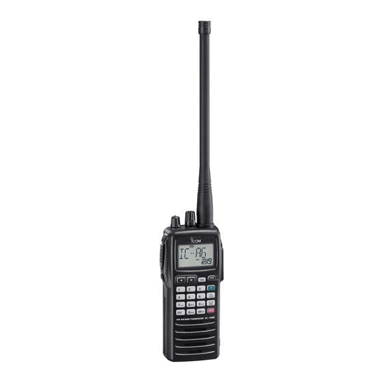
Icom IC-A24 Service Manual
Vhf air band transcever
Hide thumbs
Also See for IC-A24:
- Instruction manual (44 pages) ,
- Service manual (12 pages) ,
- Operation manual (2 pages)

Related Manuals for Icom IC-A24


Summary of Contents for Icom IC-A24
- Page 1 VHF AIR BAND TRANSCEVER iC-a24 iC-a24e iC-a6 iC-a6e S-14115HZ-C1-q July. 2007...
- Page 2 8. READ the instructions of test equipment throughly before connecting a test equipment to the transceiver. Icom, Icom Inc. and logo are registered trademarks of Icom Incorporated (Japan) in the United States, the United Kingdom, Germany, France, Spain, Russia and/or other countries.
-
Page 3: Table Of Contents
TABLE OF CONTENTS SECTION 1 SPECIFICATIONS SECTION 2 INSIDE VIEWS SECTION 4 CIRCUIT DESCRIPTION 4 - 1 RECEIVER CIRCUITS ............. . .4 - 1 4 - 2 TRANSMITTER CIRCUITS . -
Page 4: Specifications
: 20 channels × 10 banks • Number of memory channels • Power supply requirement : Specifi ed ICOM's battery packs (BP-208N, BP-209N, BP-210N, BP-211N) • External power supply requirement : 11.0 V DC • Current drain (at 7.2 V DC) : Transmit 1.5 A typical... -
Page 5: Logic Unit
INSIDE VIEWS • LOGIC UNIT • LOGIC UNIT LED DRIVE LED drivers VOR circuit VOR circuit (Q8, Q9: UNR9213J) (Q8, Q9: UNR9213J×2) (IC-A24 only) (IC-A24/A24E only) (IC1: μPD78F0338GC-9EB) (IC1: μPD78F0338GC-9EB) LED DRIVE LED drivers Q1: 2SB1132 Q1: 2SB1132 RESET IC... - Page 6 SECTION 3 DISASSEMBLY INSTRUCTION 2 Unsolder 1 point H. • REMOVING THE CHASSIS PANEL 3 Unscrew 2 nuts I. 1 Remove the Jack cap A. 4 Unscrew 3 screws J and remove the LOGIC unit from 2 Remove [VOL] knob B and [DIAL] knob C. 3 Unscrew the ANT nut D.
-
Page 7: Receiver Circuits
SECTION 4 CIRCUIT DESCRIPTION 4-1 RECEIVER CIRCUITS The signals from the RF circuit are mixed at the 1st mixer 4-1-1 ANTENNA SWITCHING CIRCUIT (RF UNIT) (Q12) with a 1st LO signal (AM; 77.95–106.925 MHz, The antenna switching circuit functions as a low-pass filter FM;... - Page 8 (2) FM DETECTOR CIRCUIT The CPU analyzes the noise condition and outputs the con- The amplified signal is applied to the limiter amplifier section trol signal to the expander IC (IC5). The expander IC (IC5, of the IF IC (IC1, pin 5) and is then applied to the quadra- pin 4) outputs the squelch control signal as the “AFC”...
- Page 9 IC5, pin 7 as a “OFF FLAG” signal (VORD). 4-1-9 VOR NAVIGATION CIRCUIT (LOGIC UNIT) (IC-A24/E ONLY) From the AF signal, the VOR circuit detects a variable signal (VORC) and reference signal (VORS) from a VOR station. The VOR circuit sends these signals to the CPU (IC1).
-
Page 10: Rf Unit
4-2-3 DRIVE/POWER AMPLIFIER CIRCUITS 4-2 TRANSMITTER CIRCUITS (RF UNIT) 4-2-1 MICROPHONE AMPLIFIER CIRCUIT (RF UNIT) The drive amplifier circuit amplifies the transmit signal to The microphone amplifier circuit amplifies audio signals with a level needed for the power amplifier circuit. The power +6 dB/octave pre-emphasis characteristics from the micro- amplifier circuit amplifies this to obtain a specified transmit phone to a level needed for the modulation circuit. -
Page 11: Pll Circuit
4-3 PLL CIRCUITS (RF UNIT) 4-4 POWER SUPPLY CIRCUITS A PLL circuit provides stable oscillation of the transmit VOLTAGE LINES (MAIN UNIT) frequency and receive 1st LO frequency. The PLL output LINE DESCRIPTION compares the phase of the divided VCO frequency to the The voltage from the connected DC power reference frequency. -
Page 12: Port Allocations
4-5 PORT ALLOCATIONS 4-5-2 EXPANDER (RF unit; IC5) 4-5-1 CPU (LOGIC unit; IC1) Port Description number name Port Description number name Outputs control signal to the AF out controller (Q35, Q36) for AF amplifi er Outputs control signal for the 5 V PCON (IC6). - Page 13 Capacity : More than 1 W ■ ■ SYSTEM REQUIREMENT ENTERING ADJUSTMENT MODE • RS-232C serial port or USB port 1. Turn transceiver’s power off. Connect IC-A24/A6 and PC ® ® • Microsoft Windows 98/SE/ME/2000/XP with the optional OPC-478/U/UC. 2. Right click the CS-24's icon on the desktop and select the ■...
- Page 14 DC POWER DC POWER SUPPLY DC ammeter SUPPLY DC ammeter [DC 11V] 7.2 V/5 A 11 V/5 A IC-A24/E IC-A6/E Battery type detector Battery type detector • DISPLAY IN THE ADJUSTMENT MODE Operating frequency Adjustment item Adjustment value 5 - 2...
- Page 15 5-2 ADJUSTMENT ADJUSTMENT ADJUSTMENT CONDITION OPERATION • Measure the current at "00" point ( A ). IDLING 1 • Operating frequency: 127.500 MHz CURRENT • Connect a DC ammeter between the battery terminal and • Rotate [DIAL] to adjust the current A +500 mA.
-
Page 16: Adjustment Procedures
5-2 ADJUSTMENT (continued) ADJUSTMENT ADJUSTMENT CONDITION OPERATION MAX. 4 • Operating frequency: 127.500 MHz • Rotate [DIAL] to set to 30% modulation. MODULATION • Connect an 11 V power supply to the [DC 11V] jack. (PRESET) • Transmitting 5 • Operating frequency: 118.025 MHz •... -
Page 17: Soft Wear Adjustment
• Receiving 5 • Operating frequency: 163.275 MHz • Push [ENT] key. • Receiving SQUELCH 1 • Operating frequency: 108.025 MHz (IC-A24) • Push [ENT] key. 118.025 MHz (IC-A6) • Connect an SSG to the antenna connector and set as: Level : –111 dBm* (0.63 µV) for IC-A24... - Page 18 ADJUSTMENT ADJUSTMENT CONDITION OPERATION VOR OFF • Operating frequency: 108.000 MHz • Push [ENT] key. (IC-A24 only) • Connect a VOR tester to the antenna connector and set Level : –90 dBm* (7.1 µV) Modulation : 9960 Hz, 10% 30 Hz, 30% Bearing : 0°...
-
Page 19: Logic Unit
DESCRIPTION DESCRIPTION LOCATION LOCATION 1140012401 S.IC uPD780338GC-503-9EB-A 45.1/18.7 7030005290 S.RES ERJ2GEJ 682 X (6.8 k) 1110006310 S.IC BD5245G-TR 53.8/4.4 [IC-A24/E] only 15.9/21.9 1110006090 S.IC XC6202P502PR 76.2/6.3 7030005100 S.RES ERJ2GEJ 154 X (150 k) 1130012430 S.IC S-24CS64A0I-T8T1G 57.4/6.2 [IC-A24/E] only 13.8/20.1 IC11 1110003790 S.IC... - Page 20 4030017430 S.CER ECJ0EC1H101J 72.2/30.6 4030017460 S.CER ECJ0EB1E102K 15/38.7 C623 4030017430 S.CER ECJ0EC1H101J 73.9/33.9 4030017460 S.CER ECJ0EB1E102K 58.8/10.5 C101 4030017460 S.CER ECJ0EB1E102K [IC-A24/E] only 16.9/19.7 C102 4030017730 S.CER ECJ0EB1E471K [IC-A24/E] only 21.2/21.2 6510020120 S.CNR AXK6S40545P 68.8/38.4 C103 4550006250 S.TAN TEESVA 1A 106M8R [IC-A24/E] only 5.7/31.5...
-
Page 21: Rf Unit
1530002601 S.TR 2SC4215-O (TE85R,F) 92.6/6.7 6200012470 S.COL 0.30-1.7-7TL 45.3N 24.9/24.3 1530003281 S.TR 2SC4211-6-TL-E 96.2/8.6 6200003550 S.COL MLF1608A 4R7K-T 21.8/20.8 1590003390 S.TR UNR9215J-(TX) [IC-A24/E] only 101.2/2.5 6200007730 S.COL LQW2BHN39NJ03L 26.6/25.4 1590003250 S.TR UNR9115J-(TX) 66.1/24.4 6200008090 S.COL LQW2BHN68NJ03L 40.5/23.6 1590003270 S.TR UNR9210J-(TX) 101.4/5.1 6200007760 S.COL LQW2BHN82NJ03L... - Page 22 [RF UNIT] [RF UNIT] ORDER ORDER DESCRIPTION DESCRIPTION LOCATION LOCATION 7030005210 S.RES ERJ2GEJ 822 X (8.2 k) 61.3/14.3 R193 7030010020 S.RES ERJ2RKF 154 X (150 k) 97.3/34 7030005050 S.RES ERJ2GEJ 103 X (10 k) 59.9/9.4 R194 7030010010 S.RES ERJ2RKF 334 X (330 k) 10.7/9.3 7030005570 S.RES ERJ2GEJ 820 X (82) 63.8/12.8...
- Page 23 [RF UNIT] [RF UNIT] ORDER ORDER DESCRIPTION DESCRIPTION LOCATION LOCATION R341 7030010040 S.RES ERJ2GEJ-JPW 88.3/21.4 4030017460 S.CER ECJ0EB1E102K 76.3/8.7 R342 7030011140 S.RES ERJ8GEYJ 0R00V 81.9/31.9 4550007200 S.TAN F930J476MBABMA R343 7030011140 S.RES ERJ8GEYJ 0R00V 81.5/21.9 except [AUS] 106/3.5 R344 7030003860 S.RES ERJ3GE JPW V 83.7/24.8 4550007620 S.TAN F931V224MAABMA...
- Page 24 [RF UNIT] [RF UNIT] ORDER ORDER DESCRIPTION DESCRIPTION LOCATION LOCATION C250 4550006250 S.TAN TEESVA 1A 106M8R 47.5/36.8 C387 4030018860 S.CER ECJ0EB0J105K 58.6/16.1 C251 4030016930 S.CER ECJ0EB1A104K 92.8/8.2 C390 4030017400 S.CER ECJ0EC1H220J 66.8/8.5 C253 4030016930 S.CER ECJ0EB1A104K 94.3/3.4 C391 4030017460 S.CER ECJ0EB1E102K 74.4/9.9 C254 4030016930 S.CER ECJ0EB1A104K...
- Page 25 SECTION 7 MECHANICAL PARTS [CHASSIS PARTS] [RF UNIT] ORDER ORDER DESCRIPTION QTY. DESCRIPTION QTY. 6450000870 HEC2711-01-020 6510022460 BNC-R162 6450001680 HSJ1122-010010 6510021901 BM02B-ASRS-TF (LF) (SN) 2510001092 036D0801B 6450001060 HSJ1493-01-010 6510024560 AXK5S40245P 8900009640 OPC-963 2260002840 SKHLLFA010 8210020970 2791 FRONT PANEL-1 (Incl. MP7, MP8, MP9, MP10) 2260002840 SKHLLFA010 [A24] 8210021211 2791 FRONT PANEL (B)-1...
- Page 26 MP3 (C) MP16 (C) MP19 (C) MP20 (C) MP37 (C) MP23 (C) J1 (C) MP4 (C) MP13 (C) MP1 (C) MP36 (C) MP22 (C) MP14 (C) MP12 (C) MP11 (C) MP2 (C) MP26 (C) MP33 (C) MP15 (C) MP38 (C) W1 (C) MP24 (C) SP1 (C)
- Page 27 SECTION 8 SEMICONDUCTOR INFORMATION • TRANSISTERS AND FETs • DIODES 2SA1586 GR 2SA1588 GR 2SB1132 T100 R 2SB1182 TL Q 2SB1201 S 1SS400 1SV246 1SV271 HVC350B HVU131TRF (Symbol: SG) (Symbol: ZG) (Symbol: BAR) (Symbol: None) (Symbol: B1201) (Symbol: A) (Symbol: CV) (Symbol: TG) (Symbol: B0) (Symbol: P1)
- Page 28 SECTION 9 BOARD LAYOUTS • LOGIC UNIT (TOP VIEW) 121.5 9 - 1...
- Page 29 • LOGIC UNIT (BOTTOM VIEW) LVIN UNLK DA2STB C615 DETO C162 R572 R589 C617 INTMIC R588 R570 C183 C169 EXTREGC SBATT R590 C182 C164 CHGVH JACKDET C165 CHGIH SDATA R567 R591 R571 C172 CHGC C166 CLONE C180 R145 DCIN R592 C171 C179 BEEP...
- Page 30 • RF UNIT (TOP VIEW) LVIN DA2STB UNLK DETO INTMIC SBATT EXTREGC JACKDET CHGVH SDATA CHGIH CHGC CLONE DCIN BEEP DA1STB PSTB CHASSIS INTPTT LIGHT RFDETV VORON VORDET RFSTB DCIN RSSI PDATA to LOGIC unit J1 C130 R147 C184 C287 R145 C186 C272...
- Page 31 • RF UNIT (BOTTOM VIEW) B-6285B C292 C418 C288 C239 R108 C289 R222 R349 C291 C274 C250 C263 R348 C273 C276 C284 C271 R139 R225 C244 C242 C283 C119 C270 C278 C282 C279 R342 C281 C280 EP10 R233 C420 R184 C262 C360 R189...
- Page 32 S-812C50BMC D10 MA2S111 INITIAL CPU5V RESET CURRENT VOLTAGE LINE MATRIX MATRIX COMMON LINE D1 MA2S111 D5 MA24111 [IC-A24/A6] only IC2 BD5245G IC3 XC6202P502PR D2 MA6S121 D6 MA2S111 [IC-A24/A24E] only DATA LINE RX LINE TX LINE 7.2V BATTERY PACK CHGC/CHGIH 10 - 1...
- Page 33 SECTION 11 VOLTAGE DIAGRAM A0280 • LOGIC UNIT C138 0.47 C139 0.47 RFDETV PDATA R SSI RSSI RFSTB VORDET C140 VORD 0.47 VORON LVIN SBATT PC K RFDETV DETO LIGHT R135 DCIN INTPTT 2.2M VOL_IN R592 R136 T:6.7 PSTB R578 DA1ST B 100K R137...
- Page 34 • RF UNIT IC16 C249 0.001 R338 SDATA D A1STB M62343GP EP16 MPZ2012S221A T:6.8 MPZ2012S221A R:0.0 2SB1132 R248 T:3.1 R:0.0 MA2S111 2SC4211 R322 R320 0.001 0.001 MA7 7 MA111 R332 XP4601 3.3K 0.001 220P 0.001 0.001 HVU131 T:3.5 R250 R:0.0 R219 C211 2SC4403...
- Page 35 Phone : +34 (93) 590 26 70 Fax : +34 (93) 589 04 46 Glenwood Centre #150-6165 : http://www.icomspain.com Highway 17 Delta, B.C., V4K 5B8, Canada E-mail : icom@icomspain.com Phone : +1 (604) 952-4266 Fax : +1 (604) 952-0090 : http://www.icomcanada.com E-mail : info@icomcanada.com Unit 9, Sea St., Herne Bay, Kent, CT6 8LD, U.K.
- Page 36 S-14115HZ-C1-q 1-1-32, Kamiminami, Hirano-ku, Osaka 547-0003, Japan © 2004–2007 Icom Inc.
Need help?
Do you have a question about the IC-A24 and is the answer not in the manual?
Questions and answers