Table of Contents
Advertisement
Quick Links
Colour Television
Contents
1
Technical Specifications, Connection Facilities,
2
3
Directions for Use
4
5
Faultfinding, and Repair Tips.
6
Block Diagram (Audio + Supply)
2
7
Electrical Diagrams and PWB lay-outs
AVI: Connections
AVI: HD-Matrix / Sync Remover (Diagram AV2) 45
AVI: Sync Processing
AVI: YPbPr-RGB Matrix
SSB: Tuner, IF, Sourse Select and Video
Processing
SSB: Input/Output
SSB: Audio Dolby
©
Copyright 2003 Philips Consumer Electronics B.V. Eindhoven, The Netherlands.
All rights reserved. No part of this publication may be reproduced, stored in a
retrieval system or transmitted, in any form or by any means, electronic,
mechanical, photocopying, or otherwise without the prior permission of Philips.
Published by WO 0364 Service PaCE
Page
2
6
7
26
29
37
38
39
40
41
42
43
Diagram PWB
(Diagram AV1) 44
52-54
46-48
(Diagram AV3) 46
46-48
(Diagram AV4) 47
46-48
(Diagram AV5) 48
46-48
(Diagram AV6) 49
46-48
(Diagram AV7) 50
46-48
(Diagram AV8) 51
46-48
(Diagram CF)
55
55
(Diagram FP1) 56
57
(Diagram K1)
58
65-70
(Diagram K2)
59
65-70
(Diagram K3)
60
65-70
(Diagram K4)
61
65-70
62
65-70
(Diagram K7)
63
65-70
Printed in the Netherlands
Contents
SSB: Source Sel. (add to K1)
Feature Box 7: Feature Box
SD Connector Panel
8
9
Subject to modification
Chassis
F21RE
AB
Page
(Diagram K8)
64
65-70
(Diagram L1)
71
74-75
72
74-75
73
74-75
(Diagram PS)
76
77-78
(Diagram SD)
79
80
81
87
99
101
107
114
EN 3122 785 13130
Advertisement
Table of Contents

Related Manuals for Philips F21RE


Summary of Contents for Philips F21RE
-
Page 1: Table Of Contents
All rights reserved. No part of this publication may be reproduced, stored in a retrieval system or transmitted, in any form or by any means, electronic, mechanical, photocopying, or otherwise without the prior permission of Philips. Published by WO 0364 Service PaCE... -
Page 2: And Chassis Overview
Technical Specifications, Connections, and Chassis Overview EN 2 F21RE AB 1. Technical Specifications, Connections, and Chassis Overview : 125 channels Technical Specifications Channel selections : Full cable, UVSH : 75 Ohm, IEC-type Aerial input 1.1.1 Reception 1.1.2 Miscellaneous : PLL... - Page 3 Technical Specifications, Connections, and Chassis Overview F21RE AB EN 3 Audio/Video - In EXT2: SCART - In/Out for VCR (RGB, CVBS, SVHS) 1 - Audio L 2.5 V_rms/33 kOhm 2 - Audio R 2.5 V_rms/33 kOhm 3 - Video CVBS 1 V_pp/75 Ohm...
- Page 4 Technical Specifications, Connections, and Chassis Overview EN 4 F21RE AB EXT4: SCART- In (CVBS, Audio) Audio Monitor - Out (Cinch: VGA2, RC-in) 1 - RC - in 2 - Audio L 0.5 V_rms/10 kOhm 3 - Audio R 0.5 V_rms/10 kOhm...
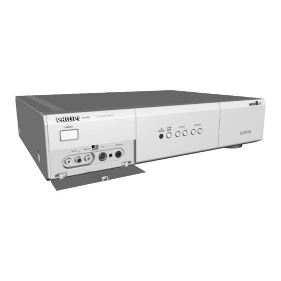
- Page 5 Technical Specifications, Connections, and Chassis Overview F21RE AB EN 5 Chassis Overview CL 26532054_008.eps 150502 Figure 1-8 Panel position 1. Front I/O Panel (FP). 2. Power Supply Panel (PS). 3. Double Window Panel (if present). 4. Feature Box (FBX). 5. Small Signal Panel (SSP).
-
Page 6: Safety Instructions, Maintenance, Warnings, And Notes
Safety Instructions, Warnings, and Notes EN 6 F21RE AB 2. Safety Instructions, Warnings, and Notes Safety Instructions stereo sound (L: 3 kHz, R: 1 kHz unless stated otherwise) and picture carrier at 61.25 MHz (NTSC). • Where necessary, measure the oscillograms and direct Safety regulations require that during a repair: voltages with (symbol ) and without (symbol ) aerial... -
Page 26: Mechanical Instructions
Mechanical instructions EN 26 F21RE AB 4. Mechanical instructions Index of this chapter: Service Positions and Panel Removal 1. Disassembly and Panel Overview 1. Top Cover Removal 4.2.1 Front I/O Panel 2. Panel Overview 2. Service Positions and Panel Removal 1. - Page 27 Mechanical instructions F21RE AB EN 27 4.2.2 4.2.4 Power Supply Panel Feature Box module FBX Module PS panel CL 16532098_016.eps 240901 Figure 4-5 Service position Power Supply (PS) 1. Remove the front panel, if it was not yet removed. 2. Remove the screws [1].
- Page 28 Mechanical instructions EN 28 F21RE AB 4.2.8 HD/SD (High/Standard Definition) Panel HD/SD panel CL 16532098_025.eps 180901 Figure 4-9 Removal of the bottom cover plate To access the copper side of the Small Signal Panel, it is CL 36532021_013.eps 270303 necessary to remove the metal bottom cover: 1.
-
Page 29: Service Modes, Error Codes
Service Modes, Error Codes, and Fault Finding F21RE AB EN 29 5. Service Modes, Error Codes, and Fault Finding Index of this section: 1. Test Points There is also the option of using ComPair, a hardware interface 2. Service Modes between a computer (see requirements) and the FTV chassis. - Page 30 Service Modes, Error Codes, and Fault Finding EN 30 F21RE AB 5.2.2 Service Alignment Mode (SAM) buffer that have not all been generated by a single module, there is probably another defect. In that situation, the message "Unknown" will then be displayed here. If there Purpose are no errors, "None"...
- Page 31 E-box. This information can be noisy picture may result if there is a bad antenna signal, or very helpful when talking with a dealer or Philips Customer the parameter of sharpness is set too high. Sharpness Care Centre (P3C).
- Page 32 Service Modes, Error Codes, and Fault Finding EN 32 F21RE AB – and CURSOR RIGHT keys on the remote control Off. – transmitter after pressing the "menu" button and navigating 4, 6, 8, 10, 12, 14, or 16 years. •...
- Page 33 5.4.1 Introduction 5.4.3 How to Connect ComPair ComPair (Computer Aided Repair) is a service tool for Philips 1. First, install the ComPair Browser software on your PC Consumer Electronics products. ComPair is a further (read the installation instructions carefully). development of the DST (special remote control transmitter for 2.
- Page 34 Service Modes, Error Codes, and Fault Finding EN 34 F21RE AB 7. Plug the mains adapter in an mains outlet and switch on the Table 5-2 Stepwise Shut-Down Table ComPair interface. The green and red LEDs light up together. The red LED turns off after approximately 1...
- Page 35 Service Modes, Error Codes, and Fault Finding F21RE AB EN 35 5.5.3 Error Codes If possible, check the entire contents of the error buffer. In some situations, an error code is only the result of another error code and not the actual cause of the problem (for example, a...
- Page 36 Without the accompanying plasma monitor, the Receiver box will go into Standby mode after a few seconds (this monitor detection is designed to prevent Philips Receiver boxes from being used with other brands of monitors). This detection can be overridden in the following way (to use, for example, a PC monitor): •...
-
Page 37: Block Diagrams
Block Diagrams, Testpoint Overviews and Waveforms F21RE AB 6. Block Diagrams, Testpoint Overviews and Waveforms Block Diagram (Video) CVBS-TXT-OUT 2D COMB R-TXT TUNER, IF, I/O, 7712 FEATURE BOX 7 7711 VIDEO CONTROL+ K2 CVBS-TER CVBS-TXT-OUT LATCH BLOCK FILTER 7555 PROM... - Page 38 Block Diagrams, Testpoint Overviews and Waveforms F21RE AB Block Diagram (Audio and Supply) AUDIO AUDIO SOURCE SELECTION +8V6 AUDIO TUNER + SOUND 1751 PROC. 7751 MSP3440 7777 SCART 1 TEA64220 2809 S BUS SIFM SOUND AUDIO CENTER IN IN-SC1-SNDR 3866...
-
Page 39: Powerlines Overview
Block Diagrams, Testpoint Overviews and Waveforms F21RE AB Powerlines Overview POWER SUPPLY STANDBY SUPPLY SUPPLY VIDEO + RC + SELECTION FRONT PANEL 3025 6025 3020 6203 6310 +5VSTB F072 5200 F067 RC. REC +8VF 3200 SB340 +5VSTBA 7710 +5VSTBY +5VSTBA... -
Page 40: I2C-Ic's Overview
Block Diagrams, Testpoint Overviews and Waveforms F21RE AB I2C-IC’s Overview TXT & CONTROL TUNER, IF, SOURCE SOUND PROC. VIDEO CONTROL & GEOMETRY SOURCE FEATURE BOX FALCONIC EAGLE +5V2 +5V2 SELECTION & VIDEO PROC. SELECTION 3036-C6 3036-B7 0361 0361 3033-C5 4402... -
Page 41: Testpoint Overviews (Av + Ps)
Block Diagrams, Testpoint Overviews and Waveforms F21RE AB Testpoint Overviews (AV + PS) 0309 AV interface panel (AV) Power supply panel (PS) F702 (COPPER TRACK SIDE) F703 0309 F706 F071 F709 F012 0341 0308 0309 COLD 0307 0307 0341 0328... -
Page 42: Testpoint Overviews (K + L + M)
Block Diagrams, Testpoint Overviews and Waveforms F21RE AB Testpoint Overviews (K + L + M) FBX panel (L) Small signal panel (K) T11 R/77-7003 F1K Y-OUT/19-7402 S3 SC/9-7300 S6 Frame/6-7300 S7 SS-Drive S8 EW/3-7300 C1 Reset/c-7007 0.2V / div DC 0.5V / div DC... -
Page 43: Wiring Diagram
Block Diagrams, Testpoint Overviews and Waveforms F21RE AB Wiring Diagram SMALL SIGNAL PANEL DIAGRAMS SS-panel TUNER K1 : 8 cable = from 1 to n 1020 cable = from 1 to 1 pos 8044 3 Fold 0328 0355 AUDIO_R TXDO... - Page 44 Circuit Diagrams and PWB Layouts F21RE AB 7. Circuit Diagrams and PWB Layouts AV Interface Panel AV INTERFACE PANEL +8VVA +8V6 +5VSTB +5VSTBA +5VSTBY Y_HD1 DIAGRAM CONNECTIONS R_SD G_SD +8VVA +8V6 +5VSTB +5VSTBA +5VSTBY B_SD Y_HD1 DIAGRAM +8VV +8V6 CVBS_Y_EXT3...
- Page 45 Circuit Diagrams and PWB Layouts F21RE AB HD Matrix + Sync Remover Panel (USA only) 2201 B1 F218 C6 2205 B1 F227 E6 2210 B1 F240 F6 2215 B4 F246 G2 HD-MATRIX+SYNC REMOVER (USA ONLY) 2216 F4 F250 H3 2227 F2...
- Page 46 Circuit Diagrams and PWB Layouts F21RE AB Sync Processing Panel (USA only) 1315 E10 7321-A E4 2302 B2 7321-B D4 2303 B4 7340-A G4 2304 B4 7340-B I2 2306 C2 7340-C G3 SYNC-PROCESSING (USA ONLY) 2307 B3 7341 I3 2308 B3...
-
Page 47: Avi: Vga / Hd-Selection
Circuit Diagrams and PWB Layouts F21RE AB VGA / HD Selection Panel 0301 F1 0370 A14 0371 G14 TO OUTPUT+SUPPLY 0398 B11 0399 B12 VGA/HD-SELECTION 2400 B2 2420 E10 2421 B6 2423 B6 2425 C6 2427 C6 TO 0370 USA ONLY... - Page 48 Circuit Diagrams and PWB Layouts F21RE AB Output Selection + Supply Panel 0303 B14 4521 E12 I543 F5 0306 H2 5513 H8 I544 F5 0307 G4 5520 D8 I545 E10 F521 F529 F560 F578 0310 G6 5523 A2 I546 E10...
- Page 49 Circuit Diagrams and PWB Layouts F21RE AB YPBPR RGB Matrix Panel 0300 G1 I622 D6 0304 B1 I623 D7 2601 A6 I626 B8 2607 A9 I627 C9 YPBPR-RGB-MATRIX 2608 B9 I631 C8 2610 A10 I635 C3 2622 D6 I636 D4...
-
Page 50: Avi: Output + Select. Supply
Circuit Diagrams and PWB Layouts F21RE AB Video + RC Selection Panel 0308 G6 F772 D13 0309 A1 F773 E13 0333 A14 I702 B3 0341 G14 I703 A4 0372 D14 I704 B3 VIDEO+RC-SELECTION TO AUDIO+CONTROL 2707 C4 I705 B4 2708 D5... -
Page 51: Avi: Audio + Control
Circuit Diagrams and PWB Layouts F21RE AB Audio + Control Panel 0302-A C1 F810 E2 0302-B D1 F811 F2 0302-C H1 F812 F2 0305 A1 F813 G2 0313-A E1 F814 H2 AUDIO+CONTROL 0313-B E1 F815 I2 0313-C I1 F816 D2... - Page 52 Circuit Diagrams and PWB Layouts F21RE AB Layout AV Panel (Top Side) 3122 123 60092 CL 26532118_009.eps 221002...
- Page 53 Circuit Diagrams and PWB Layouts F21RE AB Mapping Layout AV Mapping Top Side Mapping Bottom Side 0300 E2 2391 B2 2813 F3 3313 C1 3543 B3 3675 E2 3854 D4 6667 F1 7710 D2 F204 D3 F523 C1 F883 E3...
- Page 54 Circuit Diagrams and PWB Layouts F21RE AB Layout AV Panel (Bottom Side) 3122 123 60092 CL 26532118_010.eps 221002...
-
Page 55: Comb Filter Add-On
Circuit Diagrams and PWB Layouts F21RE AB 2D Comb Filter Add-on I01 B5 I03 B7 I05 C5 I07 C4 0002 C8 1001 A7 2001 D5 2003 B3 3001 C4 3003 D3 3999 E1 4001 D2 4003 D3 5001 D8 7001 C4... -
Page 56: Front Panel
Circuit Diagrams and PWB Layouts F21RE AB Front Panel 0301 F5 4061 D6 I145 B7 0302 E5 6001 B1 I146 B7 0303 D5 6002 B1 I147 C6 F098 3099 F099 3045 0304 B5 6012 F1 I148 C7 0305 A5 6025 D1... - Page 57 Circuit Diagrams and PWB Layouts F21RE AB Layout Front Panel Top Side 0301 B3 0302 B2 0303 B1 0304 B2 0305 B2 0308 A4 0309 A3 0344 A7 1006 A1 1008 B6 1010 B7 1012 B7 1014 B7 1016 B6...
- Page 58 Circuit Diagrams and PWB Layouts F21RE AB Small Signal Board: Tuner IF, Source Selection and Video Processing 0310 H2 1109 B6 2105 B5 2116 B1 2127 A4 2511 C13 2528 E15 2539 A7 2554 F11 2564 I14 2573 I13 3110 F4...
- Page 59 Circuit Diagrams and PWB Layouts F21RE AB Small Signal Board: Input/Output 0333 F7 2126 H8 2215 B7 2228 H2 3204 C2 3215 C4 3227 G12 3241 C11 3252 F8 3270 E11 4228 G6 6206 B4 6216 B7 6226 D10 6236 G2...
-
Page 60: Ssb: Sound Processing
Circuit Diagrams and PWB Layouts F21RE AB Small Signal Board: Sound Processing 0328 C14 3827 C11 0344 F14 3828 B11 0348 G14 3829 D11 SOUND PROCESSING K1:K8 1751 H7 3830 E12 2751 D3 3831 F12 2752 E3 3832 C8 A15 HP-R/3-0344... - Page 61 Circuit Diagrams and PWB Layouts F21RE AB Small Signal Board: Audio Dolby 2812 F4 2813 F7 F507 2814 F7 K3-12 SELECT_AUDIO_CINCH_1 F508 2815 E2 SELECT_AUDIO_CINCH_2 K3-13 +7V7 7772-A 2816 E2 100R 2839 K3-17 LM833DT I2S-DSP-OUT1 2817 F2 AUDIO DOLBY I504...
-
Page 62: Ssb: Video Control+ Geometry (Diagram K6)
Circuit Diagrams and PWB Layouts F21RE AB Small Signal Board: Video Control and Geometry 0311 G13 3407 B9 F647 C3 0315 D13 3408 B9 F648 C3 S3 SC/9-7300 S4 HFB/13-7300 S6 Frame/6-7300 S7 SS-Drive S8 EW/3-7300 0340 B11 3409 B9 F649 D3 VIDEO CONTROL &... -
Page 63: Ssb: Txt + Control
Circuit Diagrams and PWB Layouts F21RE AB Small Signal Board: TXT and Control 0341 B7 2005 B18 2013 K11 2025 K10 2035 L18 2044 K15 2054 I18 3004-B D10 3007 C10 3023-B L13 3027-D F10 3030-C K15 3034 J8 3042 L16... - Page 64 Circuit Diagrams and PWB Layouts F21RE AB Small Signal Board: Source Selection Add. to Diagram K1 0312 K3 0372 I17 2249 J4 2258 G8 2437 I16 2852 C6 2861 F6 2872 E5 3238 K4 3278 J9 3288 I5 3297 J8...
- Page 65 Circuit Diagrams and PWB Layouts F21RE AB Layout Small Signal Board (Overview Top Side) 2792 B3 3091 A2 3331 A5 3844 B3 4742 A5 0310 A4 2252 E5 6759 B2 3845 B3 4743 A4 0311 A5 2253 E5 2801 C1...
- Page 66 Circuit Diagrams and PWB Layouts F21RE AB Layout Small Signal Board (Part 1 Top Side) CL 36532030_01a.eps 020403...
- Page 67 Circuit Diagrams and PWB Layouts F21RE AB Layout Small Signal Board (Part 2 Top Side) CL 36532030_01b.eps 020403...
- Page 68 Circuit Diagrams and PWB Layouts F21RE AB Layout Small Signal Board (Overview Bottom Side) 0310 A2 2752 C4 3440 A1 5756 B5 0311 A1 2754 C5 3441 A1 5757 B2 0315 A1 2755 C4 3442 A2 5758 B5 0328 B3...
- Page 69 Circuit Diagrams and PWB Layouts F21RE AB Layout Small Signal Board (Part 1 Bottom Side) CL 36532030_02a.eps 020403...
- Page 70 Circuit Diagrams and PWB Layouts F21RE AB Layout Small Signal Board (Part 2 Bottom Side) CL 36532030_02b.eps 020403...
- Page 71 Circuit Diagrams and PWB Layouts F21RE AB Feature Box 7 Panel: Feature Box 0361 E1 4708-A J14 0362 C1 4708-B J14 1701 L7 4708-C J15 2700 C3 4708-D J15 2701 C3 4709-A I14 FEATURE BOX (FEATURE BOX 7) 2702 C4...
-
Page 72: Feature Box 7: Eagle (Na) (Diagram L2)
Circuit Diagrams and PWB Layouts F21RE AB Feature Box 7 Panel: Eagle 2804 B17 7735 L18 2805 C17 7739 D19 2806 F20 7740 E9 2807 F18 F200 E20 2808 F18 F202 J9 EAGLE (FEATURE BOX 7) (ONLY PRESENT IN PIXEL-PLUS SETS) -
Page 73: Feature Box 7: Falconic (Diagram L3)
Circuit Diagrams and PWB Layouts F21RE AB Feature Box 7 Panel: Falconic 2782 G1 2783 I12 2784 D1 2785 D4 2786 E4 FALCONIC (FEATURE BOX 7) 2787 F4 2788 E4 2789 I6 2790 I8 2791 E14 2792 E13 2793 D14... - Page 74 Circuit Diagrams and PWB Layouts F21RE AB Layout Feature Box 7 Panel (Top View) 0361 C4 2705 C2 2714 C4 2724 C2 2734 C3 2748 C2 2760 B3 2773 B2 2792 A4 2808 A5 2825 B5 2849 B5 2860 B5...
- Page 75 Circuit Diagrams and PWB Layouts F21RE AB Layout Feature Box 7 Panel (Bottom View) 2719 C3 2738 C4 2758 C3 2779 A4 2791 A2 2799 A2 2845 A2 2862 B2 2896 A1 2904 C2 3717 C3 3741 C3 3763 B3...
-
Page 76: Power Supply
Circuit Diagrams and PWB Layouts F21RE AB Power Supply 0001 C6 3112 F10 F057 F13 0002 C9 3113 F10 F058 F13 0003 C9 3114 F11 F059 F13 COLD 0005 I12 3200 H5 F060 H4 POWER SUPPLY 0300 B1 3310 H8... - Page 77 Circuit Diagrams and PWB Layouts F21RE AB Layout Power Supply (Top Side) 0001 B5 2112 C12 6110 B11 2127 B11 6310 A8 2207 A5 7002 B9 3010 B7 2054 B3 6012 C4 0002 C11 3103 B14 6201 A5 2200 A4...
- Page 78 Circuit Diagrams and PWB Layouts F21RE AB Layout Power Supply (Bottom Side) 0001 B10 2007 B9 2051 B6 2116 A5 2206 A9 3017 D11 3104 C1 3403 A3 6006 C10 6201 A10 F003 A13 F022 C2 F041 A3 F060 A10...
- Page 79 Circuit Diagrams and PWB Layouts F21RE AB SD-Connector 0304 A7 0305 C7 0360-A B1 SD-CONNECTOR 0360-B B1 0360-C A1 (Europe only) 0361-A C1 0361-B C1 1001 A2 1002 A2 1003 A2 CINCH 0304 EH-S 1004 B2 Y_SD INPUTS 1005 B2...
- Page 80 Circuit Diagrams and PWB Layouts F21RE AB Layout SD-Connector (Top Side) CL 16532023_041.eps 200901 Layout SD-Connector (Bottom Side) CL 16532023_042.eps 200901...
-
Page 81: Electrical Alignments
Electrical Alignments F21RE AB EN 81 8. Electrical Alignments Index of this chapter: 1. General Alignment Conditions 2. Hardware Alignments 3. Software Alignments 4. Option Settings Notes: • The Service Default Mode (SDM) and Service Alignment Mode (SAM) are described in chapter 5. Menu navigation is done with the CURSOR UP, DOWN, LEFT AND RIGHT keys of the remote control transmitter. - Page 82 EN 82 F21RE AB Electrical Alignments 5. If the frequency lies outside this range, adjust the You can also use this pattern as a picture generator for the Flat frequency in the FINE TUNE line to 475.25 MHz and TV plasma monitor (for example, for checking cell defects, STORE the program (this is very important because this interpretation of the ADC/DAC converters, etc).
- Page 83 Electrical Alignments F21RE AB EN 83 Option settings All options codes can be manipulated using both the Option Numbers and/or the Option menu. All hardware related options are incorporated under the 8.4.1 Introduction heading SERVICE OPTIONS in the SAM main menu.
- Page 84 EN 84 F21RE AB Electrical Alignments 8.4.3 Service Options Select this sub-menu to set the initialisation codes (= options) of the set via text menu's. Menu-item Subjects Options Description Chassis region Region (for EU) Europe Setting for Europe Setting for AP PAL-multi...
- Page 85 1024= On (not appl. for FTV) One Point Control 0= Off (fixed) 2048= On (not appl. for FTV) Stand Alone 0= Off (with Philips plasma monitor) 4096= On (with standard PC-monit.) 200 Presets 0= Off (fixed) 8192= On (not appl. for FTV)
- Page 86 EN 86 F21RE AB Electrical Alignments Option name Settings (in decimal values) for F21RE_AB chassis Option Number Auto TV mode 0= Off 1= On Auto Store Mode 0= None 2= PDC/VPS 4= TXT Page 6= PDC/VPS/TXT Page n.a. * Picture Mute...
-
Page 87: Circuit Descriptions
Circuit Descriptions, List of Abbreviations, and IC Data Sheets F21RE AB EN 87 9. Circuit Descriptions, List of Abbreviations, and IC Data Sheets Index of this chapter: Power Supply Unit (PSU, diagram PS) 1. Introduction 2. Power Supply Unit (PSU) 9.2.1... - Page 88 EN 88 F21RE AB Circuit Descriptions, List of Abbreviations, and IC Data Sheets The Power Supply module consists of three parts: 1. The MSP shall be reset first, as this IC can disturb the I2C 1. Mains voltage inlet and filter.
- Page 89 Circuit Descriptions, List of Abbreviations, and IC Data Sheets F21RE AB EN 89 settled. This means a wait state of 100 ms, after the crystal Protections configuration of the HIP has correctly been read out. As the TNY256 is sensitive for transients, a "peak clamp" circuit 3.
- Page 90 EN 90 F21RE AB Circuit Descriptions, List of Abbreviations, and IC Data Sheets Switch On/Off Behaviour Regulation is performed by the control loop that consists of Mainsplug In Mains Dip Mainsplug Out reference component 7011 and optocoupler 7002. When the...
- Page 91 Circuit Descriptions, List of Abbreviations, and IC Data Sheets F21RE AB EN 91 Audio Video Interface Panel (AVI, diagram AV) 9.3.1 AVI: Introduction POWER_VALID/ POWER_VALID/ 50HZ_60HZ 50HZ_60HZ STANDBY STANDBY +16V/+7V7/-7V7/+33V POWER PPLY +5V2/+8V6 +5V2/+8V6 +5VSTBY POWER_ON +5VSTB +5V2/+8V6 POWER_ON +5VSTB...
- Page 92 EN 92 F21RE AB Circuit Descriptions, List of Abbreviations, and IC Data Sheets The AVI contains a video switch, an audio switch, an I/O 9.3.3 AVI: Sync Processing expander, and an EPLD (or ACEX) with I2C control. The AVI panel is an interface between the following panels/...
- Page 93 Circuit Descriptions, List of Abbreviations, and IC Data Sheets F21RE AB EN 93 9.4.1 SSP: Control AUDIO-SIGNAL (LEFT) The control part can be divided into: 100K 3868 • Set Control +5VSTBY 6868 • TXT/OSD 7868 POWER_VALID 3865 6862 • Remote Control...
- Page 94 EN 94 F21RE AB Circuit Descriptions, List of Abbreviations, and IC Data Sheets As the FM2x has no CONFIG_IDENT signal to "wake up" the The OTC also has a connection with the Front panel: Receiver box, a "dummy" CONFIG_IDENT is derived from the •...
- Page 95 Circuit Descriptions, List of Abbreviations, and IC Data Sheets F21RE AB EN 95 9.4.2 SSP: Tuner and IF The demodulated video signal is available at pin 10, and then fed to a sound-trap. This is for filtering the rest sound carrier.
- Page 96 EN 96 F21RE AB Circuit Descriptions, List of Abbreviations, and IC Data Sheets 9.4.4 SSP: Feature Box (FBX, diagram L) conversion methods are possible. The PICNIC (SAA4978H) is the central key component. Introduction The basic function of the Feature Box (FBX) is picture...
- Page 97 • Dynamic Contrast. To make the contrast (black/white) The FALCONIC has two possible configurations: range wider, Philips has invented Dynamic Contrast. It • Economy mode: In this mode, only Field Memory 2 is uses the digital memory used in 100 Hz sets. It measures mounted (saving the cost of Field Memory 3).
- Page 98 EN 98 F21RE AB Circuit Descriptions, List of Abbreviations, and IC Data Sheets TS7600 blocks and so does TS7601. The voltage on pin 6 of 9.4.6 SSP: Audio processing IC7611 increases in the same way as the 3V3. If the 5V2 rises above 3V3, the 3V3 stabilizes and TS7600 Introduction starts to conduct.
-
Page 99: List Of Abbreviations
Circuit Descriptions, List of Abbreviations, and IC Data Sheets F21RE AB EN 99 9.5.2 Audio path Abbreviation list Front audio inputs (SNDL/R_FRONT) are connected to the Analogue to Digital Converter TEA6422 (item 7810) on the AV-Interface. Amplitude Modulation The headphone output signal (DS_AUDIO_L/R) from the DW Asia Pacific module is routed to the front panel. - Page 100 Colour system used mainly in France and Eastern Europe. Colour carriers = 4.406250 MHz and 4.250000 MHz SMPS Switch Mode Power Supply SouND S/PDIF Sony Philips Digital InterFace SRAM Static RAM Small Signal Panel STBY STandBY SVHS Super Video Home System...
-
Page 101: Ic-Data
Circuit Descriptions, List of Abbreviations, and IC Data Sheets F21RE AB EN 101 IC Data Sheets In this section, the internal block diagrams and pin layouts of ICs that are drawn as "black boxes" in the electrical diagrams (with the exception of the "memory" and "logic" ICs) are given. - Page 102 EN 102 F21RE AB Circuit Descriptions, List of Abbreviations, and IC Data Sheets TEA6415C BUS-CONTROLLED VIDEO MATRIX SWITCH 20MHz BANDWIDTH CASCADABLE WITH ANOTHER TEA6415C (INTERNAL ADDRESS CAN BE CHANGED BY PIN 7 VOLTAGE) 8 INPUTS (CVBS, RGB, MAC, CHROMA, ...)
- Page 103 Circuit Descriptions, List of Abbreviations, and IC Data Sheets F21RE AB EN 103 9.8.2 Diagram C0, TDA8315T (IC7109) PH1LF DEC DIG OSCILLATOR SYNC PHASE PULSE DEC BG HOUT PLUS SEPARATOR DETECTOR SHAPER CONTROL V P1 V P2 CLAMP GND1 VERTICAL...
- Page 104 EN 104 F21RE AB Circuit Descriptions, List of Abbreviations, and IC Data Sheets 9.8.3 Diagram L3, FALCONIC (IC7626) COMPRESS DECOMPR SEQUENCER sn_cl SNERT sn_da Interface sn_rst DEINTERLACER VEC. VERT. ZOOM CONTROL MOTION ESTIMATOR TEST VEC. BST / test TRST UPCONVERSION...
- Page 105 Circuit Descriptions, List of Abbreviations, and IC Data Sheets F21RE AB EN 105 handbook, full pagewidth vss_d2 vss_c1 vdd_d UVC0 UVD0 UVC1 UVD1 UVC2 UVD2 UVC3 UVD3 re_c we_d vss_c2 vss_d1 vdd_01 vss_6 vss_1 SAA 4992 vdd_6 vdd1 vdd_03 jump0...
- Page 106 EN 106 F21RE AB Circuit Descriptions, List of Abbreviations, and IC Data Sheets 9.8.4 Diagram K6, TOPIC (IC7402) Sout BLOCK DIAGRAM spectral processing Luminance vector processing Yout smart peaking luminance input- output Uout processing stage black stretch stage Vout histogram processing...
-
Page 107: Spare Parts List
Spare Parts List F21RE AB EN 107 10. Spare Parts List AV Interface [AV] 2721 4822 126 14076 220nF 25V. 20% 3559 4822 117 11927 75Ω 1% 0.1W 2724 4822 126 14076 220nF 25V. 20% 3560 4822 117 11927 75Ω 1% 0.1W 2725 4822 126 14076 220nF 25V. - Page 108 EN 108 F21RE AB Spare Parts List 3743 4822 051 20223 22k 5% 0.1W 5840 4822 157 11074 Bead 600Ω at 100MHz 7870 9340 547 13215 BSH103 3744 4822 117 10833 10k 1% 0.1W 5880 4822 157 11074 Bead 600Ω at 100MHz...
- Page 109 Spare Parts List F21RE AB EN 109 3070 4822 051 20121 120Ω 5% 0,1W 2003 2238 586 59812 100nF +80/-20% 50V 0603 2254 4822 126 14076 220nF 25V. 20% 3071 4822 051 20121 120Ω 5% 0,1W 2005 2238 586 59812 100nF +80/-20% 50V 0603 2255 4822 126 14076 220nF 25V.
- Page 110 EN 110 F21RE AB Spare Parts List 2760 5322 122 32268 470pF 5% 63V 3042 4822 051 20474 470k 5% 0.1W 3236 4822 117 11927 75Ω 1% 0.1W 2761 4822 122 32927 220nF 20% 50V 3043 4822 051 30472 4k7 5% 0.062W 3239 4822 051 30102 1k 5% 0.062W...
- Page 111 Spare Parts List F21RE AB EN 111 3405 4822 051 20008 Jumper 0805 3858 4822 117 10833 10k 1% 0.1W 3406 4822 051 20008 Jumper 0805 3859 4822 117 10833 10k 1% 0.1W 3407 4822 117 10361 680Ω 1% 0.1W 3860 4822 117 10833 10k 1% 0.1W...
- Page 112 EN 112 F21RE AB Spare Parts List 2724 4822 126 14225 56pF 5% 50V 0603 3721 4822 051 30221 220Ω 5% 0.062W 2725 4822 124 40248 10µF 20% 63V 3722 4822 051 30681 680Ω 5% 0.062W 2726 2238 586 59812 100nF +80/-20% 50V 0603 3723 4822 051 30681 680Ω...
- Page 113 Spare Parts List F21RE AB EN 113 7703 4822 209 73852 PMBT2369 2207 4822 126 14525 47pF 5% 1kV 6105 4822 130 42606 BYD33J 7704 4822 209 73852 PMBT2369 2310 5322 122 32531 100pF 5% 50V 6106 4822 130 81274 MBR745...
-
Page 114: Revision List
EN 114 F21RE AB Revision List 11. Revision List First release...
Need help?
Do you have a question about the F21RE and is the answer not in the manual?
Questions and answers