Integra RDC-7.1 Service Manual
Av controller
Hide thumbs
Also See for RDC-7.1:
- Instruction manual (156 pages) ,
- Setting and operation (16 pages) ,
- Quick manual (9 pages)
Table of Contents
Advertisement
Quick Links
QQ
3 7 63 1515 0
TE
L 13942296513
www
.
http://www.xiaoyu163.com
SERVICE MANUAL
SERVICE MANUAL
AV CONTROLLER
MODEL
UDD, UDT
UPP-RC/RF, UPA
UGK, UGT
SAFETY-RELATED COMPONENT
WARNING!!
COMPONENTS IDENTIFIED BY MARK
SCHEMATIC DIAGRAM AND IN THE PARTS LIST ARE
CRITICAL FOR RISK OF FIRE AND ELECTRIC SHOCK.
REPLACE THESE COMPONENTS WITH ONKYO
PARTS WHOSE PART NUMBERS APPEAR AS SHOWN
IN THIS MANUAL.
MAKE LEAKAGE-CURRENT OR RESISTANCE
MEASUREMENTS TO DETERMINE THAT EXPOSED
PARTS ARE ACCEPTABLY INSULATED FROM THE
SUPPLY CIRCUIT BEFORE RETURNING THE
APPLIANCE TO THE CUSTOMER.
x
ao
u163
y
i
http://www.xiaoyu163.com
2 9
8
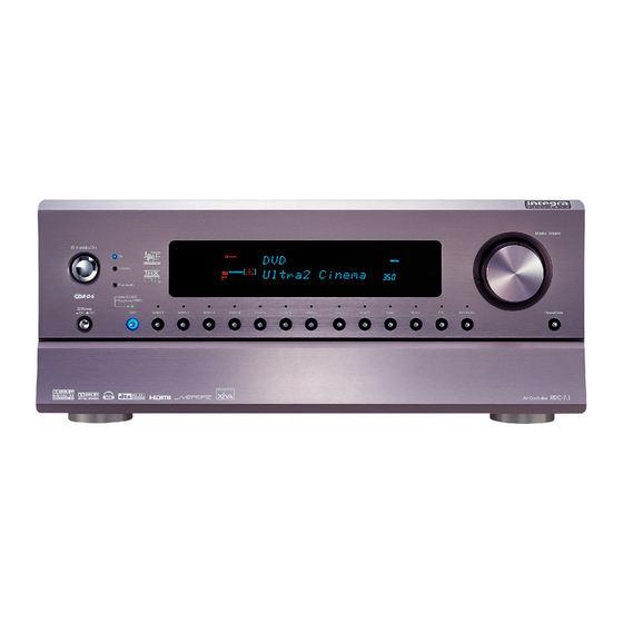
RDC-7.1
Titanium model
Q Q
3
6 7
1 3
120V AC, 60Hz
230-240V AC, 50Hz
220-230V AC, 50/60Hz
ON THE
.
9 4
2 8
Ref. No. 3869
Dec, 2004
1 5
0 5
8
2 9
9 4
RC-554M
RC-555M
m
co
RDC-7.1
9 9
2 8
9 9
Advertisement
Table of Contents

Related Manuals for Integra RDC-7.1


Summary of Contents for Integra RDC-7.1
- Page 1 RDC-7.1 3 7 63 1515 0 Ref. No. 3869 SERVICE MANUAL SERVICE MANUAL Dec, 2004 AV CONTROLLER RDC-7.1 MODEL Titanium model L 13942296513 RC-554M RC-555M UDD, UDT 120V AC, 60Hz 230-240V AC, 50Hz UPP-RC/RF, UPA 220-230V AC, 50/60Hz UGK, UGT...
-
Page 2: Specifications
RDC-7.1 3 7 63 1515 0 SPECIFICATIONS USA and Canadian models Amplifier Section General Maximum Output Level: 8.5 Vrms Power Supply Rating: AC 120 V, 60 Hz THD (Total Harmonic Distor- Consumption Power: 1.0 A Standby Power Consumption: 3.9 W tion): 0.05% (1 Vrms output) - Page 3 RDC-7.1 3 7 63 1515 0 SPECIFICATIONS USA and Canadian models Tuner Section Tuning frequency Range: 87.50 to 107.90 MHz, 200 kHz steps Usable Sensitivity: Stereo 17.2 dBf, 2.0 µV (75 IHF) 23 µV (75 DIN) Mono 11.2 dBf, 1.0 µV (75 IHF) 0.9 µV (75...
- Page 4 RDC-7.1 3 7 63 1515 0 SPECIFICATIONS Other than USA and Canadian models Amplifier Section General Maximum Output Level: 8.5 Vrms Power Supply Rating: AC 120 V, 60 Hz THD (Total Harmonic Distor- Consumption Power: 1.0 A Standby Power Consumption: 3.9 W...
- Page 5 RDC-7.1 3 7 63 1515 0 SPECIFICATIONS Other than USA and Canadian models Tuner Section Tuning frequency Range: 87.50 to 108.00 MHz, 50 kHz steps Usable Sensitivity: Stereo 17.2 dBf, 2.0 µV (75 IHF) 23 µV (75 DIN) Mono 11.2 dBf, 1.0 µV (75 IHF)
-
Page 6: Service Procedures
(On other than USA, Canadian, and Australian models, functions and operations. If interference generated by an external the RDC-7.1's Po wer switch must be set to On in order power supply, radio wave, or other electrical source results in to charge the backup system). Once it has been accident which causes the specified operations and functions to charged, the RDC-7.1 will retain the settings for several... - Page 7 DTR-10.5/RDC-7.1 3 7 63 1515 0 How to Install Updater (Operating environment: Windows XP or 2000) 0. Download the firmware "setup_xxxxxx.zip" to the disk top. 4. When Install is completed, this window appears. Double-click the icon. 1. Start Install program by double-clinking "Setup.exe".
- Page 8 DTR-10.5/RDC-7.1 3 7 63 1515 0 How to Use Updater 1. Connect your unit and PC with RS-232C cable, turn on 4. After completing update or skipping update by clicking "No(N)", the unit, and start "Updater". decide whether another one should be updated now or not.
-
Page 9: Exploded View
RDC-7.1 3 7 63 1515 0 EXPLODED VIEW-1 A451 A453 A324 x 5 pcs. A714 A324 A322 x 4 pcs. A318 A324 x 5 pcs. A320 A324 x 4 pcs. A316 A237 A151 L 13942296513 A233 U224 x 10 pcs. - Page 10 RDC-7.1 3 7 63 1515 0 EXPLODED VIEW-2 A095 A093 x 4 pcs. A461 x 23 pcs. x 16 pcs. A448 A091 x 29 pcs. A310 A312 A107 A101 x 2 pcs. A089 A449 A103 x 34 pcs. A431...
- Page 11 RDC-7.1 3 7 63 1515 0 EXPLODED VIEW-3 A021 x 4 pcs. Q9322B Q9311 Q9301 Q9322 A079 A455 x 3 pcs. P3106 Q9322A Q9351 A075 A077 x 4 pcs. A021 A039 x 4 pcs. A073 A053 x 3 pcs.
- Page 12 RDC-7.1 3 7 6 3 1 5 1 5 0 BLOCK DIAGRAM AUDIO SECTION SCH.16 NADG-8228 ETHER Q616 ETHER NET-TUNE CONTROL LEFT JUSTIFIED ETHER MAVERICK EP7312-CV Q606 Q3009 Q3501 Q604 Q603,Q608 FLASH TLC2932 EEPROM 8MB SDRAM 8MB SDRAM 32MB FLASH...
- Page 13 COMPOSITE VIDEO Q2035 Q2043 IN 6 REC SEL OUT 1 SVDEC3 Q2036 IN 7 Q2043 Q2040 OUT 2 Not use for RDC-7.1 Q2050 Y/C MIX MAIN SEL COMPOSITE VIDEO Q2213 Q2050 Q2230 IN 1 TK15420 Q2014 OUT 3 w w w...
- Page 14 RDC-7.1 3 7 6 3 1 5 1 5 0 BLOCK DIAGRAM 3 HDMI section Q8857 Q8102 EXT_CV ITU-RBT656/YUV24 ITU-RBT656/YUV24 Q8101 Q8801 H.V_SYNC H.V_SYNC EXT_S ADV7402 PIXCLK.BLANK PIXCLK.BLANK ADV73XX VIDEO VIDEO DECODER L8901~3 VFRESET ENCORDER I2C1 Q8103 Q8810 VDOFF...
-
Page 15: Audio Section
http://www.xiaoyu163.com 3 7 63 1515 0 BLOCK DIAGRAM AUDIO SECTION SCH.16 NADG-8228 ETHER Q616 ETHER NET-TUNE LEFT JUSTIFIED ETHER CONTROL MAVERICK EP7312-CV Q606 Q3009 Q3501 Q604 Q603,Q608 FLASH TLC2932 EEPROM 8MB SDRAM 32MB FLASH 8MB SDRAM 93LC46B HM5264165F HM5264165F MX29LV320 Q3004 IEEE1394 DSD 6CH... - Page 16 RDC-7.1 3 7 63 1515 0 11dB 11dB HEAD PHONE MASTER VOLUME Q4869~Q4871 90KLPF VLSC SCH. 5/6 NAAF-8156 SCH. 4 PREOUT Q4040~Q4047 Q4020 MUTE LEFT LEFT 90KLPF VLSC 192/24 RIGHT MUTE RIGHT NADG-8154 90KLPF VLSC SL->L SURROUND Q4023 MUTE...
-
Page 17: Block Diagram
Q2019 Q2019 ZONE2 OSD LC74761 -6dB IN 5 TC7W53FK Q2208 IN 6 REC SEL SVDEC3 IN 7 Not use for RDC-7.1 Q2050 MAIN SEL COMPOSITE VIDEO Q2050 IN 1 IN 2 IN 3 ZONE2 SEL u163 IN 4 IN 5... - Page 18 RDC-7.1 3 7 63 1515 0 VERT ) 1Vp-p Y/Cb/Cr COMPONENT VIDEO Q2228 OUT 1 P P P J-slot Q2603 Y/Cb/Cr OUT 2 Q2206 P P P From IN 4 (Component) Q2216 3-LINE Q2503 VIDEO Q2235 Y/C SEP CONVERTOR...
- Page 19 http://www.xiaoyu163.com 3 7 63 1515 0 BLOCK DIAGRAM 3 HDMI section Q8102 EXT_CV ITU-RBT656/YUV24 ITU-RBT656/YUV24 Q8101 Q8801 H.V_SYNC H.V_SYNC ADV7402 EXT_S PIXCLK.BLANK PIXCLK.BLANK ADV73XX VIDEO VIDEO DECODER L890 VFRESET ENCORDER I2C1 Q8103 EXT_HD 15MH Q8351 VCX162244FT ITU-RBT656/YUV24 H.V_SYNC PIXCLK.BLANK L 13942296513 SPDIF ITU-RBT656/YUV24 YUV4:2:2.16...
- Page 20 RDC-7.1 3 7 63 1515 0 Q8857 L8901~3 Q8810 VDOFF 5MHZ LPF X3 VDOFF YUV4:2:2.16 H.V_SYNC PIXCLK.BLANK L 13942296513 +5V REGULATOR Q8351 EV+5.6 +5V SUPPLY HDMI TRANSMITTER CLOCK GEN. YUV4:2:2.16 H.V_SYNC Q8301 12.288MHz PIXCLK.BLANK SII9190 Q8350 SPDIF CS8420 SAMPLE RATE...
- Page 21 RDC-7.1 3 7 6 3 1 5 1 5 0 TO NAAF-8145 (SCH.-2) P407A TO NAAF-8145 (SCH.-2) TO NAAF-8145 (SCH.-2) P408A P406A SCHEMATIC U033 NAAF-8146 NAAF-8144 DIAGRAM 1 P1863A P1865A P1864A P1863B P1865B P1864B Phono/AF IN/OUT MPC4570G2 R1540 1 to 3 sections...
- Page 22 RDC-7.1 3 7 6 3 1 5 1 5 0 TO NAETC-8146 (SCH.-1) TO NAETC-8146 (SCH.-1) TO NAETC-8146 (SCH.-1) SCHEMATIC P406B NAAF-8145 DIAGRAM 2 P408B P407B Z3VOLMUT AF IN 4 to 9 and MPC4570G2 Z2VOLMUT U032 R401 AI4L VZ2LSTB...
- Page 23 RDC-7.1/C-AES 3 7 6 3 1 5 1 5 0 SCHEMATIC DIAGRAM 3 Multi channel section NAAF-8150 SLOT E R1450 1.2K (Except US model/ +15V R1022 C1010 C1310 +15V 22/25 22/25 MPC4570G2 1/2W AGND BGND Option board: R1000 -15V...
- Page 24 RDC-7.1 3 7 6 3 1 5 1 5 0 SCHEMATIC DIAGRAM 4 DAC and Second PLL sections NADG-8154 +15V TO NAAR-8166 (SCH.-7) +15V P3106A R4271 R4110 R4130 R4150 DSD_FR-A BGND R4270 R4000 R4030 DSD_FL-A Q4000 -15V Q4010 Q4010 DSD_BCK-A 2.7K...
- Page 25 RDC-7.1 3 7 6 3 1 5 1 5 0 SCHEMATIC DIAGRAM 5 Preamplifier section TO NAAR-8166 (SCH.-7) NAAF-8156(1/2) P3105A Q4867 HPMUTE-B 2SC2712 TO NAETC-8214 C4300 VFLSTB-A (SCH.-14) 10/16 +15VAPOG C4350 100F R4933 P7506 BTLRL-A 220K C4650 R4380 BGND...
- Page 26 RDC-7.1 3 7 6 3 1 5 1 5 0 SCHEMATIC DIAGRAM 6 Output section NAAF-8156(2/2) FRONT FLPO-A FLPO-A LEFT BTLRL-A FRPO-A FRPO-A PREOUT A SWRLB FLPO-B FLPO-B FRONT SBSPB FRPO-B FRPO-B RIGHT CSPB CPO-A SRSPB FRSPB CPO-B CENTER...
- Page 27 RDC-7.1 3 7 6 3 1 5 1 5 0 SCHEMATIC DIAGRAM 7 SCH.-13 SCH.-15 SCH.-13 SCH.-12 SCH.15 SCH.-18 NAPS-8193 SCH.-18 NAETC-8184 FRONT VIDEO via U083 NAPS-8193 Mother section NAVD-8137 NAVD-8137 P3127B P3126B P3125B NAAR-8166 Q3106 Q3102 Q3116 T7S32F...
- Page 28 RDC-7.1 3 7 6 3 1 5 1 5 0 SCHEMATIC DIAGRAM 8 +3.3VDSP +3.3VDSP +5VDSP +5VDSP DIR section +5VDSP +3.3VDSP SLOT C +5VDAC +3.3VDAC +5VDAC Q7061 Optical C7001 C7075 DIRLRCK_M R7075 U7001 Q7001 MCLRCK R7076 47u/6.3 104Z C7012...
- Page 29 RDC-7.1 3 7 6 3 1 5 1 5 0 SCHEMATIC DIAGRAM 9 Second PLL section +3.3VDSP +5VDSP P7401 P7402A P7403A TO NAAR-8166 P7401B(SCH.-7) DSPMHS DSPMLFE DSPZHS DSPZLFE Z3PLLLOCK Z2PLLLOCK MPLLLOCK DSPMRST DSPDO DSPMCK DSPMLFE DSPCLK DSPBICK DSPBMC DSPMDI...
- Page 30 RDC-7.1 3 7 6 3 1 5 1 5 0 SCHEMATIC DIAGRAM 10 DSP section +1.65VDSPZ +1.65VDSP NADG-8163 +1.2VDSP +1.2VDSP Q7301C P7404A CVDD CVDD CVDD CVDD CVDD CVDD CVDD CVDD +3.3VDSP CVDD +3.3VDSP +3.3VDSP CVDD +3.3VDSP +1.2VDSP CVDD CVDD...
- Page 31 RDC-7.1 3 7 6 3 1 5 1 5 0 SCHEMATIC DIAGRAM 11 DSP section +3.3VDSP +3.3VDSP +3.3VDSP +1.2VDSPZ +3.3VDSP +1.2VDSPZ Q701C CVDD D701 D702 D703 D704 +3.3VDSP CVDD +3.3VDSP 1SS352 1SS352 1SS352 1SS352 CVDD Q701B P701 D705 CVDD...
- Page 32 RDC-7.1 3 7 6 3 1 5 1 5 0 SCHEMATIC DIAGRAM 12 Supply section U173 U172 NAPS-8194 NAPS-8195 TO NAAF-8156 P4864A (SCH.-5) NAETC-8180 1 3 9 4 2 2 9 6 5 1 3 w w w u 1 6 3...
- Page 33 RDC-7.1 3 7 6 3 1 5 1 5 0 SCHEMATIC DIAGRAM 13 Supply section NOTE THE COMPONENTS IDENTIFIED BY MARK ARE CRITICAL FOR SAFETY U177 NAETC-8199 REPLACE ONLY WITH PART NUMBER SPECIFIED. . VOLTAGE (MEASURED WITH VOLTMETER) IS DC VOLTAGE.(NO INPUT SIGNAL) .
- Page 34 RDC-7.1/C-AMFM 3 7 6 3 1 5 1 5 0 SCHEMATIC COAXIAL OUT COAXIAL IN COAXIAL IN US model:Option board:C-AMFM P7452 P7451 DIAGRAM 14 NADG-8159 P7453 NARF-8152 0*:Short Coaxial I/O and C7458 U084 102J Tuner sections C7457 C7456 C7455...
- Page 35 RDC-7.1 3 7 6 3 1 5 1 5 0 SCHEMATIC DIAGRAM 15 Display section P7501 TO NAAR-8166(SCH.-7) R7807 10K*15 C7801 103Z R7801 R7802 UPPER LOWER C7802 103Z P1-5 P37-41 P6-10 P42-46 C7803 104Z Q7602 P11-15 P47-51 FL_164 P16-20...
- Page 36 http://www.xiaoyu163.com RDC-7/C-NET-A 3 7 6 3 1 5 1 5 0 SCHEMATIC DIAGRAM 16 MultiMedia CPU +2.5V +5.6V +2.5V +3.3V NET-TUNE +3.3V +5.6V L603 P3102A Q601 BA33C25FP +3.3V NFM60R10T471 Address Bus (Except US L601 Main Memory Program Flash ROM +3.3V BLM21P221SG model/Option Data Bus...
- Page 37 RDC-7.1 3 7 6 3 1 5 1 5 0 SCHEMATIC DIAGRAM 17 IEEE1394 Q3501 MBM29LV800TA-90PFTN C3528 220/4 SLOT A 10K*4 Q3502 HD64F2367VF33 Q3503 Q3004 1 3 9 4 2 2 9 6 5 1 3 DTC114EE TSB43CA42PGF i-LINK...
- Page 38 RDC-7.1/C-HDMI 3 7 6 3 1 5 1 5 0 SCHEMATIC DIAGRAM 18 HDMI section SLOT L HDMI IN 1 (Except US model/ HDMI IN 2 R8106HS601 NAVD- P8501 E_Terminal P8601 E_Terminal R8112 R8735 #47K C8120 101J Option board:...
- Page 39 RDC-7.1/C-VIDEO 3 7 6 3 1 5 1 5 0 SCHEMATIC DIAGRAM 19 NAVD-8201 Video section VIDEO INPUT P2006 (Except US model SYNCDEC1 SYNCDEC2 C2151 104Z C2152 220/6.3 R2161 C2153 220/6.3 IN 1 MAIN Q2004 LC74761M-9848 Q2011 LC74761M-9848 ZONE2...
- Page 40 RDC-7.1/C-VIDEO 3 7 6 3 1 5 1 5 0 SCHEMATIC NAVD-8202 U182 DIAGRAM 20 SLOT I Video section Q2236 Q2225 Q2217 NPL-2P2A-DC24-177 RN1404 2SA1162GR MAX4018 D2201 D2208 D2205 D2212 D2203 D2204 D2210 D2202 1SS352 (Except US 2SC2712GR 1SS352...
- Page 41 RDC-7.1/C-CPNT-BNC 3 7 6 3 1 5 1 5 0 SCHEMATIC DIAGRAM 21 Video section (Except US model/Option board:C-CPNT-BNC) NAVD-8205 Q2501 SLOT J C2520 MAX4218 104Z R2504 R2559 C2517 C2521 OUTC R2508 R2505 INC- 220/16 104Z R2513 RL2501 INC+...
- Page 42 RDC-7.1 3 7 6 3 1 5 1 5 0 WIRING VIEW 1 P7453 P7451 P7452 P1861 NADG-8159 U085 P1860 P1862 U084 P105 SLOT D P1401 P1400 SCHEMATIC 14 P3108A P7454B P1405 NAETC-8160 P7454A P7002A NAAF-8144 NADG-8162 FM_VSM SLOT F...
- Page 43 RDC-7.1 3 7 6 3 1 5 1 5 0 WIRING VIEW 2 FRONT PANEL & PRE-AMPLIFIER SECTIONS U222 P7501 P7503B P7503A NADIS-8212 SCHEMATIC 15 NAETC-8213 SCHEMATIC 15 U7501 STANDBY SWITCH U225 DISPLAY CIRCUIT NAETC-8216 U224 DOOR MOTOR NAETC-8215...
- Page 44 RDC-7.1 3 7 6 3 1 5 1 5 0 WIRING VIEW 3 P4872A POWER SUPPLY SECTION J4801E P3105A J4801D NAAF-8156 PRE-AMPLIFIER PRIMARY SCHEMATIC 5/6 CIRCUIT P9111 P9112 POWER SWITCH T9002 NAPS-8196 SCHEMATIC 13 P9006B P9005B U175 BLACK P9005A...
- Page 45 http://www.xiaoyu163.com TX-NR1000 3 7 63 1515 0 IC BLOCK DIAGRAM AND DESCRIPTION AK4114VQ(192kHz 24bit Digital Audio Interface Transceiver) Block Diagram AVSS AVDD X'tal Clock Oscillator 8 to 3 Recovery Clock MCKO1 Generator MCKO2 Input Selector LRCK DAIF Audio BICK Decoder SDTO DAUX DVDD...
- Page 46 http://www.xiaoyu163.com TX-NR1000 3 7 63 1515 0 IC BLOCK DIAGRAM AND DESCRIPTION AK4114VQ(192kHz 24bit Digital Audio Interface Transceiver) No. Symbol Function Receiver channel input 4 pin NC(AVSS) No connection pin Receiver channel input 5 pin TEST2 Test 2 pin Receiver channel input 6 pin NC(AVSS) No connection pin Receiver channel input 7 pin...
- Page 47 http://www.xiaoyu163.com TX-NR1000 3 7 63 1515 0 IC BLOCK DIAGRAM AND DESCRIPTION AK4584VF(107dB 24-Bit 96kHz 4-Channel SDC) AVDD AVSS DVDD DVSS TVDD LIN2+ LIN1+ LIN1+ LRCK ∆Σ Decimation LIN2- LIN1- LIN1- Modulator Filter BICK RIN2+ RIN1+ RIN2- RIN1- SDTO1 RIN1+ ∆Σ...
- Page 48 http://www.xiaoyu163.com TX-NR1000 3 7 63 1515 0 IC BLOCK DIAGRAM AND DESCRIPTION AK4585AVF(24-Bit 192kHz ∆Σ ADC) VCOM M/S DFS1 DFS0 CKS1 CKS0 VREFL VREFR VREFL AVSS AVSS VCOM TEST LIN+ LIN+ RIN+ Delta-Sigma Decimation LIN- RIN- LIN- Modulator Filter LRCK CKS0 AVDD BICK...
-
Page 49: Block Diagram
http://www.xiaoyu163.com TX-NR1000 3 7 63 1515 0 IC BLOCK DIAGRAMS AND TERMINAL DESCRIPTIONS BU1924FS (RDS Decoder) <European model only> BLOCK DIAGRAM 100k 120k 8th Switched 100k capacitor filter comparator anti-aliasing filter Vref RCLK (16) Analog Power supply QUAL RDATA Bi-phase Differential 57kHz (12) - Page 50 http://www.xiaoyu163.com TX-NR1000 3 7 63 1515 0 IC BLOCK DIAGRAM AND DESCRIPTION CS8420(Digital audio sample rate converter) COPY ORIG DFC0,DFC1...Data flow control inputs DFC0 DFC1 OMCK..Output section master clock input L 13942296513 SDIN..Serial audio input port data input EMPH/U SCLK...Serial audio input port bit clock input ILRCK...Serial audio input port left/right clock input SDOUT..Serial audio output port data output OSCLK..Serial audio output port bit clock input or output...
-
Page 51: Pin Descriptions
http://www.xiaoyu163.com TX-NR1000 3 7 63 1515 0 IC BLOCK DIAGRAM AND DESCRIPTION IC42S16800-7T(2Mx8 bitsx4 banks Synchronus Dynamic RAM) PIN DESCRIPTIONS PIN CONFIGURATIONS 54-Pin TSOP-2 (IC42S16800) Pin Name Function Master Clock Clock Enable DQ15 VDDQ VSSQ Chip Select DQ14 DQ13 Row Address Strobe VSSQ VDDQ DQ12... -
Page 52: Pin Functions
http://www.xiaoyu163.com TX-NR1000 3 7 63 1515 0 IC BLOCK DIAGRAM AND DESCRIPTION IC42S16800-7T(2Mx8 bitsx4 banks Synchronous Dynamic RAM) PIN FUNCTIONS Symbol Type Function (In Detail) Input Pin Master Clock: Other inputs signals are referenced to the CLK rising edge Input Pin Clock Enable: CKE HIGH activates, and CKE LOW deactivates internal clock signals,device input buffers and output drivers. - Page 53 http://www.xiaoyu163.com TX-NR1000 3 7 63 1515 0 IC BLOCK DIAGRAM AND DESCRIPTION MM1117XFBE(3 inputs/1 output video switch) BUFFER Control Input Truth Table CLAMP CLAMP CLAMP L 13942296513 u163 http://www.xiaoyu163.com...
- Page 54 http://www.xiaoyu163.com TX-NR1000 3 7 63 1515 0 IC BLOCK DIAGRAM AND DESCRIPTION MX29LV160BBTC-70(16Mbit CMOS single voltage 3V only flash memory) PIN CONFIGURATIONS PIN DESCRIPTION 48 TSOP (Standard Type) (12mm x 20mm) SYMBOL PIN NAME A0~A19 Address Input BYTE Q0~Q14 Data Input/Output Q15/A-1 Q15/A-1 Q15(Word mode)/LSB addr(Byte mode)
- Page 55 http://www.xiaoyu163.com TX-NR1000 3 7 63 1515 0 IC BLOCK DIAGRAM AND DESCRIPTION PCA9564PW(Parallel bus to I C-bus controller) PIN CONFIGURATION Ð SO, TSSOP PIN CONFIGURATION PIN NUMBER SYMBOL NAME AND FUNCTION SO, TSSOP HVQFN TYPE 1, 2, 3, 4, 5, 1, 2, 3, 4, D0±D7 Data Bus: Bi-directional 3-State data bus used to transfer commands, data and status...
- Page 56 http://www.xiaoyu163.com TX-NR1000 3 7 63 1515 0 IC BLOCK DIAGRAM AND DESCRIPTION SM5819AF(6-channel DSD-PCM converter) DSIFL DSIFR DSICT FIR FILTER DSISL MUTE DSISR DOWN DSISW SAMPLING UNIT DSGAIN VDDL SEL1FS DSBCK POFUR FMTPCM SEL4FS DSIFL POCSW DSIFR POSLR 24bit 720 word DSICT PLRCK (fs 240w)
- Page 57 http://www.xiaoyu163.com TX-NR1000 3 7 63 1515 0 IC BLOCK DIAGRAM AND DESCRIPTION TC90A69F(3-lines digital COM filter) PLL DET VCO I CBUS 4fsc 8fsc 8fsc CORING V-ENHANCER CORING Ped. DELAY PEAKING CLIP LINE LINE INTERPOLATION KILLER MEMORY MEMORY DYNAMIC COMB C-N.C FILTER Sync Clamp L 13942296513...
- Page 58 http://www.xiaoyu163.com TX-NR1000 3 7 63 1515 0 IC BLOCK DIAGRAM AND DESCRIPTION TC9162BFG(Function Switch) COM1 COM1 COM2 COM2 COM3 COM3 L 13942296513 COM4 COM4 DATA SHIFT REGISTER Symbol Pin No. Function Negative power supply Ground Positive power supply S1~S7 Input/output terminals 2,3,5,6,8,9,11 S1~S7 Input/output terminals...
- Page 59 http://www.xiaoyu163.com TX-NR1000 3 7 63 1515 0 IC BLOCK DIAGRAM AND DESCRIPTION TC9163BFG(Function Switch) COM1 COM1 COM2 COM2 L 13942296513 COM4 COM4 DATA SHIFT REGISTER Symbol Pin No. Function Negative power supply Ground Positive power supply S1~S8 Input/output terminals 2,3,4,6,7,8,10,11 S1~S8 Input/output terminals 27,26,25,23,22,21,18,17...
- Page 60 http://www.xiaoyu163.com TX-NR1000 3 7 63 1515 0 IC BLOCK DIAGRAM AND DESCRIPTION TC9164BFG(Function Switch) COM1 COM1 COM2 COM2 L 13942296513 COM4 COM4 DATA SHIFT REGISTER Symbol Pin No. Function Negative power supply Ground Positive power supply S1~S8 Input/output terminals 2,3,4,5,7,8,10,11 S1~S8 Input/output terminals 27,26,25,24,22,21,18,17...
- Page 61 http://www.xiaoyu163.com TX-NR1000 3 7 63 1515 0 IC BLOCK DIAGRAMS AND DESCRIPTIONS TC9246F(PLL IC for Digital Audio) LOCK LOCK DETECTION MICROPROCESSOR INTERFACE CIRCUIT PROGRAMMABLE COUNTER L 13942296513 AMPI AMPO Symbol Function Description Reference signal input pin Phase error signal output pin VDDA Analog power supply AMPI...
- Page 62 http://www.xiaoyu163.com TX-NR1000 3 7 63 1515 0 IC BLOCK DIAGRAM AND DESCRIPTION TC9274FG-023 (Analog switch) R - c h S5 S6 S7 S8 S9 S10 S11 S12 S13 S14 S15 33 32 31 30 29 28 27 26 25 24 23 S5 S6 S7 S8 S9 S10 S11 S12 S13 S14 S15 3 3 3 2 3 1 3 0 2 9 2 8 2 7 2 6 2 5 2 4 2 3 S 1 6...
- Page 63 http://www.xiaoyu163.com TX-NR1000 3 7 63 1515 0 IC BLOCK DIAGRAM AND DESCRIPTION TC94A46FG(Function Switch) Latch Latch Latch Latch Latch Latch Latch Latch L 13942296513 TIMING COM1 COM1 GENERATION COM2 COM2 LEVEL SHIFT CIRCUIT u163 http://www.xiaoyu163.com...
- Page 64 http://www.xiaoyu163.com TX-NR1000 3 7 63 1515 0 IC BLOCK DIAGRAM AND DESCRIPTION TC94A46FG(Function Switch) PIN NO. SYMBOL TERMINAL FUNCTION/OPERATION Analog Switch Circuit Input/ Output Terminals COM1 Output/ COM2 Input L 13942296513 Terminals COM3 Negative power Power supply terminal. Positive power Digital ground Input to change a chip select code.
- Page 65 http://www.xiaoyu163.com TX-NR1000 3 7 63 1515 0 IC BLOCK DIAGRAM AND DESCRIPTION TLC2932IPWLE(High-Performance Phase-Locked Loop) PW PACKAGE (TOP VIEW) LOGIC V VCO V SELECT BIAS VCO OUT VCO IN FIN ±A VCO GND FIN ±B VCO INHIBIT PFD OUT PFD INHIBIT LOGIC GND Terminal Functions TERMINAL...
- Page 66 http://www.xiaoyu163.com TX-NR1000 3 7 63 1515 0 IC BLOCK DIAGRAM AND DESCRIPTION WM8716(24 bit 192kHz Stereo DAC) MODE ML/12S MC/DM1 MD/DM0 DIFFHW MUTEB CSB/WO RSTB ZERO MODEBX AGNDR AVDDR (24) (28) (27) (26) (17) (25) (23) (22) (21) (12) (10) (11) VMIDR CONTROL INTERFACE ML/12S...
- Page 67 http://www.xiaoyu163.com TX-NR1000 3 7 63 1515 0 IC BLOCK DIAGRAM AND DESCRIPTION WM8719(24 bit differential stereo DAC with volume control) LATCH SDIN SCLK SDOUT ZEROFR ZEROFL LRCLK LATCH BCLK CONTROL INTERFACE SCLK MCLK PCM/DSD SDIN SDOUT VOUTRP BCKIN SIGMA DVDD RIGHT DELTA LRCIN...
-
Page 68: Pin Configuration
http://www.xiaoyu163.com TX-NR1000 3 7 63 1515 0 WM8816(Stereo Digital Volume Control) BLOCK DIAGRAM PIN CONFIGURATION AGND AVDD LGND LEFT OUT Peak Zero Level Crossing Control RGND LGND Detector DGND CCLK DVDD External Opamp WM8816 MUTEB DATA MUTEB Control DATA CCLK Zero Peak Crossing... -
Page 69: Disassembling Procedures
RDC-7.1 3 7 63 1515 0 DISASSEMBLING PROCEDURES 1 3.Removement of Slot PC boards 1.Top covers/Side panels Remove 2 special screws E using Allen (Hexagon) Remove 10 decorative screws A to release Top covers wrench to release Slot A. - Page 70 RDC-7.1 3 7 63 1515 0 DISASSEMBLING PROCEDURES 2 5.Main microprocessor PC board 4.Rail A Remove Rail A. Remove Slot PC boards except Slot CD and FG PC board. Remove 2 Special screws J fixed RS232 terminal. Remove 34 copper screws H (30 on the top face, 4 on the Remove 15 screws G on Slot CD and remove Plate CD.
-
Page 71: Packing View
RDC-7.1 3 7 63 1515 0 PACKING VIEW 1 A704 A706 A711 A501 A708 A711 Accessory assembly Instruction A710*8 manuals (European model only) Instruction manuals (European model only) A700 L 13942296513 A700 A709 A750 A709 u163 A754 http://www.xiaoyu163.com... - Page 72 RDC-7.1 3 7 63 1515 0 PACKING VIEW 2 A807 A866 Speaker Cable A853 Insert A807 between page 1 & 2 A731 of A853. A872 A854 A860 P9002 A861 A871 A804 A800 L 13942296513 A802 A804 A806 A707 A851 u163 http://www.xiaoyu163.com...
- Page 73 RDC-7.1 3 7 63 1515 0 PACKING VIEW 2 (European model only) A853 A854 A807 A855 A856 Speaker Cable A857 A858 A872 P9002 A871 A850 A804 A800 A804 L 13942296513 A802 A804 A806 A859 A860 A861 A862 A731 A707...
-
Page 74: Exploded View Parts List
RDC-7.1 3 7 6 3 1 5 1 5 0 EXPLODED VIEW-PARTS LIST NOTE: THE COMPONENTS IDENTIFIED BY MARK ! ARE CRITICAL FOR RISK OF FIRE AND ELECTRIC SHOCK. REPLACE ONLY WITH PART NUMBER SPECIFIED. NOTE: <D>: USA model only <P>: European model only <A>:Australian model only <DT>: 120V model only <GT>: 220V model only <K>:Korean model only... - Page 75 RDC-7.1 3 7 6 3 1 5 1 5 0 A073 27141905 Retainer HS A075 801612 3TTB+8B(CU),Self-tapping screw A077 27141904 Retainer AC A079 801612 3TTB+8B(CU),Self-tapping screw A083 27130933 Bracket rail A A085 27130935 Bracket bottom A087 801612 3TTB+8B(CU),Self-tapping screw...
- Page 76 RDC-7.1 3 7 6 3 1 5 1 5 0 A165 27141759 Retainer W A167 834426068 2.6TTS+6B(BC),Self-tapping screw A169 27141752 Retainer S A171 24804045B Motor with gear A173 82143006 3P+6FN(BC),Pan head screw A177 28141426 t1.5*25*5,Cushion A179 28141430 Cushion A181...
- Page 77 RDC-7.1 3 7 6 3 1 5 1 5 0 A310 25060151 Terminal GND A312 87643010 W3*10F(BC),Flat washer A314 28135293 Badge A316 28185445B Side panel L A317 28141566 T4*L20*D10,Cushion A318 28185446B Side panel R A319 28141566 T4*L20*D10,Cushion A320 28145180...
- Page 78 RDC-7.1 3 7 6 3 1 5 1 5 0 29363793 Label, cover <P/DT/GT/A/K> A454 27160542 Heat sink S A455 27225156 Shield case A <P/DT/GT/A/K> A457 27225157 Shield case B <P/DT/GT/A/K> A459 801612 3TTB+8B(CU),Self-tapping screw A461 801620A Special screw, plate <P/DT/GT/A/K>...
- Page 79 RDC-7.1 3 7 6 3 1 5 1 5 0 Q9351 222780565JRC 78M56(NJM78M56FA),IC Q9404 2202304 or 2SC4512-Y or 2202305 2SC4512-P,Transistor Q9404A 223026 Isolated sheet Q9404B 223034 MT-25,Transistor accessory Q9411 222780054JRC 7805FA(NJM7805FA),IC Q9432,Q9442 2202364 or 2SA1693-Y or 2202363 or 2SA1693-O or...
- Page 80 RDC-7.1 3 7 6 3 1 5 1 5 0 1A989593-1D NAPS-8193-1D,Power supply circuit PC board ass'y <DT> 1A989593-1E NAPS-8193-1E,Power supply circuit PC board ass'y <A> U172 1A989594-1A NAPS-8194-1A,Constant voltage PC board ass'y <D> 1A989594-1B NAPS-8194-1B,Constant voltage PC board ass'y <P>...
- Page 81 RDC-7.1 3 7 6 3 1 5 1 5 0 REF. NO. PART NO. DESCRIPTION A700 29092161 Pad ass'y A704 29095964 0.515*1350*1500,Sheet A706 29100035-1 720*1020,Poly-bag A707 29054166 Carton, accessory A708 29110149 Tape , cellophane A709 29110148 PP tape A710...
- Page 82 RDC-7.1 3 7 6 3 1 5 1 5 0 253298KAW AS-CEE-3,Power supply cord <P/GT/K> 253391VOL AS-SAA, Power supply cord <A> L 1 3 9 4 2 2 9 6 5 1 3 u 1 6 3 http://www.xiaoyu163.com...
-
Page 83: Printed Circuit Board-Parts List
http://www.xiaoyu163.com 3 7 6 3 1 5 1 5 0 PRINTED CIRCUIT BOARD-PARTS LIST NOTE: THE COMPONENTS IDENTIFIED BY MARK ! ARE CRITICAL FOR RISK OF FIRE AND ELECTRIC SHOCK. REPLACE ONLY WITH PART NUMBER SPECIFIED. Note: <D>:120V model only <GT>:Asian model for 220V <P>:European model only <DT>: Asian model for 120V <A>:Australian model only <K>:Korean model only <O>:Except 120V model... - Page 84 http://www.xiaoyu163.com 3 7 6 3 1 5 1 5 0 Q8308,Q8505,Q8605 2216400R2 2SB1132 Q8309,Q8503 226066R2 UM6K1N,Array Q8506,Q8606 2216390R2 DTC144EE Q8507,Q8607 2216380R2 DTA144EE Q8508,Q8603 226066R2 UM6K1N,Array Q8509,Q8858 2216520R2 2SK3019 Q8901,Q8902,Q8903 2214375R2 2SA1162-GR Diodes D8101,D8102,D8103 223266R2 1SS226 D8104,D8105,D8106 223266R2 1SS226 D8701 223269R2 1SS355 Coils L8001,L8002,L8003...
- Page 85 http://www.xiaoyu163.com 3 7 6 3 1 5 1 5 0 C8025,C8026,C8027 332181050R1 CK725F1A-105Z1,Chip ceramic C8028,C8029,C8031 332181050R1 CK725F1A-105Z1,Chip ceramic C8030,C8035,C8119 342101024R1 CC725CH1H-102J1,Chip ceramic C8032,C8078,C8142 356742209R2 CEWX16V-22M,Chip elect. C8033,C8040,C8045 332181050R1 CK725F1A-105Z1,Chip ceramic C8034,C8120 342101014R1 CC725CH1H-101J1,Chip ceramic C8036,C8038 342101204R1 CC725CH1H-120J1,Chip ceramic C8041,C8042,C8043 3567A2219R2 CEWX4V-220M,Chip elect.
- Page 86 http://www.xiaoyu163.com 3 7 6 3 1 5 1 5 0 C8406,C8425,C8516 342101024R1 CC725CH1H-102J1,Chip ceramic C8407,C8408,C8409 332181050R1 CK725F1A-105Z1,Chip ceramic C8410,C8411,C8413 332181050R1 CK725F1A-105Z1,Chip ceramic CIRCUIT NO. PART NO. DESCRIPTION Capacitors C8414,C8415,C8417 332181050R1 CK725F1A-105Z1,Chip ceramic C8418,C8421,C8423 3567A2219R2 CEWX4V-220M,Chip elect. C8419,C8420,C8422 332181050R1 CK725F1A-105Z1,Chip ceramic C8424,C8426,C8427 332181050R1 CK725F1A-105Z1,Chip ceramic...
- Page 87 http://www.xiaoyu163.com 3 7 6 3 1 5 1 5 0 C8905 332161040R1 CK725F1E-104Z1,Chip ceramic C8908,C8909,C8910 356723319R2 CEWX6.3V-330M,Chip elect. R8354 332161040R1 CK725F1E-104Z1,Chip ceramic Resistors R8341 433421004R1 RN72K2E-100JD,Chip carbon R8001,R8002,R8003 435032204R1 RN72K1J-220JE,Chip carbon R8004,R8005,R8006 43484710004R2 RM7LJ100X04,CR array R8007,R8008,R8009 43484710004R2 RM7LJ100X04,CR array R8010,R8011 43484710004R2 RM7LJ100X04,CR array R8013...
- Page 88 http://www.xiaoyu163.com 3 7 6 3 1 5 1 5 0 R8155,R8156,R8157 435031044R1 RN72K1J-104JE,Chip carbon R8165,R8166,R8167 435032204R1 RN72K1J-220JE,Chip carbon R8168,R8169,R8170 435031024R1 RN72K1J-102JE,Chip carbon R8171,R8172,R8307 435031024R1 RN72K1J-102JE,Chip carbon R8173,R8174,R8175 435030004R1 RN72K1J-000JE,Chip carbon R8183,R8184,R8185 43484722004R2 RM7LJ220X04,CR array R8186 43484722004R2 RM7LJ220X04,CR array R8187,R8188,R8189 435032204R1 RN72K1J-220JE,Chip carbon R8190 435032204R1...
- Page 89 http://www.xiaoyu163.com 3 7 6 3 1 5 1 5 0 R8524,R8525,R8526 43484722004R2 RM7LJ220X04,CR array R8527,R8528,R8529 43484722004R2 RM7LJ220X04,CR array R8530,R8630 435033914R1 RN72K1J-391JE,Chip carbon R8533,R8633,R8738 435034734R1 RN72K1J-473JE,Chip carbon R8602,R8604,R8606 435034724R1 RN72K1J-472JE,Chip carbon R8607,R8641,R8708 435030004R1 RN72K1J-000JE,Chip carbon CIRCUIT NO. PART NO. DESCRIPTION Resistors R8609,R8632,R8639 435034724R1 RN72K1J-472JE,Chip carbon...
- Page 90 http://www.xiaoyu163.com 3 7 6 3 1 5 1 5 0 R8913,R8914,R8915 435034712R1 RN72K1J-471FE,Chip carbon R8918 435030004R1 RN72K1J-000JE,Chip carbon R8920,R8921 435031034R1 RN72K1J-103JE,Chip carbon R8922,R8923,R8924 435034712R1 RN72K1J-471FE,Chip carbon R8925,R8927,R8928 435035624R1 RN72K1J-562JE,Chip carbon R8929,R8930,R8931 435034712R1 RN72K1J-471FE,Chip carbon R8932,R8933,R8934 435031024R1 RN72K1J-102JE,Chip carbon Terminals P8302,P8501,P8601 25052956R3 DC1R019JDA,HDMI Plugs...
- Page 91 http://www.xiaoyu163.com 3 7 6 3 1 5 1 5 0 2216220R2 KRA102S Capacitors C1460,C1461 373022214R2 ECHU50V-221J,Chip film C1465,C1466,C1470 395924707 CE04W6.3V-47M(RFS),Elect. C1471,C1600,C1601 395924707 CE04W6.3V-47M(RFS),Elect. C1475,C1476,C1525 395941007 CE04W16V-10M(RFS),Elect. C1480,C1481 373021524R2 ECHU50V-152J,Chip film C1485,C1486 342101014R1 CC725CH1H-101J1,Chip ceramic C1490,C1491 373021234R2 ECHU50V-123J,Chip film C1495,C1496,C1685 393341007 or CE04W16V-10M(VX) or 394641007 CE04W16V-10M(VR),Elect.
- Page 92 http://www.xiaoyu163.com 3 7 6 3 1 5 1 5 0 394664707 CE04W35V-47M(VR),Elect. C1863 342103314R1 CC725CH1H-331J1,Chip ceramic C1864,C1865 332161040R1 CK725F1E-104Z1,Chip ceramic C1866,C1867 332161040R1 CK725F1E-104Z1,Chip ceramic C1868 393324707 or CE04W6.3V-47M(VX) or 394624707 CE04W6.3V-47M(VR),Elect. C1880,C1881 395852207 CE04W25V-22M(ROB),Elect. C1890,C1891 395824707 CE04W6.3V-47M(ROB),Elect. C1900,C1901,C1902 342103304R1 CC725CH1H-330J1,Chip ceramic C1903,C1904,C1905 342103304R1 CC725CH1H-330J1,Chip ceramic...
- Page 93 http://www.xiaoyu163.com 3 7 6 3 1 5 1 5 0 R1520,R1521 435022234R1 RN72W1J-223JE,Chip carbon R1530,R1531 435021224R1 RN72W1J-122JE,Chip carbon R1535,R1536,R1705 435024744R1 RN72W1J-474JE,Chip carbon R1540,R1541,R1660 435021004R1 RN72W1J-100JE,Chip carbon R1551,R1580,R1581 435023314R1 RN72W1J-331JE,Chip carbon R1561,R1590,R1591 435025634R1 RN72W1J-563JE,Chip carbon R1570,R1571,R1600 435022244R1 RN72W1J-224JE,Chip carbon R1601,R1630,R1631 435022244R1 RN72W1J-224JE,Chip carbon R1610,R1611 435023314R1...
- Page 94 http://www.xiaoyu163.com 3 7 6 3 1 5 1 5 0 R453,R454,R455,R456 435022214R1 RN72W1J-221JE,Chip carbon R457,R458 435023314R1 RN72W1J-331JE,Chip carbon R459,R460 435025634R1 RN72W1J-563JE,Chip carbon R461,R462,R473,R474 435022244R1 RN72W1J-224JE,Chip carbon R463,R464 443622204 RS1WBJ-22,Metal oxide R475,R476 435021034R1 RN72W1J-103JE,Chip carbon R477,R478 435024724R1 RN72W1J-472JE,Chip carbon R479,R480 435021024R1 RN72W1J-102JE,Chip carbon R481 435030004R1...
- Page 95 http://www.xiaoyu163.com 3 7 6 3 1 5 1 5 0 D1418,D1419,D1420 223234R2 or 1SS352 or D1421,D1422,D1423 223269R2 1SS355 D1424,D1425,D1426 223234R2 or 1SS352 or D1427,D1428,D1429 223269R2 1SS355 D1430,D1431 223234R2 or 1SS352 or 223269R2 1SS355 Coils L1400,L1401,L1402 231237M022R2 or NCH-1471 or L1403,L1405 233533M022R2 NCH-1587-022M L1404,L1406...
- Page 96 http://www.xiaoyu163.com 3 7 6 3 1 5 1 5 0 C1371,C1372 395824707 CE04W6.3V-47M(ROB),Elect. C1375,C1376 395824707 CE04W6.3V-47M(ROB),Elect. C1414,C1416,C1419 332161040R1 CK725F1E-104Z1,Chip ceramic C1415,C1428 393380227 CE04W50V-2.2M(VX),Elect. C1417,C1420,C1430 393341007 or CE04W16V-10M(VX) or 394641007 CE04W16V-10M(VR),Elect. C1418,C1433 342101014R1 CC725CH1H-101J1,Chip ceramic C1421,C1423,C1424 332161040R1 CK725F1E-104Z1,Chip ceramic C1422,C1438 393321017 or CE04W6.3V-100M(VX) or 394621017 CE04W6.3V-100M(VR),Elect.
- Page 97 http://www.xiaoyu163.com 3 7 6 3 1 5 1 5 0 R1304,R1305 435024724R1 RN72W1J-472JE,Chip carbon R1306,R1307 435024724R1 RN72W1J-472JE,Chip carbon R1311,R1312,R1313 435023314R1 RN72W1J-331JE,Chip carbon R1314,R1315,R1316 435023314R1 RN72W1J-331JE,Chip carbon R1317,R1320,R1321 435023314R1 RN72W1J-331JE,Chip carbon R1322,R1323,R1324 435023314R1 RN72W1J-331JE,Chip carbon R1325,R1326,R1327 435023314R1 RN72W1J-331JE,Chip carbon R1332,R1333,R1334 435025634R1 RN72W1J-563JE,Chip carbon R1335,R1336,R1338 435025634R1...
- Page 98 http://www.xiaoyu163.com 3 7 6 3 1 5 1 5 0 C102 345021014 CC45SL50V-101J,Ceramic C104 335622230 CK45F50V-223Z,Ceramic C107 335622230 CK45F50V-223Z,Ceramic <P> C108,C114 393321017 or CE04W6.3V-100M(VX) or 394621017 CE04W6.3V-100M(VR),Elect. <P> C109,C110 345343304 CC45CH50V-330J,Ceramic <P> C111 374725614 ECQ-B50V-561J,Plastic film <P> C113 345022714 CC45SL50V-271J,Ceramic <P> C115 335622230 CK45F50V-223Z,Ceramic...
- Page 99 http://www.xiaoyu163.com 3 7 6 3 1 5 1 5 0 Q4863 22241895R2 TC7SZ125FU Q4864 222118A CC1536 Q4865,Q4866 222740077R2TO TC74HCT7007AF Q4882 222780055JRC or 78M05(NJM78M05FA) or 222780055MAT or 78M05(AN78M05F) or 222780055NEC 78M05HF(MPC78M05HF) Coils L4000,L4002,L4003 231237M022R2 or NCH-1471 or L4005,L4007,L4010 233533M022R2 NCH-1587-022M L4012,L4013,L4015 231237M022R2 or NCH-1471 or L4017,L4864...
- Page 100 http://www.xiaoyu163.com 3 7 6 3 1 5 1 5 0 C4103,C4104,C4105 374724714 ECQ-B50V-471J,Plastic film C4106,C4107 374724714 ECQ-B50V-471J,Plastic film C4108,C4109 374724714 ECQ-B50V-471J,Plastic film C4150,C4151,C4152 395852207 CE04W25V-22M(ROB),Elect. C4153,C4154,C4155 395952207 CE04W25V-22M(RFS),Elect. C4156,C4157 395852207 CE04W25V-22M(ROB),Elect. C4158,C4159 395952207 CE04W25V-22M(RFS),Elect. C4160,C4162,C4163 393341007 or CE04W16V-10M(VX) or C4165,C4167 394641007 CE04W16V-10M(VR),Elect.
- Page 101 http://www.xiaoyu163.com 3 7 6 3 1 5 1 5 0 R4043,R4044,R4045 435022724R1 RN72W1J-272JE,Chip carbon R4046,R4047 435022724R1 RN72W1J-272JE,Chip carbon R4048,R4049 435022724R1 RN72W1J-272JE,Chip carbon R4050,R4052,R4053 435022204R1 RN72W1J-220JE,Chip carbon R4055,R4057,R4060 435022204R1 RN72W1J-220JE,Chip carbon R4062,R4063,R4065 435022204R1 RN72W1J-220JE,Chip carbon R4067,R4070,R4072 435022204R1 RN72W1J-220JE,Chip carbon R4073,R4075,R4077 435022204R1 RN72W1J-220JE,Chip carbon R4080,R4082,R4083 435022204R1...
- Page 102 http://www.xiaoyu163.com 3 7 6 3 1 5 1 5 0 R4181,R4182,R4183 435021524R1 RN72W1J-152JE,Chip carbon R4184,R4185,R4186 435021524R1 RN72W1J-152JE,Chip carbon R4187,R4188,R4189 435021524R1 RN72W1J-152JE,Chip carbon R4230,R4231,R4232 435021024R1 RN72W1J-102JE,Chip carbon R4233,R4234,R4235 435021024R1 RN72W1J-102JE,Chip carbon R4236,R4237,R4238 435021024R1 RN72W1J-102JE,Chip carbon R4239,R4260,R4261 435021024R1 RN72W1J-102JE,Chip carbon R4240,R4241,R4242 435025634R1 RN72W1J-563JE,Chip carbon R4243,R4244,R4245 435025634R1...
- Page 103 http://www.xiaoyu163.com 3 7 6 3 1 5 1 5 0 Resistors R4903 435024724R1 RN72W1J-472JE,Chip carbon R4909,R4910,R4912 435023314R1 RN72W1J-331JE,Chip carbon R4911 435022734R1 RN72W1J-273JE,Chip carbon R4914,R4915,R4916 443621504 RS1WBJ-15,Metal oxide R4944,R4945,R4946 435030004R1 RN72K1J-000JE,Chip carbon R4947,R4948 435030004R1 RN72K1J-000JE,Chip carbon Plugs P3106A 25056359R2 MINI-CT-38P(3-353315-8) P4861 25055038 NPLG-2P29 P4871...
- Page 104 http://www.xiaoyu163.com 3 7 6 3 1 5 1 5 0 Q4063,Q4064,Q4065 2215410R2 RN1441 Q4066,Q4067,Q4070 2215410R2 RN1441 Q4071,Q4072,Q4073 2215410R2 RN1441 Q4074,Q4075, Q4076 2215410R2 RN1441 Q4077,Q4090,Q4091 2215410R2 RN1441 Q4100,Q4101 2215410R2 RN1441 Q4110,Q4111 2215410R2 RN1441 Q4160,Q4867,Q4872 2213145R2 or 2SC2712-GR or Q4874,Q4881 2216175R2 KTC3875-GR Q4868,Q4873,Q4875 2214530R2 or RN2402 or...
- Page 105 http://www.xiaoyu163.com 3 7 6 3 1 5 1 5 0 C340,C341,C342 395852207 CE04W25V-22M(ROB),Elect. C352,C353 342111024R1 CC725CH1E-102J1,Chip ceramic C4250,C4251,C4252 395852207 CE04W25V-22M(ROB),Elect. C4253,C4254,C4257 395952207 CE04W25V-22M(RFS),Elect. C4255,C4256,C4400 395852207 CE04W25V-22M(ROB),Elect. C4260,C4261,C4262 395941007 CE04W16V-10M(RFS),Elect. C4263,C4264,C4265 395941007 CE04W16V-10M(RFS),Elect. C4266,C4267 395941007 CE04W16V-10M(RFS),Elect. C4270,C4271,C4272 342101014R1 CC725CH1H-101J1,Chip ceramic C4273,C4274,C4275 342101014R1 CC725CH1H-101J1,Chip ceramic C4276,C4277...
- Page 106 http://www.xiaoyu163.com 3 7 6 3 1 5 1 5 0 C4470,C4471 394621017 CE04W6.3V-100M(VR),Elect. C4480,C4481 374722224 ECQ-B50V-222J,Plastic film CIRCUIT NO. PART NO. DESCRIPTION Capacitors C4490,C4491,C4492 342103304R1 CC725CH1H-330J1,Chip ceramic C4493,C4494,C4495 342103304R1 CC725CH1H-330J1,Chip ceramic C4496,C4497 342103304R1 CC725CH1H-330J1,Chip ceramic C4500,C4501,C4502 342103304R1 CC725CH1H-330J1,Chip ceramic C4503,C4504,C4505 342103304R1 CC725CH1H-330J1,Chip ceramic C4506,C4507...
- Page 107 http://www.xiaoyu163.com 3 7 6 3 1 5 1 5 0 C516,C530,C531,C532 395852207 CE04W25V-22M(ROB),Elect. C520,C521,C522,C523 3600029R2 UC122A0330J-T,Mica C524,C525,C526,C527 3600029R2 UC122A0330J-T,Mica C534,C537,C543,C544 395952207 CE04W25V-22M(RFS),Elect. C535,C536 395852207 CE04W25V-22M(ROB),Elect. C540,C541,C542 395852207 CE04W25V-22M(ROB),Elect. C545,C546,C547 395952207 CE04W25V-22M(RFS),Elect. C550,C551,C552,C553 374724714 ECQ-B50V-471J,Plastic film C554,C555,C556,C557 374724714 ECQ-B50V-471J,Plastic film C560,C561,C562,C563 374721024 ECQ-B50V-102J,Plastic film C564,C565,C566,C567...
- Page 108 http://www.xiaoyu163.com 3 7 6 3 1 5 1 5 0 R330,R331,R332,R333 435024704R1 RN72W1J-470JE,Chip carbon R334,R335,R336,R337 435024704R1 RN72W1J-470JE,Chip carbon R340,R341,R342,R343 435022244R1 RN72W1J-224JE,Chip carbon R344,R345,R346,R347 435022244R1 RN72W1J-224JE,Chip carbon R360,R362,R363,R365 435021024R1 RN72W1J-102JE,Chip carbon R367,R370,R372,R373 435021024R1 RN72W1J-102JE,Chip carbon R375,R377,R380 435021024R1 RN72W1J-102JE,Chip carbon R390,R391 435022244R1 RN72W1J-224JE,Chip carbon R40,R41,R42,R43 435030004R1...
- Page 109 http://www.xiaoyu163.com 3 7 6 3 1 5 1 5 0 R4561,R4570,R4571 435023304R1 RN72W1J-330JE,Chip carbon R4610,R4611,R4620 435025634R1 RN72W1J-563JE,Chip carbon R4621,R4630,R4631 435025634R1 RN72W1J-563JE,Chip carbon R4640,R4641,R4661 435021214R1 RN72W1J-121JE,Chip carbon R4650,R4651 435028214R1 RN72W1J-821JE,Chip carbon CIRCUIT NO. PART NO. DESCRIPTION Resistors R4660 435021814R1 RN72W1J-181JE,Chip carbon R4670,R4671 435021524R1 RN72W1J-152JE,Chip carbon...
- Page 110 http://www.xiaoyu163.com 3 7 6 3 1 5 1 5 0 R580,R581,R582,R583 435021044R1 RN72W1J-104JE,Chip carbon R584,R585,R586,R587 435021044R1 RN72W1J-104JE,Chip carbon R590,R591,R592,R593 435021014R1 RN72W1J-101JE,Chip carbon R594,R595,R596,R597 435021014R1 RN72W1J-101JE,Chip carbon R7452,R7454,R7456 435037504R1 RN72K1J-750JE,Chip carbon R7458,R7460,R7462 435037504R1 RN72K1J-750JE,Chip carbon R7463,R7464,R7465 435021034R1 RN72W1J-103JE,Chip carbon R7466,R7467,R7468 435021034R1 RN72W1J-103JE,Chip carbon R7469,R7470,R7471 435024704R1...
- Page 111 http://www.xiaoyu163.com 3 7 6 3 1 5 1 5 0 J4801A,J4801B 27190540-1 HOLDER(CLAMP) J4801C,J4801D 27190540-1 HOLDER(CLAMP) Optical I/O terminal PC board (NADG-8162-1) CIRCUIT NO. PART NO. DESCRIPTION Q7001,Q7002,Q7003 222741515R2TO TC74HC151F Q7004,Q7241 22274126GR2 TC74VHCT126AFT Q7011 22242090R2 BU2152FS Q7021,Q7121,Q7221 22241633R3 AK4114VQ Q7051,Q7151 22242091R2 AK5385AVF Q7052,Q7053,Q7054...
- Page 112 http://www.xiaoyu163.com 3 7 6 3 1 5 1 5 0 L7401 231237M022R2 NCH-1471 L7421,L7422 231237K470R2 NCH-1479 R7027 230984R1 BK1608HS601-T,EMI R7029,R7092,R7129 230955R2 BK1608HS102-T,EMI R7192,R7229 230955R2 BK1608HS102-T,EMI R7263,R7395,R7396 230958R1 BK1608LM182-T,EMI C7001,C7009,C7015 356724709R2 CEWX6.3V-47M,Chip elect. C7002,C7003,C7004 332161040R1 CK725F1E-104Z1,Chip ceramic CIRCUIT NO. PART NO. DESCRIPTION Capacitors C7005,C7006,C7007...
- Page 113 http://www.xiaoyu163.com 3 7 6 3 1 5 1 5 0 C7256,C7258,C7260 332161040R1 CK725F1E-104Z1,Chip ceramic C7257,C7259,C7265 356741009R2 CEWX16V-10M,Chip elect. C7263,C7264,C7356 332161040R1 CK725F1E-104Z1,Chip ceramic C7266,C7357,C7425 356741009R2 CEWX16V-10M,Chip elect. C7267,C7268 373041044R2 ECHU16V-104J,Chip film C7271,C7272 356760479R2 CEWX35V-4.7M,Chip elect. C7273,C7274 373021524R2 ECHU50V-152J,Chip film C7275,C7276 373028214R2 ECHU50V-821J,Chip film C7277,C7278 373024714R2...
- Page 114 http://www.xiaoyu163.com 3 7 6 3 1 5 1 5 0 R7074,R7161,R7162 435031034R1 RN72K1J-103JE,Chip carbon R7075,R7076,R7077 435033314R1 RN72K1J-331JE,Chip carbon R7078,R7079,R7080 435033314R1 RN72K1J-331JE,Chip carbon R7081,R7082,R7083 435033314R1 RN72K1J-331JE,Chip carbon R7084,R7085,R7086 435033314R1 RN72K1J-331JE,Chip carbon R7087,R7088,R7089 435033314R1 RN72K1J-331JE,Chip carbon R7090,R7121,R7122 435033314R1 RN72K1J-331JE,Chip carbon R7093,R7094,R7095 435034704R1 RN72K1J-470JE,Chip carbon R7123,R7124,R7125 435033314R1...
- Page 115 http://www.xiaoyu163.com 3 7 6 3 1 5 1 5 0 R7267,R7268 435032244R1 RN72K1J-224JE,Chip carbon R7270,R7457,R7458 435032204R1 RN72K1J-220JE,Chip carbon R7271,R7272,R7277 435031034R1 RN72K1J-103JE,Chip carbon R7273,R7274 435035614R1 RN72K1J-561JE,Chip carbon R7278,R7281,R7282 435031034R1 RN72K1J-103JE,Chip carbon R7279,R7280 435032734R1 RN72K1J-273JE,Chip carbon R7283,R7184,R7299 435031034R1 RN72K1J-103JE,Chip carbon R7287,R7288,R7289 435032234R1 RN72K1J-223JE,Chip carbon R7290,R7291,R7292 435032234R1...
- Page 116 http://www.xiaoyu163.com 3 7 6 3 1 5 1 5 0 Transistors Q7404,Q804 2216920R2 2SK2094 Diodes D701,D702,D703 223234R2 or 1SS352 or D704,D705 223269R2 1SS355 D7301,D7302,D7303 223234R2 or 1SS352 or D7304,D7305 223269R2 1SS355 Coils L701,L7301 230978R2 ACF451832-333-T R7320,R7321,R7322 230984R1 BK1608HS601-T,EMI R7323,R7324 230984R1 BK1608HS601-T,EMI Oscillators X701,X7301...
- Page 117 http://www.xiaoyu163.com 3 7 6 3 1 5 1 5 0 C7355 342101504R1 CC725CH1H-150J1,Chip ceramic C7379,C7381,C7383 342101024R1 CC725CH1H-102J1,Chip ceramic C7384,C7386,C7388 332161040R1 CK725F1E-104Z1,Chip ceramic C7385,C7387,C7389 342101024R1 CC725CH1H-102J1,Chip ceramic C739,C740,C741,C742 332161040R1 CK725F1E-104Z1,Chip ceramic C7390,C7392,C7394 332161040R1 CK725F1E-104Z1,Chip ceramic C7391,C7393,C7395 342101024R1 CC725CH1H-102J1,Chip ceramic C7396,C7398,C7405 332161040R1 CK725F1E-104Z1,Chip ceramic C7407,C4708 332102225R1...
- Page 118 http://www.xiaoyu163.com 3 7 6 3 1 5 1 5 0 R7356 435031054R1 RN72K1J-105JE,Chip carbon R7357,R7358 435031824R1 RN72K1J-182JE,Chip carbon R7359,R7360 435031824R1 RN72K1J-182JE,Chip carbon R736,R737,R744 435033314R1 RN72K1J-331JE,Chip carbon R7376,R7377,R7378 435033304R1 RN72K1J-330JE,Chip carbon R7379,R7380 435033304R1 RN72K1J-330JE,Chip carbon R738,R741,R742,R754 435034704R1 RN72K1J-470JE,Chip carbon R7381,R7382 435033304R1 RN72K1J-330JE,Chip carbon R7390,R7391,R7392 435031034R1...
- Page 119 http://www.xiaoyu163.com 3 7 6 3 1 5 1 5 0 Q3513 222780053R2JR 78L05(NJM78L05UA) Q3515 22242079R2PH 74AHCT1G04GW Q3516 22274040ER2TO TC74VHC4040FT Q3517 22240928R2 TC9246F Q3519 22274541BR2PH or 74ALVC541PW or 22274541BR2TO TC74LCX541FT Transistors Q3503 2216730R2 DTC114EE Q3512 2216710R2 DTA114EE Coils L3001,L3002,L3003 231237M022R2 NCH-1471 L3004,L3005,L3501 231237M022R2 NCH-1471...
- Page 120 http://www.xiaoyu163.com 3 7 6 3 1 5 1 5 0 C3055,C3056 342102214R1 CC725CH1H-221J1,Chip ceramic C3058,C3060,C3062 332161040R1 CK725F1E-104Z1,Chip ceramic C3061,C3063,C3064 342101024R1 CC725CH1H-102J1,Chip ceramic C3065,C3066,C3067 342101024R1 CC725CH1H-102J1,Chip ceramic C3068,C3069 342101024R1 CC725CH1H-102J1,Chip ceramic C3501,C3503,C3506 3567A2219R2 CEWX4V-220M,Chip elect. C3502,C3504,C3505 332161040R1 CK725F1E-104Z1,Chip ceramic C3507,C3509,C3512 332161040R1 CK725F1E-104Z1,Chip ceramic C3508,C3528,C3532 3567A2219R2...
- Page 121 http://www.xiaoyu163.com 3 7 6 3 1 5 1 5 0 R3064,R3068,R3073 435031034R1 RN72K1J-103JE,Chip carbon R3070,R3071,R3085 435033304R1 RN72K1J-330JE,Chip carbon R3079,R3080,R3081 435031034R1 RN72K1J-103JE,Chip carbon R3082,R3086,R3087 435031032R1 RN72K1J-103FE,Chip carbon R3083 435031532R1 RN72K1J-153FE,Chip carbon R3084 435031022R1 RN72K1J-102FE,Chip carbon R3088,R3091,R3521 435031034R1 RN72K1J-103JE,Chip carbon R3090,R3501,R3505 43474433004R1 RM4KJ330X04,Array R3092,R3500,R3508 435033304R1...
- Page 122 http://www.xiaoyu163.com 3 7 6 3 1 5 1 5 0 Sockets P3019,P3020 25053028R3 CSS5004-1062G P3511 25052781R2 NSCT-7P2677 Pulgs P3503A 25056329R2 IMSA-9850B-30Y902 P3507,P3509,P3512 25055979R2 NPLG-6P932 Mother PC board (NAAR-8166-1C/1D) CIRCUIT NO. PART NO. DESCRIPTION Q3101 M32174F4VFP(0088) DISCON Q3102 22241642R2 S-80127CNMC-JKM-T2 Q3104 22274125CR2PH 74LV125PW Q3105...
- Page 123 http://www.xiaoyu163.com 3 7 6 3 1 5 1 5 0 CIRCUIT NO. PART NO. DESCRIPTION Coils L3101,L3102 231237M022R2 NCH-1471 231237M022R2 NCH-1471 L3103,L3104 231237K470R2 NCH-1479 231237K470R2 NCH-1479 L3105,L3106 231237K470R2 NCH-1479 231237K470R2 NCH-1479 R3215,R3216 230955R2 BK1608HS102-T,EMI 230955R2 BK1608HS102-T,EMI Oscillator X3101 3010392R2 FCX-03-10.000MHz Capacitors C3101,C3104,C3105 332161040R1...
- Page 124 http://www.xiaoyu163.com 3 7 6 3 1 5 1 5 0 R3116,R3382,R3386 43474418104R1 RM4KJ181X04,Array R3117,R3118,R3119 435031034R1 RN72K1J-103JE,Chip carbon R3122,R3123,R3125 435031034R1 RN72K1J-103JE,Chip carbon R3124,R3140,R3143 43474433004R1 RM4KJ330X04,Array R3131,R3139,R3152 435031034R1 RN72K1J-103JE,Chip carbon R3133,R3134,R3135 435036834R1 RN72K1J-683JE,Chip carbon R3136,R3153,R3159 435033304R1 RN72K1J-330JE,Chip carbon R3144,R3148,R3160 43474433004R1 RM4KJ330X04,Array R3147,3180,R3326 43474410304R1 RM4KJ103X04,Array R3154,R3155,R3156...
- Page 125 http://www.xiaoyu163.com 3 7 6 3 1 5 1 5 0 R3364 435038214R1 RN72K1J-821JE,Chip carbon R3365,R3366 435031034R1 RN72K1J-103JE,Chip carbon R3369,R3370 43474433004R1 RM4KJ330X04,Array R3371,R3372 435033304R1 RN72K1J-330JE,Chip carbon R3373,R3383 435031034R1 RN72K1J-103JE,Chip carbon R3376,R3377,R3378 435035134R1 RN72K1J-513JE,Chip carbon R3379,R3380,R3381 435036834R1 RN72K1J-683JE,Chip carbon R3390,R3394 43474433004R1 RM4KJ330X04,Array R3396 435031034R1 RN72K1J-103JE,Chip carbon <P>...
- Page 126 http://www.xiaoyu163.com 3 7 6 3 1 5 1 5 0 Power supply circuit PC board(NAPS-8193-1A/1B/1C/1D/1E) Constant voltage PC board(NAPS-8194-1A/1B/1C/1D/1E) Constant voltage 2 PC board(NAPS-8195-1A/1B/1C/1D/1E) Primary circuit PC board (NAPS-8196-1A/1B/1C/1D/1E) Power switch PC board (NAPS-8197-1A/1B/1C/1D/1E) 12V trigger terminal PC board(NAETC-8198-1A) <D> Connector power PC board(NAETC-8199-1A) <D>...
- Page 127 http://www.xiaoyu163.com 3 7 6 3 1 5 1 5 0 Q9501 2211644 2SA965-Y Photo coupllers Q5791,Q5792,Q5793 24120080 PC817X <O> Q5891,Q5892,Q5893 24120080 PC817X Diodes D9101,D9102,D9103 22380260 or RL1N4003 or D9104,D9351,D9361 22380032 or 1SR139-100 or D9362,D9401,D9402 22380035 GP104003E D9201,D9211,D9371 223234R2 or 1SS352 or D9372 223269R2 1SS355...
- Page 128 http://www.xiaoyu163.com 3 7 6 3 1 5 1 5 0 C9103 393354717 CE04W25V-4700M(VR),Elect. C9301,C9302,C9311 394561007 CE04W35V-10M(VZ),Elect. C9312,C9321,C9322 394561007 CE04W35V-10M(VZ),Elect. C9331,C9332,C9341 394561007 CE04W35V-10M(VZ),Elect. C9342,C9345,C9352 394561007 CE04W35V-10M(VZ),Elect. C9351,C9361 394651027S CE04W25V-1000M(VR),Elect. C9362,C9381,C9382 394561007 CE04W35V-10M(VZ),Elect. C9391,C9401,C9402 394561007 CE04W35V-10M(VZ),Elect. C9392 394531017 CE04W10V-100M(VZ),Elect. C9403 394654727S CE04W25V-4700M(VR),Elect. C9404 394664717 CE04W35V-470M(VR) ,Elect.
- Page 129 http://www.xiaoyu163.com 3 7 6 3 1 5 1 5 0 R5811 435032214R1 RN72K1J-221JE,Chip carbon <D> R5821 4000227 or FRX020-60 or 4000223 RXE040,Thermistor <D> R5822,R5823 4000228 or RXE020 <D> R5824,R7825 4000226 FRX020-60,Thermistor <D> R5831,R5832,R5833 435032224R1 RN72K1J-222JE,Chip carbon <D> CIRCUIT NO. PART NO. DESCRIPTION Resistors R5834,R5835...
- Page 130 http://www.xiaoyu163.com 3 7 6 3 1 5 1 5 0 R9432 452538294F RNU1/2WCJ-0.82,Metal R9433,R9443 415473304 R25J-33,NF carbon R9441 452532294F RNU1/2WCJ-0.22,Metal R9502 443522204 RS1/2WBJ-22,Metal oxide R9503 435031534R1 RN72K1J-153JE,Chip carbon R9507 453530824 RNU1/2WCJ-8.2,Metal Relays RL9001,RL9002 25065584 NRL-1P10A-DC12-140 RL9501 25065659 NRL-2P2A-DC24-174 Switch S9001 25035636 NPS-111-L590P AC inlet...
- Page 131 http://www.xiaoyu163.com 3 7 6 3 1 5 1 5 0 P9003C 25056455 S02B-VT P9005C 25055174 NPLG-2P158 P9501 25055171 NPLG-8P155 P9502C 25056295 PHDT-22P(B22B-PHDSS-B) Labels F9501C 29362027 6.3A/125V,Fuse rating <DT/J> F9001C,F9503C 29361747 T2.5AL250V <P/GT/A/K> F9501C 29361681 T6.3AL/250V <P/GT/A/K> Radiator Q9341A 27160548A RAD-198 Clamps P9101 260226...
- Page 132 http://www.xiaoyu163.com 3 7 6 3 1 5 1 5 0 Q2217 22241440R2 MAX4018ESD Q2228 22241442R2 MAX4218ESD Q2233 22241443R2 TK15420M Q2235 22241465R2 LA7106MFP Transistors Q2007,Q2018,Q2020 2213145R2 2SC2712-GR Q2021,Q2023,Q2025 2214490R2 or RN1404 or Q2225 2216210R2 KRC104S Q2022,Q2024,Q2205 2213145R2 2SC2712-GR CIRCUIT NO. PART NO. DESCRIPTION Transistors Q2047,Q2048...
- Page 133 http://www.xiaoyu163.com 3 7 6 3 1 5 1 5 0 C2001,C2013,C2014 332161040R1 CK725F1E-104Z1,Chip ceramic C2002,C2041 342101002R1 CC725CH1H-100D1,Chip ceramic C2003,C2042 342101804R1 CC725CH1H-180J1,Chip ceramic C2004,C2043 342103304R1 CC725CH1H-330J1,Chip ceramic C2005,C2044 342100802R1 CC725CH1H-080D1,Chip ceramic C2007,C2026,C2048 394680107 or CE04W50V-1M(VR) or 394780107 CE04W50V-1M(SC),Elect. C2008,C2025 342104704R1 CC725CH1H-470J1,Chip ceramic C2015,C2029,C2030 394621017 or CE04W6.3V-100M(VR) or...
- Page 134 http://www.xiaoyu163.com 3 7 6 3 1 5 1 5 0 C2090,C2091,C2093 332161040R1 CK725F1E-104Z1,Chip ceramic C2094,C2095,C2096 332161040R1 CK725F1E-104Z1,Chip ceramic C2097,C2098,C2099 332161040R1 CK725F1E-104Z1,Chip ceramic C2100,C2101,C2102 332161040R1 CK725F1E-104Z1,Chip ceramic C2103,C2104,C2105 332161040R1 CK725F1E-104Z1,Chip ceramic C2106,C2107,C2108 332161040R1 CK725F1E-104Z1,Chip ceramic C2109,C2110,C2111 332161040R1 CK725F1E-104Z1,Chip ceramic C2112,C2113,C2114 332161040R1 CK725F1E-104Z1,Chip ceramic C2115,C2116,C2117 332161040R1...
- Page 135 http://www.xiaoyu163.com 3 7 6 3 1 5 1 5 0 C2222,C2224 342106804R1 CC725CH1H-680J1,Chip ceramic C2230,C2266,C2267 342101204R1 CC725CH1H-120J1,Chip ceramic C2231,C2232,C2233 332151030R1 CK725F1H-103Z1,Chip ceramic C2234,C2244,C2245 332151030R1 CK725F1H-103Z1,Chip ceramic C2235,C2236,C2239 394644707 or CE04W16V-47M(VR) or C2240,C2296,C2306 394744707 CE04W16V-47M(SC),Elect. C2237,C2238,C2263 394621017 or CE04W6.3V-100M(VR) or 394721017 CE04W6.3V-100M(SC),Elect.
- Page 136 http://www.xiaoyu163.com 3 7 6 3 1 5 1 5 0 C2325,C2330,C2331 332153330R1 CK725F1H-333Z1,Chip ceramic C2326,C2328,C2329 332161040R1 CK725F1E-104Z1,Chip ceramic C2332,C2333,C2345 332161040R1 CK725F1E-104Z1,Chip ceramic C2336,C2337,C2338 394622217 or CE04W6.3V-220M(VR) or 394722217 CE04W6.3V-220M(SC),Elect. C2339,C2340,C2341 394622217 or CE04W6.3V-220M(VR) or 394722217 CE04W6.3V-220M(SC),Elect. C2342 394622217 or CE04W6.3V-220M(VR) or 394722217 CE04W6.3V-220M(SC),Elect.
- Page 137 http://www.xiaoyu163.com 3 7 6 3 1 5 1 5 0 R2076,R2079,R2254 435031044R1 RN72K1J-104JE,Chip carbon R2077,R2078,R2108 435035634R1 RN72K1J-563JE,Chip carbon R2080,R2083,R2088 435031824R1 RN72K1J-182JE,Chip carbon R2082,R2329 435036824R1 RN72K1J-682JE,Chip carbon R2084,R2198,R2339 435031234R1 RN72K1J-123JE,Chip carbon R2085,R2086,R2288 435032224R1 RN72K1J-222JE,Chip carbon R2087,R2110,R2119 435031534R1 RN72K1J-153JE,Chip carbon R2089,R2090,R2091 435031824R1 RN72K1J-182JE,Chip carbon R2092,R2143 435036834R1...
- Page 138 http://www.xiaoyu163.com 3 7 6 3 1 5 1 5 0 R2205,R2206 435031054R1 RN72K1J-105JE,Chip carbon R2208,R2211,R2213 435031034R1 RN72K1J-103JE,Chip carbon R2209,R2210 435033914R1 RN72K1J-391JE,Chip carbon R2214,R2241,R2242 435031034R1 RN72K1J-103JE,Chip carbon R2216,R2244 435035604R1 RN72K1J-560JE,Chip carbon R2219,R2220,R2228 435038214R1 RN72K1J-821JE,Chip carbon R2221,R2234,R2235 435031024R1 RN72K1J-102JE,Chip carbon R2222 435031132R1 RN72K1J-113FE,Chip carbon R2225,R2226 435033314R1...
- Page 139 http://www.xiaoyu163.com 3 7 6 3 1 5 1 5 0 R2325,R2390,R2391 435035634R1 RN72K1J-563JE,Chip carbon R2328 435031044R1 RN72K1J-104JE,Chip carbon R2331,R2334,R2335 435031034R1 RN72K1J-103JE,Chip carbon R2336,R2337,R2338 435037504R1 RN72K1J-750JE,Chip carbon R2340,R2341,R2357 435031034R1 RN72K1J-103JE,Chip carbon R2343,R2345 435031824R1 RN72K1J-182JE,Chip carbon R2346,R2347 435031524R1 RN72K1J-152JE,Chip carbon R2348,R2349,R2350 435037504R1 RN72K1J-750JE,Chip carbon R2351,R2352,R2353 435037504R1...
- Page 140 http://www.xiaoyu163.com 3 7 6 3 1 5 1 5 0 P2008,P2205 25045730 NPJ-10PDBY518 P2206,P2207 25045764 NPJ-6PDGLR548 Sockets P2004 25052814R2 IMSA-9850S-22Y900 P2005 25052813R2 IMSA-9850S-20Y900 P2202 25052818R2 IMSA-9850S-30Y900 Plugs P2001,P2002,P2204 25056329R2 IMSA-9850B-30Y902 P2210 25056210R2 IMSA-9850B-30Y900 P2211 25056205R2 IMSA-9850B-20Y900 P2212 25056206R2 IMSA-9850B-22Y900 Option board (C-VIDEO) S video terminal PC board(NAVD-8201-1A) Component video PC board(NAVD-8202-1A) Connector video 2 PC board(NAETC-8203-1A)
- Page 141 http://www.xiaoyu163.com 3 7 6 3 1 5 1 5 0 Q2021,Q2023,Q2025 2214490R2 or RN1404 or Q2225 2216210R2 KRC104S Q2022,Q2024,Q2205 2213145R2 2SC2712-GR Q2047,Q2048 2214375R2 2SA1162-GR Q2049,Q2236 2214375R2 2SA1162-GR Q2209,Q2210,Q2227 2213145R2 2SC2712-GR Q2218,Q2220,Q2221 2214530R2 or RN2402 or 2216220R2 KRA102S Q2219,Q2222,Q2223 2216031R2 RN1444-A Q2224,Q2226 2214460R2 or RN1401 or...
- Page 142 http://www.xiaoyu163.com 3 7 6 3 1 5 1 5 0 C2020,C2068 374726824 ECQ-B50V-682J,Plastic film C2021,C2069 342102704R1 CC725CH1H-270J1,Chip ceramic C2022,C2070,C2229 342102204R1 CC725CH1H-220J1,Chip ceramic C2023,C2071,C2212 332101225R1 CK725B1H-122K1,Chip ceramic C2024,C2073,C2297 374722234 ECQ-B50V-223J,Plastic film C2027,C2076 394684797 or CE04W50V-0.47M(VR) or 394784797 CE04W50V0.47M(SC),Elect. C2033,C2092 375524744 MMT50V-474J,Plastic C2034,C2035,C2036 332161040R1 CK725F1E-104Z1,Chip ceramic...
- Page 143 http://www.xiaoyu163.com 3 7 6 3 1 5 1 5 0 C2147,C2148,C2149 332161040R1 CK725F1E-104Z1,Chip ceramic C2150,C2151,C2154 332161040R1 CK725F1E-104Z1,Chip ceramic C2152,C2153,C2155 394622217 or CE04W6.3V-220M(VR) or C2156,C2158,C2159 394722217 CE04W6.3V-220M(SC),Elect. C2157,C2160,C2163 332161040R1 CK725F1E-104Z1,Chip ceramic C2161,C2162,C2164 394622217 or CE04W6.3V-220M(VR) or C2165,C2167,C2168 394722217 CE04W6.3V-220M(SC),Elect. C2166,C2176,C2177 332161040R1 CK725F1E-104Z1,Chip ceramic C2169,C2170,C2171 332153330R1...
- Page 144 http://www.xiaoyu163.com 3 7 6 3 1 5 1 5 0 C2299 374722224 ECQ-B50V-222J,Plastic film C2300 394682297 CE04W50V-0.22M(VR),Elect. C2304,C2305,C2310 332161040R1 CK725F1E-104Z1,Chip ceramic C2307,C2318 394644707 or CE04W16V-47M(VR) or 394744707 CE04W16V-47M(SC),Elect. C2309,C2334,C2335 394622217 or CE04W6.3V-220M(VR) or C2336,C2337,C2338 394722217 CE04W6.3V-220M(SC),Elect. C2311,C2312,C2314 332161040R1 CK725F1E-104Z1,Chip ceramic C2317,C2319,C2321 332161040R1 CK725F1E-104Z1,Chip ceramic...
- Page 145 http://www.xiaoyu163.com 3 7 6 3 1 5 1 5 0 R2058,R2059,R2060 435036804R1 RN72K1J-680JE,Chip carbon R2061,R2062,R2063 435033334R1 RN72K1J-333JE,Chip carbon R2064,R2065,R2066 435033334R1 RN72K1J-333JE,Chip carbon R2067,R2068,R2069 435032224R1 RN72K1J-222JE,Chip carbon R2072,R2073,R2074 435031014R1 RN72K1J-101JE,Chip carbon R2075,R2094,R2095 435031014R1 RN72K1J-101JE,Chip carbon R2076,R2079,R2254 435031044R1 RN72K1J-104JE,Chip carbon R2077,R2078,R2108 435035634R1 RN72K1J-563JE,Chip carbon R2080,R2083,R2088 435031824R1...
- Page 146 http://www.xiaoyu163.com 3 7 6 3 1 5 1 5 0 CIRCUIT NO. PART NO. DESCRIPTION Resistors R2185,R2186,R2187 435031034R1 RN72K1J-103JE,Chip carbon R2189,R2190,R2191 435031034R1 RN72K1J-103JE,Chip carbon R2192,R2193,R2207 435031034R1 RN72K1J-103JE,Chip carbon R2194,R2195,R2285 435034714R1 RN72K1J-471JE,Chip carbon R2197,R2201 435031534R1 RN72K1J-153JE,Chip carbon R2203,R2209 435033914R1 RN72K1J-391JE,Chip carbon R2205 435031054R1 RN72K1J-105JE,Chip carbon...
- Page 147 http://www.xiaoyu163.com 3 7 6 3 1 5 1 5 0 R2324,R2326,R2327 435037504R1 RN72K1J-750JE,Chip carbon R2325,R2390,R2391 435035634R1 RN72K1J-563JE,Chip carbon R2328 435031044R1 RN72K1J-104JE,Chip carbon R2331,R2334,R2335 435031034R1 RN72K1J-103JE,Chip carbon R2336,R2337,R2338 435037504R1 RN72K1J-750JE,Chip carbon R2340,R2341,R2357 435031034R1 RN72K1J-103JE,Chip carbon R2343,R2345 435031824R1 RN72K1J-182JE,Chip carbon R2346,R2347 435031524R1 RN72K1J-152JE,Chip carbon R2348,R2349,R2350 435037504R1...
- Page 148 http://www.xiaoyu163.com 3 7 6 3 1 5 1 5 0 RL2210 25065662R2 NPL-2P2A-DC24-177 Terminals P2006,P2007 25045728 NPJ-15PDBY516 P2008,P2205 25045730 NPJ-10PDBY518 P2206,P2207 25045764 NPJ-6PDGLR548 Sockets P2004 25052814R2 IMSA-9850S-22Y900 P2005 25052813R2 IMSA-9850S-20Y900 P2202 25052818R2 IMSA-9850S-30Y900 Plugs P2001,P2002,P2204 25056329R2 IMSA-9850B-30Y902 P2210 25056210R2 IMSA-9850B-30Y900 P2211 25056205R2 IMSA-9850B-20Y900...
- Page 149 http://www.xiaoyu163.com 3 7 6 3 1 5 1 5 0 R2533,R2534,R2535 435037504R1 RN72K1J-750JE,Chip carbon R2536,R2540,R2541 435037504R1 RN72K1J-750JE,Chip carbon R2537,R2538,R2539 435031034R1 RN72K1J-103JE,Chip carbon CIRCUIT NO. PART NO. DESCRIPTION Relays RL2501,RL2502 25065662R2 NPL-2P2A-DC24-177 RL2503 25065662R2 NPL-2P2A-DC24-177 Terminals P2502,P2503 25045760 P2298-C Plug P2501 25056329R2 IMSA-9850B-30Y902 Option board (C-CPNT-RCA) (NAVD-8207-1A)
- Page 150 http://www.xiaoyu163.com 3 7 6 3 1 5 1 5 0 R2638,R2639 435031034R1 RN72K1J-103JE,Chip carbon Relays RL2601,RL2602,RL2603 25065662R2 NPL-2P2A-DC24-177 Terminals P2602,P2605 25045762 NPJ-1PDG546 P2603,P2606 25045763 NPJ-1PDL547 P2604,P2607 25045761 NPJ-1PDR545 Plug P2601 25056329R2 IMSA-9850B-30Y902 Display circuit PC board (NADIS-8212-1) Standby switch PC board (NAETC-8213-1) Headphone terminal PC board (NAETC-8214-1,) Door sensor PC board(NAETC-8215-1) Door motor PC board(NAETC-8216-1)
- Page 151 http://www.xiaoyu163.com 3 7 6 3 1 5 1 5 0 D7526,D7527 225375 SML1216C D7528,D7529,D7530 225375 SML1216C D7531,D7532 225375 SML1216C D7533,D7534 225375 SML1216C D7560 225290 SEL4110R D7701 223234R2 1SS352 D7801 224550680R2 UDZS6.8B Coils L7701,L7702 231237M022R2 NCH-1471 Oscillator X7501 3010242 CST5.00MGW,Ceramic Capacitors C7581,C7582 342101014R1 CC725CH1H-101J1,Chip ceramic...
- Page 152 http://www.xiaoyu163.com 3 7 6 3 1 5 1 5 0 R7539,R7809 435031234R1 RN72K1J-123JE,Chip carbon R7582,R7583 233454M022 NCH-1452 022M R7605,R7615,R7626 435031024R1 RN72K1J-102JE,Chip carbon R7606,R7607,R7608 435032214R1 RN72K1J-221JE,Chip carbon R7609,R7610,R7613 435032214R1 RN72K1J-221JE,Chip carbon R7611,R7612 435031004R1 RN72K1J-100JE,Chip carbon R7614,R7667,R7668 435032214R1 RN72K1J-221JE,Chip carbon CIRCUIT NO. PART NO.
- Page 153 http://www.xiaoyu163.com 3 7 6 3 1 5 1 5 0 R7962,R7963 435034734R1 RN72K1J-473JE,Chip carbon R7964,R7965 435030004R1 RN72K1J-000JE,Chip carbon Switches S7501,S7502,S7503 25035718 NPS-111-S681 S7504,S7505,S7506 25035718 NPS-111-S681 S7507,S7508,S7509 25035718 NPS-111-S681 S7511,S7512,S7513 25035718 NPS-111-S681 S7514,S7515,S7516 25035718 NPS-111-S681 S7517,S7518,S7519 25035718 NPS-111-S681 S7521,S7522,S7523 25035718 NPS-111-S681 S7524,S7525,S7526 25035718 NPS-111-S681...
- Page 154 http://www.xiaoyu163.com 3 7 6 3 1 5 1 5 0 Q618,Q619 22274074ER2TO TC74VHC74FT Diode D603 225385R2 SEC1201C Coils L601,L605,L606 230949R2 BLM21PG221SN1 L603 3030048R2 NFE31PT471F1E9 Oscillators X601 3010374R2 DSO-751SV X602 3010371R2 DSX630G X603 3010372R2 SM-26F X604 3010373R2 SMD-49 Capacitors C551,C560,C561,C562 332161040R1 CK725F1E-104Z1,Chip ceramic C563,C564,C565,C566 332161040R1...
- Page 155 http://www.xiaoyu163.com 3 7 6 3 1 5 1 5 0 R606 435033314R1 RN72K1J-331JE,Chip carbon R609,R611,R612,R613 435031034R1 RN72K1J-103JE,Chip carbon R614,R615,R617,R618 435031034R1 RN72K1J-103JE,Chip carbon R619,R624 435031514R1 RN72K1J-151JE,Chip carbon R623,R627,R630,R643 435031034R1 RN72K1J-103JE,Chip carbon R628,R629,R700 435030004R1 RN72K1J-000JE,Chip carbon R642,R698 435031032R1 RN72K1J-103FE,Chip carbon R644,R645,R646,R647 435031034R1 RN72K1J-103JE,Chip carbon R649,R651,R659,R660 435031034R1...
- Page 156 RDC-7.1 3 7 63 1515 0 L 13942296513 Integra Research Division of ONKYO CORPORATION Sales & Product Planning Div. : 2-1, Nisshin-cho, Neyagawa-shi, OSAKA 572-8540, JAPAN Tel: 072-831-8023 Fax: 072-831-8124 http://www.onkyo.com/ Integra Research Division of ONKYO U.S.A. CORPORATION 18 Park Way, Upper Saddle River, N.J. 07458, U.S.A.
Need help?
Do you have a question about the RDC-7.1 and is the answer not in the manual?
Questions and answers