Table of Contents
Advertisement
Quick Links
Download this manual
See also:
Instruction Manual
Advertisement
Table of Contents

Subscribe to Our Youtube Channel
Related Manuals for Icom IC-E90


Summary of Contents for Icom IC-E90
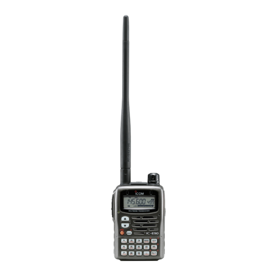
- Page 1 MULTIBAND FM TRANSCEIVER ie90...
- Page 2 INTRODUCTION This service manual describes the latest service information for the IC-E90 MULTIBAND FM TRANSCEIVER at the time of publication. MODEL VERSION SYMBOL Europe Europe-1 EUR-1 United Kingdom Italy Spain France To upgrade quality, all electrical or mechanical parts and inter- nal circuits are subject to change without notice or obligation.
-
Page 3: Table Of Contents
TABLE OF CONTENTS SECTION 1 SPECIFICATIONS SECTION 2 INSIDE VIEWS SECTION 3 DISASSEMBLY INSTRUCTIONS SECTION 4 CIRCUIT DESCRIPTION 4 - 1 RECEIVER CIRCUITS ....................4 - 1 4 - 2 TRANSMITTER CIRCUITS .................... 4 - 4 4 - 3 PLL CIRCUITS......................... 4 - 5 4 - 4 POWER SUPPLY CIRCUITS .................. - Page 4 SECTION 1 SPECIFICATIONS GENERAL • Frequency range (Unit: MHz) 50 MHz 145 MHz 440 MHz Receiving Version 430 – 440 50 – 52 0.495–999.990 430 – 434 50 – 51 435 – 438 144 – 148 50.000–52.000, 144.000–146.000, 430.000–440.000 – EUR-1 430 –...
- Page 5 : 8 Ω RECEIVER • AF output impedance • Receiver system : Double-conversion superheterodyne • Squelch sensitivity* (typical; Except sprious points) • Intermediate frequency : 1st 13.350 MHz (FM/AM) Frequency (MHz) 13.350 MHz (WFM) 0.495–1.625 – 450 kHz 1.3 µV 1.625–4.995 –...
- Page 6 SECTION 2 INSIDE VIEWS • LOGIC UNIT • LOGIC UNIT Top view Bottom view RESET IC Crystal oscillator for CPU clock (IC142: S-80928CNMC) (X1: CR-687, 6.7584 MHz, Q40: UN9215) EEPROM (IC1: M30220MA-114RP) (IC2: HN58X24128FPI, Q2: UN9115) AF regulator (Q201: 2SB1201, Q202: XP1501) +3 regulator (Q8: 2SB1132,...
- Page 7 • AF UNIT • AF UNIT • AF UNIT 1st AF amplifier Top view Bottom view Bottom view (Q205: 2SD2216) AF mute R3V regulator (Q251: 2SJ364) Q208: 2SA1576 Q209: XP1501 AF power amplifier AM/FM switch (IC252: TA7368F) (Q206: XP4315) AM detector (Q201, Q202: XP6501) FM IF IC (IC151: TA31136FN)
- Page 8 SECTION 3 DISASSEMBLY INSTRUCTIONS 1. Removing the rear panel 3. Removing the AF unit Vol lead Rear panel Vol plate Antenna plate AF unit J251 Rear panel Lock plate q Unscrew 1 screw A (M2 × 4 mm, black) q Take off the lock plate. w Unsolder 5 points F at the antenna plate, vol plate and w Unscrew 2 screws B (M2 ×...
-
Page 9: Circuit Description
SECTION 4 CIRCUIT DESCRIPTION 4-1 RECEIVER CIRCUITS • RF signals 0.495 MHz–75.995 MHz The signals pass through the antenna switching circuit (D9), 4-1-1 TRIPLEXER CIRCUIT (RF UNIT) and then applied to the RF circuit. The transceiver has a triplexer (low-pass and bandpass fil- ters) on the first stage from the antenna switching diode to •... - Page 10 The amplified or filtered RF signals are mixed with 1st LO (3) 76.0 MHz–229.995 MHz RF CIRCUIT signals at the 1st mixer (IC351) to produce a 69.45 MHz 1st The signals from the antenna switching circuit pass through IF signal. The 1st IF signal is output from pin 6, and passed the attenuator (D351), and then applied to the bandpass fil- through the bandpass filter (Narrow: AF unit;...
- Page 11 (1) AM DETECTOR CIRCUIT The AF filter circuit (LOGIC unit; IC241, pin 5) removes AF The filtered signals are applied to the AM detector circuit signals below 300 Hz (CTCSS signals) for clear AF output (Q201, Q202) to demodulate the 2nd IF signal into the AM AF and these are applied to the CPU (LOGIC unit;...
-
Page 12: Transmitter Circuits
4-1-8 AGC CIRCUIT (AF AND RF UNITS) The signal from the two LO amplifiers (VCO unit; Q16, Q212) is passed through the Transmit/Receive switch (Q51), and is The AGC (Automatic Gain Control) circuit reduce signal fad- amplified at the buffer amplifier (IC51, pin 1). The signal is ing and keeps the audio output level constant. -
Page 13: Pll Circuits
4-2-5 APC CIRCUIT (RF UNIT) 4-3 PLL CIRCUITS The APC circuit protects the power amplifier from a mis- 4-3-1 GENERAL matched output load and stabilizes the output power. The A PLL circuit provides stable oscillation of the transmit fre- APC circuit is designed to use VHF and UHF bands com- quency and the receive local frequency. - Page 14 • 430 MHz VCO CIRCUIT When the signal bypasses the divider circuit (IC1), it passes The oscillated signal at the 430 MHz VCO circuit (Q4, Q5, through the divider switch (D8, D10). D3) is amplified at two buffer amplifiers (Q7, Q11), and is then applied to the PLL IC (IC201, pin 19).
-
Page 15: Power Supply Circuits
4-4 POWER SUPPLY CIRCUITS 4-5 PORT ALLOCATIONS VOLTAGE LINE 4-5-1 D/A CONVERTOR IC (RF UNIT; IC251) DESCRIPTION LINE Port Description number name The voltage from the external power supply or Outputs frequnecy setting D/A data to attached battery pack. FSET the reference oscillator (RF unit;... - Page 16 4-5-3 CPU (LOGIC UNIT; IC1) Port Port Description Description number name number name Input port for the PA’s temperature Outputs the mic amplifier regulator PATMP MICC while transmitting. control signal. Input port for the S-meter signal. Input port for the SQL detection noise NOISE signal.
- Page 17 4-5-3 CPU (Continued) Port Description number name Outputs the 50 MHz modulation circuit control signal. Low: While 50 MHz is transmitting. Outputs the CT3 switch (LOGIC unit; CTSEL Q301) control signal. Low: DTCS/CTCSS is selected. Outputs the DTCS decorder filter con- DTCS trol signal.
-
Page 18: Adjustment Procedures
SECTION 5 ADJUSTMENT PROCEDURES 5-1 PREPARATION Some adjustments must be adjusted on the adjustment mode. When entering the adjustment mode, the 68 kΩ terminator (as shown at page 5-2) is required. ‘ ‘ REQUIRED TEST EQUIPMENT EQUIPMENT GRADE AND RANGE EQUIPMENT GRADE AND RANGE Output voltage... - Page 19 • CONNECTION Standard signal generator to the antenna connector 0.1 V to 32 mV to [MIC] Audio generator ( 127 dBm to 17 dBm) CAUTION: DO NOT transmit while an SSG is connected to the antenna connector. 68 k to [SP] jack Attenuator deviation meter 40 dB or 50 dB...
-
Page 20: Trimmer Adjustment
5-2 TRIMMER ADJUSTMENT The following adjustment must be performed on the normal mode. ADJUSTMENT MEASUREMENT POINT ADJUSTMENT ADJUSTMENT CONDITION VALUE UNIT LOCATION UNIT ADJUST PLL LOCK • Displayed frequency Connect 0.4 V–1.0 V Verify VOLTAGE : 30.000 MHz voltmeter • Mode : FM oscilloscope to the •... - Page 21 • VCO UNIT PLL lock voltage check point • RF UNIT L456 TX power balance adjustment (435 MHz) TX power balance adjustment (145 MHz) 5 - 4...
-
Page 22: Adjustment Mode Adjustments
5-3 ADJUSTMENT MODE ADJUSTMENTS The following adjustment must be performed at “ADJUSTMENT MODE”. ADJUSTMENT MEASUREMENT POINT ADJUSTMENT ADJUSTMENT CONDITION VALUE UNIT LOCATION UNIT ADJUST REFERENCE • Displayed frequency : Loosely couple the 445.0000 MHz [DIAL] FREQUENCY (Fr ch.) 445.000 MHz panel frequency counter panel... - Page 23 ADJUSTMENT MODE ADJUSTMENTS (Continued) • The following adjustment must be performed at “ADJUSTMENT MODE”. • The adjustment channel indicators (PL, DL, PH, DH, PE, DE) need to change from “DH” channel indicator to push “0” or “.” keys. ADJUSTMENT MEASUREMENT POINT ADJUSTMENT ADJUSTMENT CONDITION...
- Page 24 ADJUSTMENT MODE ADJUSTMENTS (Continued) • The following adjustment must be performed at “ADJUSTMENT MODE”. • The adjustment channel indicators (PL, DL, PH, DH, PE, DE) need to change from “DH” channel indicator to push “0” or “.” keys. ADJUSTMENT MEASUREMENT POINT ADJUSTMENT ADJUSTMENT CONDITION...
- Page 25 ADJUSTMENT MODE ADJUSTMENTS (Continued) • The following adjustment must be performed at “ADJUSTMENT MODE”. • The adjustment channel indicators (PL, DL, PH, DH, PE, DE) need to change from “DH” channel indicator to use “0” or “.” keys. ADJUSTMENT MEASUREMENT POINT ADJUSTMENT ADJUSTMENT CONDITION...
-
Page 26: Logic Unit
ADJUSTMENT MODE ADJUSTMENTS (Continued) • The following adjustment must be performed at “ADJUSTMENT MODE”. ADJUSTMENT MEASUREMENT POINT ADJUSTMENT ADJUSTMENT CONDITION VALUE UNIT LOCATION UNIT ADJUST • Displayed frequency : Connect ± 4.2 kHz LOGIC R365 DEVIATION (DH ch.) 53.900 MHz Panel deviation meter to (50 MHz) - Page 27 ADJUSTMENT MODE ADJUSTMENTS (Continued) • The following adjustment must be performed at “ADJUSTMENT MODE”. ADJUSTMENT MEASUREMENT POINT ADJUSTMENT ADJUSTMENT CONDITION VALUE UNIT LOCATION UNIT ADJUST CTCSS • Displayed frequency : Connect ± 0.55 kHz [DIAL] DEVIATION (CT ch.) 53.900 MHz Panel deviation meter to panel...
- Page 28 ADJUSTMENT MODE ADJUSTMENTS (Continued) The following adjustment must be performed at “ADJUSTMENT MODE”. “DETECTOR COIL” adjustment must be performed on same channel as “DTCS DEVIATION ADJUSTMENT” (DT ch.). ADJUSTMENT MEASUREMENT POINT ADJUSTMENT ADJUSTMENT CONDITION VALUE UNIT LOCATION UNIT ADJUST DETECTOR •...
-
Page 29: Af Unit / Vco Unit
NOTE: A: [EUR], [ITR], [UK] only B: except [ESP] • AF UNIT Detector coil check point IC151, pin 12 (SD line) RF Tracking check point L151 Detector coil adjustment 5 - 12... - Page 30 ADJUSTMENT MODE ADJUSTMENTS (Continued) The following adjustment must be performed at “ADJUSTMENT MODE”. ADJUSTMENT MEASUREMENT POINT ADJUSTMENT ADJUSTMENT CONDITION VALUE UNIT LOCATION UNIT ADJUST • Displayed frequency : Connect a DC volt- Maximum voltage [DIAL] TRACKING (TM ch.) 430.100 MHz meter oscillo panel...
- Page 31 ADJUSTMENT MODE ADJUSTMENTS (Continued) The following adjustment must be performed at “ADJUSTMENT MODE”. ADJUSTMENT ADJUSTMENT CONDITION OPERATION S-METER • Displayed frequency : Push the [BAND] key. (SM ch.) 1.620 MHz B • Mode : FM • Connect the SSG to the antenna connector and set as: Level : 0.63 µV (–111 dBm)
- Page 32 SECTION 6 PARTS LIST [RF UNIT] [RF UNIT] ORDER ORDER DESCRIPTION DESCRIPTION IC51 1110005590 S.IC µPC2762TB-E3 D405 1720000790 S.VARICAP HVC321B1TRF IC101 1110004050 S.IC NJM3404AV-TE1 D406 1790001260 S.DIODE MA2S077-(TX) IC251 1110004530 S.IC M62368GP 70ED D407 1720000790 S.VARICAP HVC321B1TRF IC351 1110005230 S.IC µPC2757TB-E3 D408 1750000800 S.DIODE...
- Page 33 [RF UNIT] [RF UNIT] ORDER ORDER DESCRIPTION DESCRIPTION L452 6200005610 S.COIL ELJRE 3N9Z-F R361 7030007290 S.RESISTOR ERJ2GEJ 222 X (2.2 kΩ) L453 6200005610 S.COIL ELJRE 3N9Z-F R362 7030007300 S.RESISTOR ERJ2GEJ 332 X (3.3 kΩ) L454 6200006980 S.COIL ELJRE R10G-F R363 7030007570 S.RESISTOR ERJ2GEJ 122X (1.2 kΩ) L455...
- Page 34 [RF UNIT] [RF UNIT] ORDER ORDER DESCRIPTION DESCRIPTION 4030017510 S.CERAMIC ECJ0EC1H680J C354 4030017460 S.CERAMIC ECJ0EB1E102K 4030016790 S.CERAMIC ECJ0EB1C103K C355 4030017460 S.CERAMIC ECJ0EB1E102K 4030017330 S.CERAMIC ECJ0EF1C104Z C356 4030017460 S.CERAMIC ECJ0EB1E102K 4030017640 S.CERAMIC ECJ0EC1H150J C357 4030017460 S.CERAMIC ECJ0EB1E102K 4030017460 S.CERAMIC ECJ0EB1E102K C358 4030017460 S.CERAMIC ECJ0EB1E102K 4030016790 S.CERAMIC...
- Page 35 [RF UNIT] [AF UNIT] ORDER ORDER DESCRIPTION DESCRIPTION J251 6510022860 S.CONNECTOR AXK6S30445P 6050010160 S.XTAL CR-583 (13.800 MHz) J252 6450000870 CONNECTOR HEC2711-01-020 6200004600 S.COIL MLF1608D R15K-T 7030010040 S.JUMPER ERJ2GE-JPW 6200004590 S.COIL MLF1608D R18K-T 7030010040 S.JUMPER ERJ2GE-JPW 6200004590 S.COIL MLF1608D R18K-T 6200005700 S.COIL ELJRE 22NG-F 6200004600 S.COIL MLF1608D R15K-T...
- Page 36 [AF UNIT] [AF UNIT] ORDER ORDER DESCRIPTION DESCRIPTION R216 7030008290 S.RESISTOR ERJ2GEJ 183 X (18 kΩ) C157 4030017460 S.CERAMIC ECJ0EB1E102K R217 7030008290 S.RESISTOR ERJ2GEJ 183 X (18 kΩ) C158 4030017460 S.CERAMIC ECJ0EB1E102K R218 7030005050 S.RESISTOR ERJ2GEJ 103 X (10 kΩ) C159 4030017330 S.CERAMIC ECJ0EF1C104Z...
- Page 37 [AF UNIT] [LOGIC UNIT] ORDER ORDER DESCRIPTION DESCRIPTION J252 6450001680 CONNECTOR HSJ1122-010010 1790001250 S.DIODE MA2S111-(TX) J253 6450002250 CONNECTOR HSJ1456-010320 [EUR-1], [ESP], [FRA] only 1790001250 S.DIODE MA2S111-(TX) 1790001250 S.DIODE MA2S111-(TX) [EUR-1], [ESP] only S251 7600000210 ENCODER TP70N00E20-15F-1903 1790001200 S.DIODE MA6S121 (TX) 1790001560 S.DIODE 1SS372 (TE85R) D141...
- Page 38 [LOGIC UNIT] [LOGIC UNIT] ORDER ORDER DESCRIPTION DESCRIPTION 7030005050 S.RESISTOR ERJ2GEJ 103 X (10 kΩ) R456 7030005240 S.RESISTOR ERJ2GEJ 473 X (47 kΩ) 7030005050 S.RESISTOR ERJ2GEJ 103 X (10 kΩ) R457 7030005110 S.RESISTOR ERJ2GEJ 224 X (220 kΩ) 7030005240 S.RESISTOR ERJ2GEJ 473 X (47 kΩ) R458 7030005240 S.RESISTOR...
-
Page 39: Vco Unit
[LOGIC UNIT] [LOGIC UNIT] ORDER ORDER DESCRIPTION DESCRIPTION C198 4030017460 S.CERAMIC ECJ0EB1E102K 8900010520 CABLE OPC-1033 C199 4030017460 S.CERAMIC ECJ0EB1E102K 7120000470 JUMPER ERDS2T0 C200 4030017460 S.CERAMIC ECJ0EB1E102K 7030000010 S.JUMPER MCR10EZHJ JPW (000) C205 4550006210 S.TANTALUM ECST1CX106R C207 4030011810 S.CERAMIC C1608 JB 1A 224K-T C208 4030017460 S.CERAMIC ECJ0EB1E102K... - Page 40 [VCO UNIT] [VCO UNIT] ORDER ORDER DESCRIPTION DESCRIPTION 7030005040 S.RESISTOR ERJ2GEJ 472 X (4.7 kΩ) C228 4030017420 S.CERAMIC ECJ0EC1H470J 7030007570 S.RESISTOR ERJ2GEJ 122X (1.2 kΩ) C229 4030017420 S.CERAMIC ECJ0EC1H470J 7030005040 S.RESISTOR ERJ2GEJ 472 X (4.7 kΩ) C230 4030017460 S.CERAMIC ECJ0EB1E102K ERJ2GEJ 221 X (220 Ω) 7030004990 S.RESISTOR C232...
- Page 41 SECTION 7 MECHANICAL PARTS AND DISASSEMBLY [CHASSIS PARTS] [AF UNIT] ORDER ORDER QTY. QTY. DESCRIPTION DESCRIPTION 6510022671 Connector SMA-R235-1 S251 7600000210 Encoder TP70N00E20-15F-1903 8210018240 Panel 2507 REAR PANEL 63-222 8930058200 2507 A-AF sheet 8930054200 2372 Jack cap 8510014850 2507 AF shield 8930056321 2507 DC cap-1 8310050390...
- Page 42 MP3 (L) MP14 (L) EP1 (L) MP13 (L) DS4 (L) MP15 (L) MP13 (L) MP7 (L) MP5 (C) MP2 (C) MP10 (L) MP9 (L) MP22 (C) MP11 (C) MP1 (L) MP19 (C) MP12 (C) MP4 (L) MP1 (C) MP25 (C) MP6 (L) MP5 (L) SP1 (L)
- Page 43 SECTION SECTION 8 PARTS LIST SEMI-CONDUCTOR INFORMATION 8 - 1 TRANSISTORS AND FETS 8 - 2 DIODES NAME SYMBOL INSIDE VIEW NAME SYMBOL INSIDE VIEW NAME SYMBOL INSIDE VIEW NAME SYMBOL INSIDE VIEW 2SA1576 S 1SS362 2SA1588-GR 2SK3475 XP4214 1SS372 2SB1462-R MA133 2SK3476...
- Page 44 The combination of this page and the next page SECTION 9 BOARD LAYOUTS shows the unit layout in the same configuration as the actual P.C. Board. 9 - 1 LOGIC UNIT MICROPHONE • TOP VIEW 9 - 1...
- Page 45 LOGIC unit The combination of this page and the previous • BOTTOM VIEW page shows the unit layout in the same configuration as the actual P.C. Board. W2 (L) W2 (L) to AF unit J251 9 - 2...
- Page 46 9 - 2 RF UNIT The combination of this page and the next page • TOP VIEW shows the unit layout in the same configuration as the actual P.C. Board. Antenna to VCO unit VSHFT VMOD +10V PDA/UL PLSTB to VCO unit to AF unit PDA/UL VMOD...
- Page 47 RF unit The combination of this page and the previous • BOTTOM VIEW page shows the unit layout in the same configuration as the actual P.C. Board. 9 - 4...
- Page 48 9 - 3 AF UNIT The combination of this page and the next page • TOP VIEW shows the unit layout in the same configuration as the actual P.C. Board. EXT.SP EXT.MIC REMOTO J252 J253 to S251 VCO UNIT • TOP VIEW to RF UNIT to RF UNIT VSFT...
- Page 49 The combination of this page and the previous page shows the unit layout in the same configuration as the actual P.C. Board. AF unit • BOTTOM VIEW S253 S252 VCO UNIT S251 • BOTTOM VIEW to RF unit J251 PDA/UL DATA VMOD PLSTB...
-
Page 50: Block Diagram
SECTION 10 BLOCK DIAGRAM LOGIC UNIT INTSP INTSP INTSP EXTM EXTM Q310: XP6501 Q310: XP6501 Q307: UN9214 Q304, Q305, Q342, Q343: 2SJ364 MICIN VMOD VMOD MUTE CHANGE Q311: XP5601 BEEP BEEP Q312: XP6501 MUTE MUTE IC5: TC4W53FU Q45: 2SC4116 XMOD XMOD XMOD CT/DT... - Page 51 D51: HVC136 D6: 1SV308 IC51: µPC2762TB Q7: 2SC5195 D7, D8: HVC136 D9, D10: HVC136 Q16: 2SC5008 Q212: 2SC5008 D54: HVC132 Q54: 2SC5289 D201: HVC136 Q51: 2SK3476 50–54 MHZ 0.495–75.995 MHz 430 MHz D9: 1SV308 50 MHz VMOD VMOD TX/RX BUFF BUFF DRIVE MUTE...
- Page 52 SECTION 11 VOLTAGE DIAGRAM 11 - 1 LOGIC UNIT REMO TTR5169 UPFDHW 1 2 3 4 5 6 7 8 9 10 11 12 13 14 15 16 17 18 19 20 21 22 23 24 25 26 27 28 29 30 31 32 33 34 35 36 37 38 39 40 +3CPU +3CPU CPUHV...
- Page 53 LOGIC UNIT 0.001 0.001 0.001 0.001 PATMP PATMP PATMP PATMP VMOD VMOD 0.01 XMOD XMOD DETO DETO 3.05V VOLC VOLC VOLC +3CPU +3CPU R152 MUTE MUTE BEEP BEEP BEEP EXTM CPUHV NOISE NOISE NOISE Q151 3.10V C103 R151 VSFT VSFT VSFT R153 0.001...
- Page 54 11 - 2 RF UNIT R5 1.8k R8 15 R240 C238 0.001 0.001 R471 1.5p 82nH 2.3V VCO3 VCO3 0.001 C226 C5 2p 0.001 EP2 MMZ1608D121B 10nH 0.82µH 12nH CP11 0.001 HVC321BTRF 5.6k 0.82µH 24nH 0.82µH 2SC5008 0.01 0.01 0.01 C224 C225 0.01...
- Page 55 11 - 3 AF UNIT TX: 0 RX: 2.9V UN9115 2SB1132 0.01 0.15µH TX: 6.02V RX: 0V 1SS364 1SS364 XP1115 15 16 TX: 0V RX: 0.63V XP1115 XP4214 2SA1588 22nH TX: 6.05V RX: 0V XP1501 0.18µH 0.18µH FSET 4.7k C301 XP1115 0.001 R266...
- Page 57 S-13903MZ-C2 1-1-32, Kamiminami, Hirano-ku, Osaka 547-0003, Japan 2002 Icom Inc.
Need help?
Do you have a question about the IC-E90 and is the answer not in the manual?
Questions and answers