
Related Manuals for Mitsubishi LCD1855NX-BK


Summary of Contents for Mitsubishi LCD1855NX-BK
-
Page 1: Color Monitor
COLOR MONITOR SERVICE MANUAL CHASSIS NO. : CL-29 FACTORY MODEL: LN801H ID LABEL MODEL No: L182ET MODEL: RDT181V(BK), NX85LCD LCD1855NX-BK CAUTION BEFORE SERVICING THE UNIT, READ THE SAFETY PRECAUTIONS IN THIS MANUAL. -
Page 2: Table Of Contents
CONTENTS SPECIFICATIONS ........... 2 ADJUSTMENT ............12 SERIAL NUMBER INFORMATION ......4 INSPECTION............17 PRECAUTIONS ............5 TROUBLESHOOTING GUIDE ......22 TIMING CHART ............6 PRINTED CIRCUIT BOARD........27 OPERATING INSTRUCTIONS ........ 7 EXPLODED VIEW...........30 WIRING DIAGRAM ..........8 REPLACEMENT PARTS LIST .......32 BLOCK DIAGRAM ........... -
Page 3: Signal Connector Pin Assignment
Signal Connector Pin Assignment • DVI-D Connector (Digital) Signal (DVI-D) Signal (DVI-D) T. M. D. S. Data2- Hot Plug Detect T. M. D. S. Data2+ T. M. D. S. Data0- T. M. D. S. Data2/4 Shield T. M. D. S. Data0+ T. -
Page 4: Serial Number Information
SERIAL NUMBER INFORMATION 206100001 Overprinting : Y MM C SSSSS (1) : Year code of Production(Last Number of year) ex)2000 0, 2001 1, 2002 (2) : Month code of Production Month 1 2 3 6 7 8 9 10 11 12 Number 01 02 03 04 05 06 07 08 09 10 11 12 (3) : Classification code... -
Page 5: Precautions
PRECAUTION WARNING FOR THE SAFETY-RELATED COMPONENT. WARNING BE CAREFUL ELECTRIC SHOCK ! • There are some special components used in LCD monitor that are important for safety. These parts are • If you want to replace with the new backlight (CCFL) or marked on the schematic diagram and the inverter circuit, must disconnect the AC adapter... -
Page 6: Timing Chart
TIMING CHART VIDEO SYNC << Dot Clock (MHz), Horizontal Frequency (kHz), Vertical Frequency (Hz), Horizontal etc... (µs), Vertical etc... (ms) >> Total Period Video Active Time Back Porch Sync Duration Front Portch Sync Mode Resolution Frequency Clock Polarity Sort 31.469 720x350 28.324 70Hz... -
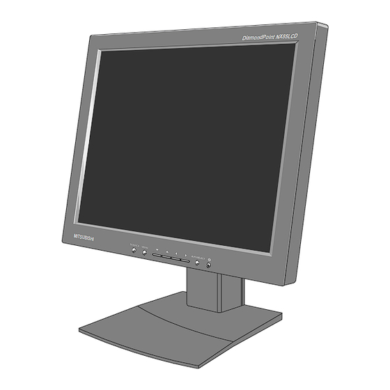
Page 7: Operating Instructions
FRONT VIEW REAR VIEW Power Connect Front Control Panel D-Sub Signal DVI Connect Connect Front Control Panel 1. Power ON/OFF Button Button Use this button to turn the monitor on or off. Use these buttons to choose or adjust items in the On Screen Display. -
Page 8: Wiring Diagram
Connector Ass’y P/N: 6631T25008Q MAIN PCB Connector Ass’y P/N: 6631T20015R P902 J705 MATAL FRAME J801 J702 J710 Connector Ass’y P/N: 6631T20008U CN_C02 CN_C01 CN301 MODULE Connector Ass’y P/N: 6631T11012P... -
Page 9: Block Diagram
LCD Module R,G,B differential Micom Memory 3.3 VM LVDS 68HC08-BD48 (KM416S102BT) Inverter (LVD S823) M-CLK Data 48 Bit Address Out - CLK H/V Sync DE ,H/V Sync out R,G,B /Odd 2.5V 3.3V 3.3V Gm5020 AVD D3.3V Reg. Reg. Reg. including AVD D2.5V (ADC / TMDS Rx ) H/V-S ync... -
Page 10: Description Of Block Diagram
DESCRIPTION OF BLOCK DIAGRAM 1. Video Controller Part(GM5020). This part amplifies the level of video signal for the anolog to digital conversion and converts from the analog video signal to the digital video signal using a pixelclock. The pixel clock for each mode is generated by the PLL. The range of the pixel clock is from 25MHz to 135MHz. - Page 11 50 ~ 60Hz 100KHz HVDC INPUT RECTIFIER ENERGY OUTPUT RECTIFIER COMPONENTS AND FILTER TRANSFER AND FILTER LINE 100 ~ 240V PWM CONTROL PHOTO-COUPLER SIGNAL CIRCUIT ISOLATION COLLECTION SECONDA RY PRIMARY Operation description_Power 1. EMI components. This part contains of EMI components to comply with global marketing EMI standards like FCC, VCCI CISPR, the circuit included a line-filter, across line capacitor and of course the primary protection fuse.
-
Page 12: Adjustment
ADJUSTMENT 1. Application This specification shall be applied to the adjustment and inspection of the LN801H. 2. Adjustment Setup All adjustment are thoroughly checked and corrected when the monitor leaves the factory, but sometimes several minor adjustment may be required. Adjustment should be following procedure and after more than 30 minutes. - Page 13 3. Adjustment 3-1. Initialization and Aging Prior to adjustment of this model, more than 30 minutes of aging shall be carried out. 1) Display any pattern at any Mode. 2) Run adjustment program for LN801H on the IBM compatible PC. <<...
- Page 14 3-2. Adjustment of Factory Preset Mode. 1) It’s not necessary for preset mode adjustment. All preset mode data shall be written to EEPROM at initial power on. 2) IMPORTANT At the initial Power turn on, maintain power on status more than 3 seconds. 3-3.
- Page 15 8) Select PRESET EXIT command and Enter. << LCD IIC ADJUST. PROGRAM :LCD185~1. DAT >> DIST. ADJ COLOR ADJ COMMAND EDIT EEPROM QUIT PRESET START PRESET EXIT MENU Move : Arrow or Space MENU Select : Enter Quit : ESC 3-4.
- Page 16 * How to change the EDID (Serial No. etc.) 1. Operate adjustment Program 2. Select EDID INFO of the EDID Menu for Analog EDID and DDC INFO for Digital EDID. 3. First. You can see the blank screen, and press "Enter" key and you can see the EDID Contents 4.
-
Page 17: Inspection
INSPECTION 1. PERFORMANCE INSPECTION ITEMS PATTERN INSPECTION CRITERIA 200(min.) , 250(typ.) Check Luminance on 255 g rey level Luminance Full White Cd/m2 at the center 1) Measure luminance at each point (5 point) on brightness/contrast max condition. 2) Calculate l/u with formula. Luminance Full White 75 % (max.) - Page 18 2. COSMETIC INSPECTION 1.1 DO T DEFECT This criteria is based on ISO-13406-2 Pixel Faults Class II Items Criteria Remarks 1) Bright Dots Horizontally adjacent 2 dots (R+G, G+B) Max. 3 Note 1 2) Dark Dots Max. 3 Note 2 Adjacent Dots Horizontally, vertically or combined adjacent 3 dots 3) Bright Dots...
- Page 19 Note 2. 1) + 2) : Max. 3 Note 3. Horizontally, vertically or combined adjacent 3 dots ( separately bright dots and dark dots) Count as adjacent 3 dots Do not count as adjacent 3 dots Note 4. Do not count the horizontally adjacent 2 dots (R-G, G-B) Note 5.
- Page 20 Note 7. Two or more pixels or sub-pixels with more than one fault of 5) within 5x5 pixels 5x5 pixels Dot Defect (5) 1 Cluster The number of cluster within all screen : Max. 3 Note 8. Two or more pixels or sub-pixels with more than one fault of 1) or 2) within 5x5 pixels Count as defect Do not count as defect 5x5 pixels...
- Page 21 1.3 Foreign Material Items Criteria 0.03 0.152, (Bright), Linear 0.03 0.10(Dark), Foreign 3.0, N Material 1.0(White/Dark), Circular 1.3(Gray), N W : Width L : Length D : Average diameter Note a. Average Diameter b. Linear : a 2b , Circular : a 1.4 Line Defect All kinds of line defects such as vertical, horizontal or cross are not allowed.
-
Page 22: Troubleshooting Guide
TROUBLESHOOTING GUIDE 1. NO POWER NO POWER (POWER INDICATOR OFF) CHECK J801 TROUBLE IN INPUT VOLTAGE BULT-IN POWER (12V) ? CHECK J801 TROUBLE IN 5VST VOLTAGE BULT-IN POWER (5V) ? CHECK U501’s PIN 6. TROUBLE IN IS THIS PIN U501 or X501 OSCILLATED? TROUBLE SOMEWHERE ELSE... - Page 23 2. NO RASTER NO RASTER CHECK TROUBLE IN J702 PIN 1, 2, 3 POWER ADATER (12V) ? or L703, L704 CHECK TROUBLE IN J702 PIN 8 (5V) ? INVON PATTERN CHECK TROUBLE IN X501 X501 H. PULSE ? CHECK TROUBLE IN U201(GM5020) ? U201 CHECK...
- Page 24 CHECK TROUBLE IN L204 U201 PULSE ? CHECK CHECK DOT CLOCK U401 PIN 10 PATTERN PULSE ? CHECK CHECK U401 PIN 8 V.PULSE? DVS PATTERN CHECK CHECK U401 PIN 7 DHS PATTERN V.PULSE? TROUBLE IN LCD MODULE - 24 -...
- Page 25 3. NO CLOCK (CLOCK GENERATOR) NO DOT CLOCK CHECK TROUBLE IN X201 24MHz ? X201 CHECK TROUBLE IN L201 U201 CLOCK ? - 25 -...
- Page 26 4. TROUBLE IN DPM TROUBLE IN DPM CHECK PC CHECK PC IS NOT GOING R233, R234? INTO DPM OFF MODE CHECK U501 PIN 6 TROUBLE IN WAVEFORM X501 (24MHz) ? CHECK TROUBLE IN U501 PIN 11 SIGNAL CABLE (0V) ? TROUBLE IN PC - 26 -...
-
Page 27: Printed Circuit Board
9 10 11 12 13 14 15 16 17 18 19... - Page 28 C861 R540 R523 R528 R529 C740 R830 R522 R828 C511 C530 R541 R829 R820 R819 R811 C510 R519 C710 R812 R518 R818 R817 R813 R516 R816 R814 C513 C520 R827 R534 R815 C833 R538 R535 R831 R531 R826 R536 C832 R505 R539 R580...
- Page 29 3. POWER BOARD (Component Side) 4. POWER BOARD (Solder Side) 5. CONTROL BOARD...
- Page 31 Ref. No. Part No. CABINET ASSEMBLY, LN801H NMV 3090TKL045 BK-EP94(JAPAN) -RDT181V(BK) 3091TKL044E CABINET ASSEMBLY, LN801H NMV 3090TKL045A -EP94(BLACK)NEC-NORTH AMERICA-LCD1855NX-BK 3091TKL044F CABINET ASSEMBLY, LN801H NMV 3090TKL045A EP94(BLACK)Mitsubishi-NORTH AMERICA- NX85LCD 3091TKL044C LCD(LIQUID CRYSTAL DISPLAY), LM181E06-A4M1 LG PHILPS TFT COLOR SXGA 18.1" LVDS SMM...
-
Page 32: Replacement Parts List
REPLACEMENT PARTS LIST CAUTION: BEFORE REPLACING ANY OF THESE COMPONENTS, READ CAREFULLY THE SAFETY PRECAUTIONS IN THIS MANUAL. * NOTE SAFETY Mark AL ALTERNATIVE PARTS DATE: 2002. 07. 02. DATE: 2002. 07. 02. *S *AL LOC. NO. PART NO. DESCRIPTION / SPECIFICATION *S *AL LOC. - Page 33 DATE: 2002. 07. 02. DATE: 2002. 07. 02. *S *AL LOC. NO. PART NO. DESCRIPTION / SPECIFICATION *S *AL LOC. NO. PART NO. DESCRIPTION / SPECIFICATION C517 0CC101CK41A 100PF 1608 50V 5% R/TP NP0 D702 0DS226009AA KDS226 TP KEC SOT-23 80V 300MA C519 0CC101CK41A 100PF 1608 50V 5% R/TP NP0...
- Page 34 DATE: 2002. 07. 02. DATE: 2002. 07. 02. *S *AL LOC. NO. PART NO. DESCRIPTION / SPECIFICATION *S *AL LOC. NO. PART NO. DESCRIPTION / SPECIFICATION L703 6210TCE001G HH-1M3216-501 CERATEC 3216MM R/ R406 0RJ0000D677 0 OHM 1/10 W 5% 1608 R/TP L704 6210TCE001G HH-1M3216-501 CERATEC 3216MM R/...
- Page 35 DATE: 2002. 07. 02. DATE: 2002. 07. 02. *S *AL LOC. NO. PART NO. DESCRIPTION / SPECIFICATION *S *AL LOC. NO. PART NO. DESCRIPTION / SPECIFICATION R729 0RJ4700D677 470 OHM 1/10 W 5% 1608 R/TP RA242 0RHZTCZ001A 100 OHM 1/16 W 5% 3215 R/TP CHI R730 0RJ5600D677 560 OHM 1/10 W 5% 1608 R/TP...
- Page 36 DATE: 2002. 07. 02. *S *AL LOC. NO. PART NO. DESCRIPTION / SPECIFICATION R913 0RN1102F409 11K 1/6W 1% TA52 R914 0RD1002Q609 10K 1/4W(3 5% TA52 R917 0RD1201Q609 1.20K 1/4W(3 5% TA52 R918 0RD1000Q609 100 1/4W(3 5% TA52 R920 0RN4702F409 47K 1/6W 1% TA52 R921 0RN2701F409 2.70K 1/6W 1% TA52...
-
Page 37: Pin Configuration
PIN CONFIGURATION GM5020 GENESIS 292P FUNCTIONAL BLOCK DIAGRAM Serial I/F SDRAM/I/F Host Micro- Frame Store Interface processor Interface Anolog Triple YUV to RGB Output Converter Image Panel I/F Digital Zoom/ Data Frame Rate TMDS Caputure/ [48-bits] Gamma TMDS Brightness, Shrink/ Path/ Conversion Measure. - Page 38 CAT24WC08J-TE13 8P BLOCK DIAGRAM DIP Package(p) SOIX Package(J) EXTERNAL LOAD V CC V CC SENSE AMPS D OUT SHIFT REGISTERS V SS V SS V CC COLUMN V SS WORD ADDRESS DECODERS BUFFERS TSSOP Package(U) START/STOP LOGIC V CC E PROM XDEC V SS CONTROL...
Need help?
Do you have a question about the LCD1855NX-BK and is the answer not in the manual?
Questions and answers