Table of Contents
Advertisement
SERVICE MANUAL
Ver 1.1 2004.02
CX-BK7 is the amplifier, disc player, tape
deck and tuner section in BMZ-K7D.
This system incorporates Dolby* Digital, Dolby Pro
Logic (II) adaptive matrix surround decoder, and the
DTS** Digital Surround System.
* Manufactured under license from Dolby
Laboratories.
"Dolby", "Pro Logic" and the double-D symbol are
trademarks of Dolby Laboratories.
** Manufactured under license from Digital Theater
Systems, Inc. "DTS" and "DTS Digital Surround"
are registered trademarks of Digital Theater
Systems, Inc.
US and foreign patents licensed from Dolby
Laboratories.
Amplifie r section
The following measured at AC 120, 127, 220, 240 V,
50/60 Hz
Rated Power Output at Stereo mode
Continuous RMS power output (reference)
Front speaker:
150 + 150 watts
(6 ohms at 1 kHz, 10%
THD)
Center speaker:
50 watts (8 ohms at 1 kHz,
10% THD)
Surround speaker:
50 watts (8 ohms at 1 kHz,
10% THD)
Inputs
LINE IN AUDIO (phono jacks):
voltage 1.1V, impedance
47 kilohms
LINE IN VIDEO (phono jack):
max. input level 1Vp-p,
unbalanced, Sync
negative, impedance
75 ohms
MD (AUX) IN (phono jacks):
voltage 1.1V, impedance
47 kilohms
MIC (phone jack):
sensitivity 1 mV,
impedance 10 kilohms
Sony Corporation
9-961-333-02
2004B05-1
Home Audio Company
C 2004.02
Published by Sony Engineering Corporation
Model Name Using Similar Mechanism
DVD
DVD Mechanism Type
Section
Optical Traverse Unit Name
Model Name Using Similar Mechanism
Tape deck
Section
Tape Transport Mechanism Type
SPECIFICATIONS
Outputs
MD (AUX) OUT (phono jacks):
voltage 500 mV,
impedance 4.7 kilohms
VIDEO OUT (phono jack):
max. output level
1 Vp-p, unbalanced, Sync
negative, load impedance
75 ohms
S-VIDEO OUT (4-pin/mini-DIN jack):
Y: 1 Vp-p, unbalanced,
Sync negative,
C: 0.286 Vp-p, load
impedance 75 ohms
COMPONENT VIDEO OUT:
Y: 1 Vp-p, 75 ohms
P
, P
: 0.7 Vp-p, 75 ohms
B
R
PHONES (stereo mini jack):
accepts headphones of
32 ohms or more
Front speaker:
Use only the supplied
speaker SX-BK7
Surround speaker:
Use only the supplied
speaker SX-BK7R
Center speaker:
Use only the supplied
speaker SX-BK7C
SUB WOOFER OUT:
voltage 1 V,
impedance 1 kilohm
CX-BK7
AEP Model
UK Model
E Model
Australian Model
NEW
CDM69DV-DVBU16V
DBU-1
NEW
CMAL1Z241A
Disc player section
System
Compact disc and digital
audio and video system
Laser
Semiconductor laser
(DVD: =657 nm,
CD: =793 nm)
Emission duration:
continuous
Frequency response
DVD (PCM 48 kHz):
2 Hz 22 kHz ( 1 dB)
CD: 2 Hz 20 kHz ( 1 dB)
Video color system format
NTSC, PAL
OPTICAL DIGITAL OUT (Euro/UK, Russian models
only)
(Square optical connector jack, rear panel)
Wavelength
660 nm
Tape deck section
Recording system
4-track 2-channel stereo
Frequency response
100 10,000 Hz ( 3 dB),
using Sony TYPE I cassette
– Continued on next page –
DVD DECK RECEIVER
Advertisement
Table of Contents

Related Manuals for Aiwa CX-BK7


Summary of Contents for Aiwa CX-BK7
-
Page 1: Service Manual
UK Model Ver 1.1 2004.02 E Model Australian Model CX-BK7 is the amplifier, disc player, tape deck and tuner section in BMZ-K7D. This system incorporates Dolby* Digital, Dolby Pro Model Name Using Similar Mechanism Logic (II) adaptive matrix surround decoder, and the DTS** Digital Surround System. - Page 2 It is best to use only unleaded solder but unleaded solder may AND IN THE PARTS LIST ARE CRITICAL TO SAFE also be added to ordinary solder. OPERATION. REPLACE THESE COMPONENTS WITH SONY PARTS WHOSE PART NUMBERS APPEAR AS SHOWN IN THIS MANUAL OR IN SUPPLEMENTS PUB- LISHED BY SONY.
-
Page 3: Playable Discs
DVD is prohibited by For Joliet in the expansion format (file and folder area restrictions. names can have up to 64 characters) make sure of the contents of the writing software, etc. MODEL NO. CX-BK7 DVD DECK RECEIVER AC:230V 50/60Hz Region code Multi Session SERIAL NO.AREA... -
Page 4: Session
CX-BK7 Notes on discs Note on playback operations Cautions when playing a disc of DVDs and VIDEO CDs that is recorded in Multi • This system can play CD-R/CD-RW discs Session edited by the user. However, note that Some playback operations of DVDs and VIDEO... -
Page 5: Table Of Contents
CX-BK7 TABLE OF CONTENTS 7-17. Schematic Diagram – MB03 Board (5/8) – ....54 SERVICING NOTES ..........6 7-18. Schematic Diagram – MB03 Board (6/8) – ....55 7-19. Schematic Diagram – MB03 Board (7/8) – ....56 GENERAL ..............8 7-20. -
Page 6: Servicing Notes
CX-BK7 SECTION 1 SERVICING NOTES • MODEL IDENTIFICATION NOTES ON HANDLING THE OPTICAL PICK-UP – Rear Cover – BLOCK OR BASE UNIT The laser diode in the optical pick-up block may suffer electro- static break-down because of the potential difference generated by the charged electrostatic load, etc. - Page 7 CX-BK7 – DVD mechanism deck – • In checking the DVD mechanism deck section, prepare two extension jigs (Part No. J-2501-103-A: 1mm Pitch, 29 cores, Length 300mm/Part No. J-2501-248-A: 1mm Pitch, 27 cores, Length 300mm). Note: The DVD mechanism deck of this model is a vertical type and putting it vertically as shown in the figure is the standard position.
-
Page 8: General
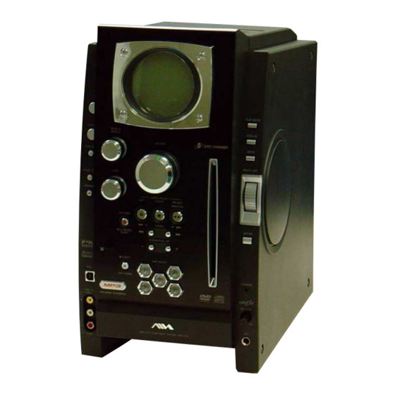
CX-BK7 SECTION 2 This section is extracted from instruction manual. GENERAL • LOCATION OF CONTROLS Main unit 1 Display window BUTTON DESCRIPTIONS 2 VOLUME control [/1 (power) wl 3 PLAY MODE X (pause) ws 4 DISPLAY Z (eject) qk 4 RDS... -
Page 9: Disassembly
CX-BK7 SECTION 3 DISASSEMBLY • This set can be disassembled in the order shown below. 3-1. DISASSEMBLY FLOW Note 1: The process described in can be performed in any order. Note 2: Without completing the process described in , the next process can not be performed. -
Page 10: Panel
CX-BK7 Note: Follow the disassembly procedure in the numerical order given. 3-2. PANEL 1 three screws (BVTP3 × 10) 6 three screws (BVTP3 × 10) 3 four claws 2 four screws (BVTP3 × 10) 0 right panel 5 panel (left) -
Page 11: Front Panel Assy
CX-BK7 3-4. FRONT PANEL ASSY 3 wire (flat type) (5core) (CN503) 2 wire (flat type) (17core) (CN004) 1 wire (flat type) (19core) (CN905) q; front panel assy 4 two lead with connectors 6 two screws 8 two claws (QT2+3-10) 9 connector (CN530) -
Page 12: Main Board
CX-BK7 3-6. MAIN BOARD 9 two connectors 2 wire (flat type) (CN007, CN507) (11core: EXCEPT AEP, UK) (CN509) (15core: AEP, UK) (CN508) 1 wire (flat type) (11core) (CN502) 6 wire (flat type) (11core) (CN501) 7 connector qf main board 3 two screws (CN007) (BVTP3 ×... -
Page 13: Tuner (Fm/Am)
CX-BK7 3-8. TUNER (FM/AM) 1 two screws (BVTP3 × 8) 2 tuner (FM/AM) 3-9. SP BOARD 1 two screws (BVTP3 × 12) 2 condenser cover 6 seven screws (BVTP3 × 10) 3 lead with connector 4 wire (flat type) (15core) -
Page 14: Acdc Board, Power Transformer
CX-BK7 3-10. ACDC BOARD, POWER TRANSFORMER 1 two connectors 4 two screws (CN003, CN005) (BVTP3 × 10) 2 connector (CN006) 6 ACDC board 5 five screws (BVTP3 × 10) 3 connector (CN011) 7 connector (CN014) 8 connector (CN008) 9 four screws... -
Page 15: Dvd Mechanism Deck (Cdm69Dv-Dvbu16V)
CX-BK7 3-12. DVD MECHANISM DECK (CDM69DV-DVBU16V) 1 four screws 5 mecanical holder (disk) (BVTP3 × 10) 4 four screws (BVTP3 × 10) 6 DVD mechanism deck 2 four screws (BVTP3 × 10) (CDM69DV-DVBU16V) 3 mechanical cover (disk) 3-13. SIGNAL CASSETTE MECHANISM 8 shield plate (top) 5 five screws (BVTP3 ×... -
Page 16: Optical Pick-Up Section (Dvbu16V)
CX-BK7 3-14. OPTICAL PICK-UP SECTION (DVBU16V) 3 boss 1 screw (PTPWHM2.6) 5 boss 4 boss 6 optical pick-up section (DVBU16V) 3-15. OPTICAL TRAVERSE UNIT (SERVICE ASSY, DBU-1) 1 step screw (M) 2 step screw (M) 8 insulator qa optical traverse unit... -
Page 17: Sw (1) Board, Sw (2) Board, Sw (3) Board, Sw (4) Board, Bracket (Top) Assy
CX-BK7 3-16. SW (1) BOARD, SW (2) BOARD, SW (3) BOARD, SW (4) BOARD, BRACKET (TOP) ASSY 4 SW (3) board 5 SW (4) board 3 SW (2) board 1 four screws (BTP2.6 × 6) 6 six screws (BVTP2.6 × 8) -
Page 18: Motor (Stocker) Assy (Stocker) (M761)
CX-BK7 3-18. MOTOR (STOCKER) ASSY (STOCKER) (M761) 3 two screws (BVTP2.6 × 8) 2 Remove two solders. 5 stocker motor board 6 motor (stocker) assy (stocker) (M761) 1 belt (stocker) 3-19. MOTOR (ROLLER) ASSY (ROLLER) (M781) 3 two screws 2 Remove two solders. -
Page 19: Motor (Mode) Assy (Mode) (M771)
CX-BK7 3-20. MOTOR (MODE) ASSY (MODE) (M771) 3 two screws (BVTP2.6 × 8) 1 Remove five solders of rotary encoder. 4 mode motor board 6 motor (mode) assy (mode) (M771) MODE MOTOR board 2 Remove two solders of motor (M771) 5 belt (mode V) 3-21. -
Page 20: Timing Belt (Front/Rear)
CX-BK7 3-22. TIMING BELT (FRONT/REAR) 3 slider (mode cam) assy 7 two gears (center) When install three timing belts, its pass under each claws. 8 timing belt (rear) timing belt (rear) 5 two gears 9 timing belt (rear) (center) claw... -
Page 21: Sensor Board
CX-BK7 3-24. SENSOR BOARD ql harness qk claw q; cam (eject lock) : Note 9 screw (PTPWH2.6 × 8) qh two claws qd gear (eject lock) qj rotary encoder 8 shaft qs cam (BU U/D) (S771) wa sensor board (shutter) w;... -
Page 22: Assembly
CX-BK7 SECTION 4 ASSEMBLY • This set can be assembled in the order shown below. 4-1. HOW TO INSTALL THE CAM (EJECT LOCK) 1 Rotate the cam (BU U/D) fully in the direction of arrow. 2 Engage the gear (eject lock) and the gear of the cam (eject lock) aligning the mark with the center of the gear (eject lock). -
Page 23: How To Install The Gear (Mode 2)
CX-BK7 4-3. HOW TO INSTALL THE GEAR (MODE 2) 1 Align the mark on the rotary encoder (S701) with the projection of the assy. 2 Check that the cam (BU U/D) can not be rotated in the direction of arrow. -
Page 24: Gear (Stocker Communication)
CX-BK7 4-5. HOW TO INSTALL THE ROTARY ENCODER (S702), GEAR (STOCKER COMMUNICATION) 4 gear 5 screw (stocker communication) (PTPWH2.6 × 8) 3 screw 7 two screws (PWH2 × 6) (PTPWH2.6 × 8) 1 rotary encoder Engage the rotary encoder (S702) -
Page 25: How To Install The Stocker Assy
CX-BK7 4-7. HOW TO INSTALL THE STOCKER ASSY 1 Fit three shafts of the stocker assy in respective slits of the cams (stocker U/D). Note: For the location of slits of the cams (stocker U/D), cam (stocker U/D) see 4-6. HOW TO INSTALL CAM (STOCKER U/D). -
Page 26: Phase Adjustment Between Pinions (Slider) And Slider-1 To 5 (L/R)
CX-BK7 4-8. PHASE ADJUSTMENT BETWEEN PINIONS (SLIDER) AND SLIDER-1 TO 5 (L/R) 1 As shown in the following figure, adjust the portion A of each slider to the boss with the slider-1 to 5 (L) and the slider-1 to 5 (R) pushed in the arrow directions respectively (see Fig. 1). -
Page 27: Test Mode
CX-BK7 SECTION 5 TEST MODE [COLD RESET] [ROBBERY PREVENTION LOCK] • The cold reset clears all data including preset data stored in the • This mode is used to unable to take sample disc out of set in the RAM to initial conditions. Execute this mode when returning shop. - Page 28 CX-BK7 [ZIVA DEBUG MODE] [STARTING DVD TEST MODE] • This mode is used to unable to reset for performing the debug of 1. Press the button to turn the power ON. [FUNCTION] ziva. 2. Press the button to select “DVD”.
- Page 29 CX-BK7 0-1. All (All items continuous check) 0-2. Version This menu checks all diagnostic items continuously. Normally, all 0-2-2. Version items are checked successively one after another automatically The revision number of ROM IC204 that the program for unless an error is found, but at a certain item that requires judgment the DVD system processor (IC207) is stored.
- Page 30 CX-BK7 1. DRIVE AUTO ADJUSTMENT 1-1. DVD-SL (single layer) Press the key on the remote commander and insert a DVD single On the Test Mode Menu screen, press the key on the remote layer disc following the message. Then the adjustment will be made commander, and the Adjustment Menu will be displayed.
- Page 31 CX-BK7 1-3. DVD-DL (dual layer) 2. DRIVE MANUAL OPERATION Press the key on the remote commander and insert a DVD dual Note: This mode is used for design, and not used in service fundamen- layer disc following the message. Then the adjustment will be made tally.
- Page 32 CX-BK7 2-1. Disc Type 2-1-3. Disc Type CD It sets up so that it may judge as a disc type of specification of the disc with which the set was inserted. Disc Type : CD disc (normal speed, 12 cm)
- Page 33 CX-BK7 2-3. Track/Layer Jump 2-5. EEPROM Write Adjust Track/Layer Jump EEPROM Write Adjust 1. Focus Offset 3.500Tj Fine 2. Focus Gain 4.500Tj Fine 3. Trk. Offset Coarse 5.10kTj Dirc 4. ------------ 6.10kTj Dirc 5. Trk. Gain 7.20kTj Dirc 6. EQ Boost 8.20kTj Dirc...
- Page 34 CX-BK7 2-7. Disc Check Memory 3. MECHA AGING On the Test Mode Menu screen, selecting executes the aging of Disc Check Memory the mechanism deck. 1. SL Disc check ### Aging Test MENU ### 2. CD Disc check ** Pls use over 40min.CD ** 3.
- Page 35 CX-BK7 4. EMERGENCY HISTORY 5. MECHA ERROR HISTORY On the Test Mode Menu screen, selecting displays the On the Test Mode Menu screen, selecting displays the information information such as servo emergency history. of mechanism deck error history. The history information from last 1 up to 10 can be scrolled with The history information from last 1 up to 8 can be scrolled with the O key or o key.
- Page 36 CX-BK7 6. VERSION INFORMATION On the Test Mode Menu screen, selecting displays the ROM version and region code. The parenthesized hexadecimal number in version field is checksum value of ROM. ## Version Information ## IF con. Ver.x. xxx SYScon. Ver.x. xx...
-
Page 37: Electrical Adjustments
CX-BK7 SECTION 6 ELECTRICAL ADJUSTMENTS DVD SECTION DECK SECTION 0 dB = 0.775 V Precaution Precaution 1. DVD block is basically designed to operate without adjustment. There- 1. The adjustment should be performed with the rated power sup- fore, check each item in order given. -
Page 38: Diagrams
CX-BK7 SECTION 7 DIAGRAMS 7-1. BLOCK DIAGRAM – RF SERVO Section – DOUT (Page 39) RFIN SD0 – SD7 (Page 39) DOUT DVDRFP ATOP 59 AIP 54 DIP RFAC RFAC PCMD MDAT RFSIN ATON 60 AIN 55 DIN 3 A2... -
Page 39: Block Diagram - Changer/Video Section
CX-BK7 7-2. BLOCK DIAGRAM – CHANGER/VIDEO Section – DOUT OPTICAL (Page 38) SWITCHING DIGITAL OUT TRANSCEIVER IC252 OPTICAL IC604 (AEP, UK, CIS) 156 IEC958 DM, FLR, SLR, CSW DATA0 (DM) (Page 40) DATA1 (FLR) XCK, BCK, LRCK DATA (SLR) (Page 40) SD0 –... -
Page 40: Block Diagram - Tuner/Tape/Usb Section
CX-BK7 7-3. BLOCK DIAGRAM – TUNER/TAPE/USB Section – ANTENNA D201 MIC LEVEL • R-ch is omitted due to same as L-ch. TUNER UNIT FM 75Ω • SIGNAL PATH Q201 FM ANT TUNER-L D202 (COAXIAL) J201 TUNER-R R-CH : TUNER VR201... -
Page 41: Block Diagram - Amp Section
CX-BK7 7-4. BLOCK DIAGRAM – AMP Section – SWITCHING J521 OUTPUT LEVEL Q618 PHONES R-CH DETECT R-CH Q620, 621 FAN MOTOR M301 R-CH ON/OFF SWITCH (FAN) Q301 – 305 –VH R-CH SWITCHING OUTPUT LEVEL Q617, 619, 622 R-CH DETECT DVD ON... -
Page 42: Block Diagram - Panel/Power Supply Section
CX-BK7 7-5. BLOCK DIAGRAM – PANEL/POWER SUPPLY Section – LED DRIVE IC602 SHIFT SO, INH SHIFT SO (Page 40) 3 DATA LED631 – 635 LED DRIVE 4 CLK Q601 – 605 DISC SELECT 1 – 5 5 LCK 18 SO... -
Page 43: Note For Printed Wiring Boards And Schematic Diagrams
CX-BK7 7-6. NOTE FOR PRINTED WIRING BOARDS AND SCHEMATIC DIAGRAMS • Circuit Boards Location Note on Printed Wiring Board: Note on Schematic Diagram: • X : parts extracted from the component side. • All capacitors are in µF unless otherwise noted. pF: µµF •... -
Page 44: Printed Wiring Board - Rf Board
CX-BK7 7-7. PRINTED WIRING BOARD – RF Board – • See page 43 for Circuit Boards Location. RF BOARD RF BOARD (COMPONENT SIDE) (CONDUCTOR SIDE) FLEXIBLE BOARD OPTICAL TRAVERSE UNIT (DBU-1) IC001 MB03 BOARD CN501 (Page 48) (11) (11) 1-684-822-... -
Page 45: Schematic Diagram - Rf Board
CX-BK7 7-8. SCHEMATIC DIAGRAM – RF Board – • • See page 88 for Waveforms. See page 90 for IC Block Diagram. RFMON C006 C028 C027 R026 C013 C031 1000p CN002 C030 0.01 C026 AGND C025 R023 C029 RFAC 0.01... -
Page 46: Printed Wiring Boards - Changer Section
CX-BK7 7-9. PRINTED WIRING BOARDS – CHANGER Section – • See page 43 for Circuit Boards Location. :Uses unleaded solder. SW (1) BOARD RELAY BOARD (Page 70) SW (2) BOARD IC751 IC711 IC721 SW (3) BOARD S718 (STOCKING) SW (4) BOARD... -
Page 47: Schematic Diagram - Changer Section
CX-BK7 7-10. SCHEMATIC DIAGRAM – CHANGER Section – • See page 90 for IC Block Diagrams. RELAY BOARD CN751 CN702 R731 DIODE DIODE D SENSE D SENSE R733 CN701 R734 IC751 D+3.3V RPR-220 3 . 2 DISC INSERT R732 M+12V... -
Page 48: Printed Wiring Board - Mb03 Board (Side A)
CX-BK7 7-11. PRINTED WIRING BOARD – MB03 Board (Side A) – • See page 43 for Circuit Boards Location. :Uses unleaded solder. • Semiconductor MAIN BOARD VIDEO BOARD Location CN904 CN801 (Page 70) (Page 58) Ref. No. Location D202 D901... -
Page 49: Printed Wiring Board - Mb03 Board (Side B)
CX-BK7 7-12. PRINTED WIRING BOARD – MB03 Board (Side B) – • See page 43 for Circuit Boards Location. :Uses unleaded solder. • Semiconductor Location Ref. No. Location D1203 D392 D1201 D1204 D393 D1202 D394 D1101 D1102 D1201 D1202 D1203... -
Page 50: Schematic Diagram - Mb03 Board (1/8)
CX-BK7 7-13. SCHEMATIC DIAGRAM – MB03 Board (1/8) – • See page 90 for IC Block Diagram. (Page 55) IC392 IC302 (Page 56) µPC2933T-E2 (Page 53) MAIN BOARD (1/4) (Page 53) CN506 (Page 66) (Page 53) R1302 (Page 55) C1302... -
Page 51: Schematic Diagram - Mb03 Board (2/8)
CX-BK7 7-14. SCHEMATIC DIAGRAM – MB03 Board (2/8) – • See page 90 for IC Block Diagram. IC503 IC509 DIGITAL SIGNAL PROCESSOR, DIGITAL SERVO PROCESSOR (Page 52) RF BOARD CN002 (Page 45) (Page 53) (Page 56) -
Page 52: Schematic Diagram - Mb03 Board (3/8)
CX-BK7 7-15. SCHEMATIC DIAGRAM – MB03 Board (3/8) – • See page 90 for IC Block Diagram. IC703 (2/2) IC703 (1/2) (Page 51) IC701 IC706 (Page 55) (Page 54) -
Page 53: Schematic Diagram - Mb03 Board (4/8)
CX-BK7 7-16. SCHEMATIC DIAGRAM – MB03 Board (4/8) – (Page 51) (Page 54) (Page 55) IC501 FOCUS/TRACKING COIL DRIVE, SPINDLE/SLED MOTOR DRIVE (Page 56) (Page 55) (Page 56) (Page 56) IC907 (Page 50) (Page 50) MAIN BOARD (3/4) CN505 (Page 68) -
Page 54: Schematic Diagram - Mb03 Board (5/8)
CX-BK7 7-17. SCHEMATIC DIAGRAM – MB03 Board (5/8) – • • See page 88 for Waveforms. See page 90 for IC Block Diagrams. (Page 52) IC902 (Page 56) (Page 53) IC904 LASER DIODE IC903 SELECT SWITCH IC906 IC901 I 2 C _ D A T A... -
Page 55: Schematic Diagram - Mb03 Board (6/8)
CX-BK7 7-18. SCHEMATIC DIAGRAM – MB03 Board (6/8) – (Page 54) (Page 56) VIDEO BOARD CN801 (Page 59) (Page 52) (Page 53) (Page 56) (Page 53) (Page 50) (Page 53) (Page 50) (Page 50) (Page 56) -
Page 56: Schematic Diagram - Mb03 Board (7/8)
CX-BK7 7-19. SCHEMATIC DIAGRAM – MB03 Board (7/8) – • • See page 88 for Waveforms. See page 90 for IC Block Diagram. (Page 55) (Page 51) (Page 50) (Page 50) IC252 (Page 55) (Page 54) IC204 BUFFER IC207 (Page 57) -
Page 57: Schematic Diagram - Mb03 Board (8/8)
CX-BK7 7-20. SCHEMATIC DIAGRAM – MB03 Board (8/8) – IC203 IC216 (Page 56) IC206 (Page 56) -
Page 58: Printed Wiring Board - Video Board
CX-BK7 7-21. PRINTED WIRING BOARD – VIDEO Board – • See page 43 for Circuit Boards Location. :Uses unleaded solder. VIDEO BOARD Q802 C836 Q801 R838 JW803 EP801 C802 D838 IC802 C801 R803 C833 R833 C840 C845 C837 R830 (CHASSIS) -
Page 59: Schematic Diagram - Video Board
CX-BK7 7-22. SCHEMATIC DIAGRAM – VIDEO Board – • • See page 88 for Waveforms. See page 90 for IC Block Diagrams. CN803 VIDEO-MUTE R837 VIDEO-SW +10V L801 47µH VIDEO-GND JW860 JR801 (Page 68) CN801 WIDE VIDEO AMP, 75Ω DRIVER... -
Page 60: Printed Wiring Board - Deck Board
CX-BK7 7-23. PRINTED WIRING BOARD – DECK Board – • See page 43 for Circuit Boards Location. :Uses unleaded solder. • Semiconductor Location Ref. No. Location D401 DECK BOARD IC301 IC401 R323 L451 JR402 R458 Q305 CN008 C459 C452 JW305... -
Page 61: Schematic Diagram - Deck Board
CX-BK7 7-24. SCHEMATIC DIAGRAM – DECK Board – • See page 88 for Waveforms. R306 3.9k R307 JR303 C317 CN008 R321 C309 PB-L REC-L C345 R317 R315 IC301(1/2) 180p 1.2k R313 C313 390k NJM14558M PB-R 0.0068 -TE2 C327 REC-R R323... -
Page 62: Printed Wiring Board - Usb Aux Board
CX-BK7 7-25. PRINTED WIRING BOARD – USB AUX Board – • See page 43 for Circuit Boards Location. :Uses unleaded solder. • Semiconductor Location Ref. No. Location D700 USB AUX BOARD D701 D702 D703 D704 D705 D706 D707 D708 D709... -
Page 63: Schematic Diagram - Usb Aux Board
CX-BK7 7-26. SCHEMATIC DIAGRAM – USB AUX Board – • See page 88 for Waveform. FB703 FB700 C710 FB701 C717 C719 Q702 D708 D709 DTA114EKA-T146 1SS355 1SS355 USB ON/OFF SWITCH +5V REGULATOR IC701 Q701 C708 NJM78M05S 2SB1132 C712 -T101-R 0.47... -
Page 64: Printed Wiring Board - Mic Board
CX-BK7 7-27. PRINTED WIRING BOARD – MIC Board – • See page 43 for Circuit Boards Location. :Uses unleaded solder. MIC BOARD JR201 VR201 JR202 MAIN BOARD LEVEL JR203 CN503 (Page 70) C208 C216 R224 C238 C236 C212 JW207 C226... -
Page 65: Schematic Diagram - Mic Board
CX-BK7 7-28. SCHEMATIC DIAGRAM – MIC Board – • • See page 88 for Waveform. See page 90 for IC Block Diagram. Q207 DTC114EKA- R238 T146 Q206 DTC114EKA- R237 T146 Q205 DTC114EKA- R236 T146 Q204 DTC114EKA- CN204 T146 R235 DATA... -
Page 66: Schematic Diagram - Main Board (1/4)
CX-BK7 7-29. SCHEMATIC DIAGRAM – MAIN Board (1/4) – (1/4) R532 C500 2.2k DM-L C505 C541 R541 R535 2.2k R545 2.2k 100k Q501 C542 Q500 2SD1306 R537 2SA1235TP- R542 R546 NE 07-TL 2.2k J501 2.2k 100k DM-R MUTING MUTING SUB WOOFER... -
Page 67: Schematic Diagram - Main Board (2/4)
CX-BK7 7-30. SCHEMATIC DIAGRAM – MAIN Board (2/4) – • See page 90 for IC Block Diagrams. IC604 (2/4) DIGIATL OUT OPTICAL I2C_CLK I2C_CLK I2C_DATA I2C_DATA USB_ACK USB_ACK USB_INT USB_INT OPTICAL IC604 USB_VBUS_ON TRANSCEIVER GP1FA313TZ USB_VBUS_ON USB_ON USB_ON (AEP,UK,CIS) C639... -
Page 68: Schematic Diagram - Main Board (3/4)
CX-BK7 7-31. SCHEMATIC DIAGRAM – MAIN Board (3/4) – • See page 90 for IC Block Diagrams. (Page 69) ANTENNA (Page 69) FM 75Ω (Page 69) (Page 69) LOOP (COAXIAL) (Page 69) (Page 69) TUNER UNIT SUPPLIED WITH THE ASSEMBLED... -
Page 69: Schematic Diagram - Main Board (4/4)
CX-BK7 7-32. SCHEMATIC DIAGRAM – MAIN Board (4/4) – • See page 90 for IC Block Diagram. (4/4) C928 C924 C922 C921 C920 C923 0.22F CN998 5.5V I2C_DATA R920 R967 R961 4.7k I2C_CLK (FOR CHECK) 3.3V 4CH_CLK 4CH_DATA1 REAR_MUTE CN904... -
Page 70: Printed Wiring Board - Main Board
CX-BK7 7-33. PRINTED WIRING BOARD – MAIN Board – • :Uses unleaded solder. See page 43 for Circuit Boards Location. • Semiconductor ANTENNA (Page 60) Location FM 75Ω USB AUX (Page 62) DECK BOARD LOOP (COAXIAL) BOARD CN008 CN701 Ref. No. -
Page 71: Printed Wiring Board - Front Amp Board
CX-BK7 7-34. PRINTED WIRING BOARD – FRONT AMP Board – • See page 43 for Circuit Boards Location. :Uses unleaded solder. FRONT AMP BOARD R559 C521 C522 R560 Q527 R562 R591 R066 R090 D020 Q012 C513 C514 JW527 C518 C517... -
Page 72: Schematic Diagram - Front Amp Board (1/2)
CX-BK7 7-35. SCHEMATIC DIAGRAM – FRONT AMP Board (1/2) – (1/2) R037 R541 D503 5.6k 2.2k R529 1SS184-TE85L 4.7k R543 2.2k R539 R537 R035 R036 D501 Q531 1SS181-TE85L 2SD2439-OPY R521 1.8k R545 Q507 CN502 2SC3052F R505 -T1-LF C521 C517 R559... -
Page 73: Schematic Diagram - Front Amp Board (2/2)
CX-BK7 7-36. SCHEMATIC DIAGRAM – FRONT AMP Board (2/2) – • See page 50 for IC Block Diagrams. (Page 72) (2/2) R695 D629 1SS355TE-17 Q618 2SK3053 R681 C637 R686 C636 D623 SWITCHING 3.3k 100p 1SS355TE-17 1/2W R699 3.3k D626 R676 FMB-G16L 2.7k... -
Page 74: Printed Wiring Board - Suramp Board
CX-BK7 7-37. PRINTED WIRING BOARD – SURAMP Board – • See page 43 for Circuit Boards Location. :Uses unleaded solder. SURAMP BOARD C181 C106 C182 C105 R107 Q181 R115 Q182 C110 R110 R108 D107 C103 C304 R181 JR106 R310 C310... -
Page 75: Schematic Diagram - Suramp Board
CX-BK7 7-38. SCHEMATIC DIAGRAM – SURAMP Board – R123 D107 1SS184-TE85L D101 R119 R121 R131 4.7k 1SS181-TE85L 2.2k Q101 D105 HN4A06J-GRBL 1SS181-TE85L R133 R157 TE85R C181 1.8k R183 R117 PRE DRIVE C117 C119 3.9k 2.2k 100p 100p R137 C125 TH101 Q117 2.2k... -
Page 76: Printed Wiring Boards - Headphone/Sp Boards
CX-BK7 7-39. PRINTEDS WIRING BOARDS – HEADPHONE/SP Boards – • See page 43 for Circuit Boards Location. :Uses unleaded solder. HEADPHONE BOARD SP BOARD R525 R523 J521 JW523 J502 JR501 PHONES FRONT AMP MONITOR BOARD R521 VIDEO OUT CN504 W505... -
Page 77: Schematic Diagrams - Headphone/Sp Boards
CX-BK7 7-40. SCHEMATIC DIAGRAM – HEADPHONE/SP Boards – CN503 FR SP OUT(R) FR SP GND(R) CN530 FR SP OUT(L) L502 FR SP GND(L) 1.7µH O-P0WER JW523 (Page 73) R571 R570 J521 L501 JK502 R-IN PHONES 1.7µH 1/2W 1/2W SP(L) L-IN... -
Page 78: Printed Wiring Boards - Panel Section (1/2)
CX-BK7 7-41. PRINTED WIRING BOARDS – PANEL Section (1/2) – • See page 43 for Circuit Boards Location. :Uses unleaded solder. • Semiconductor Location Ref. No. Location KEY SIDE R2 BOARD KEY SIDE R1 BOARD LCD VOL BOARD D101 D102... -
Page 79: Schematic Diagram - Panel Section (1/2)
CX-BK7 7-42. SCHEMATIC DIAGRAM – PANEL Section (1/2) – • See page 88 for Waveform. R252 R251 R253 R254 R255 R256 R257 R258 LED254 LED252 LED206 LED209 LED212 LED215 LED218 LED221 LED,SELU1910CXM LED,SELU1910CXM SLR-325DCT31 SLR-325DCT31 SLR-325DCT31 SLR-325DCT31 SLR-325DCT31 SLR-325DCT31 LF38... -
Page 80: Printed Wiring Boards - Panel Section (2/2)
CX-BK7 7-43. PRINTED WIRING BOARDS – PANEL Section (2/2) – • :Uses unleaded solder. See page 43 for Circuit Boards Location. • Semiconductor Location Ref. No. Location KEY LED RMC BOARD KEY SIDE L BOARD IC601 S311 − 320, IC602 S331 −... -
Page 81: Schematic Diagram - Panel Section (2/2)
CX-BK7 7-44. SCHEMATIC DIAGRAM – PANEL Section (2/2) – • See page 90 for IC Block Diagrams. Q601-605 LED DRIVE LED601 SLR-325VC (DISC SLOT ILLUMINATION) CN613 CN612 Q601 Q602 Q603 Q604 Q605 FMA9AT148 FMA9AT148 FMA9TA148 FMA9TA148 FMA9TA148 R616 R617 R622... -
Page 82: Printed Wiring Boards - Acdc Board (Except Saudi Arabia Model)
CX-BK7 7-45. PRINTED WIRING BOARD – ACDC Board (Except Saudi Arabia model) – • :Uses unleaded solder. See page 43 for Circuit Boards Location. • Semiconductor Location (E51, SP, MY) S001 Ref. No. Location VOLTAGE SELECTOR 120V 220V 230V – 240V... -
Page 83: Schematic Diagram - Acdc Board (Except Saudi Arabia Model)
CX-BK7 7-46. SCHEMATIC DIAGRAM – ACDC Board (Except Saudi Arabia model) – CN005 +SVH EP001 -SVH SAMP-A-GND C008 (CHASSIS) 100V SURSP-GND R125 R124 SURSP-GND (Page 75) CENSP-GND C016 DC-DET 3300 D004 D10XB20 CN003 C015 3300 C007 100V FAMP-A-GND C006 100V... -
Page 84: Printed Wiring Board - Acdc Board (Saudi Arabia Model)
CX-BK7 7-47. PRINTED WIRING BOARD – ACDC Board (Saudi Arabia model) – • :Uses unleaded solder. See page 43 for Circuit Boards Location. • Semiconductor Location Ref. No. Location D001 SURAMP BOARD FRONT AMP BOARD (Page 71) (Page 74) CN507... -
Page 85: Schematic Diagram - Acdc Board (Saudi Arabia Model)
CX-BK7 7-48. SCHEMATIC DIAGRAM – ACDC Board (Saudi Arabia model) – CN005 +SVH EP001 -SVH SAMP-A-GND C008 (CHASSIS) 100V SURSP-GND R125 R124 SURSP-GND (Page 75) CENSP-GND C016 DC-DET 3300 D004 D10XB20 CN003 C015 3300 C007 100V FAMP-A-GND C006 100V SP-GND... -
Page 86: Printed Wiring Board - Pt96 Board
CX-BK7 7-49. PRINTED WIRING BOARD – PT96 Board – • See page 43 for Circuit Boards Location. :Uses unleaded solder. PT001 ∗ (E51, SP, MY, AUS) (EA) ACDC ACDC ACDC PT96 BOARD BOARD BOARD BOARD (Page 82) (Page 82) (Page 84) (AEP, UK, CIS, MX) ∗... -
Page 87: Schematic Diagram - Pt96 Board
CX-BK7 7-50. SCHEMATIC DIAGRAM – PT96 Board – (AEP,UK,CIS,MX) PT001 MAIN POWER TRANSFORMER NOT REPLACEABLE: ∗ BUILT IN TRANSFORMER CN010 (Page 83) (AEP,UK,CIS,MX) (E51,SP,MY,AUS) (EA,E51,SP,MY,AUS) CN008 (Page 83) PT002 MAIN POWER TRANSFORMER (EXCEPT EA) (Page 85) CN014 SVH(AC) (EA) SVH(AC) - Page 88 CX-BK7 • Waveforms – RF Board – – MB03 Board – qa IC901 r; (XTAL) qh IC207 <zx, (VDAC_1) 1 IC001 1 (DVDRFP) (NTSC Color Bars Play Mode) Approx. 3.3 Vp-p 400 mVp-p 1 Vp-p 50 ns 2 IC001 el (TE) qs IC906 8 (XTO) qj IC207 <zxb (VDAC_2)
- Page 89 CX-BK7 – VIDEO Board – – DECK Board – – MIC Board – wa IC801 qk (CR OUTA), ql (CR OUTB) ea Q453, 454 (Base) (REC Mode) ta IC402 6 (CLKO) (NTSC Color Bars Play Mode) 4.2 Vp-p 5.3 Vp-p 1.7 Vp-p...
- Page 90 CX-BK7 • IC Block Diagrams – RF Board – IC001 SP3723BDAOPM 64 63 62 61 60 59 55 54 53 52 FAST ATTACK INPUT OUTPUT HOLD FULL WAVE AGC CHARGE INHIBIT RECTIFER PUMP PROGRAMMABLE FROM S-PORT INPUT EQUALIZER DVDRFP FILTER...
- Page 91 CX-BK7 – RELAY Board – IC701, 711, 721 BA6956AN CONTROL LOGIC – MB03 Board – IC252 TC7WH157FK (TE85R) 11 7 11 6 SELECT EN G GND 4 IC302 PCM1608Y/2K 31 30 36 35 34 33 VCC3 FUNCTION AGND3 CONTROL VCC4...
- Page 92 CX-BK7 IC509 CXD3068Q 59 58 57 56 55 54 53 52 51 50 49 48 47 46 45 44 43 42 41 DVDD2 ASYE DIGITAL ASYMMETRY CORRECTOR DIGITAL DOUT LRCK D/A DIGITAL PCMD INTERFACE DEMODULATOR TES1 TEST1 ERROR DVSS1 CORRECTOR...
- Page 93 CX-BK7 IC701 TMC57929PGF-RDP 132131130129128 126125 123122 121120 119118 117116115114113112111110109108107 106105104103102101100 99 98 97 96 95 94 93 92 91 90 89 RF ASYMMETRY GNDA2 CONTROLLER MAIN DATA ECC & EDC PRIORITY RESOLVE GNDA1 & SEQUENSOR XRAS CD-ROM MDIN2 MAIN DATA MDIN1 ECC &...
- Page 94 CX-BK7 – VIDEO Board – IC801 MM1568AJBE VCC1 VCC2 BIAS 75Ω COUT DRIVER MUTE1 CLAMP GND2 75Ω VOUT DRIVER YC MIX VSAG CLAMP GND2 75Ω YOUT DRIVER BIAS BIAS YSAG GND1 GND1 10 NC 11 GND2 CYIN 12 75Ω CYOUT...
- Page 95 CX-BK7 – MAIN Board – IC501 BU4052BCF-E2 IC701, 703 BU2099FV 17 16 15 14 13 12 12 BIT CONTROL SHIFT CIRCUIT 2XCOM REGISTER OUTPUT XCOM 12 BIT BUFFER STORAGE (OPEN DRAIN) REGISTER 6 7 8 9 10 IC601 M61529FP-D60G 42 41...
- Page 96 CX-BK7 IC603 NJM2156M (TE2) IC905 MM1614A 19 18 17 16 12 11 BIAS CURRENT BIAS LIMITTER MACH3 REFERENCE – DRIVER THERMAL SHUTDOWN – FRONT AMP Board – IC001 SI-8050S-LF1101 IC003 PQ12RF21 OVER REGULATOR CURRENT PROTECTOR OVERHEAT PROTECTION LATCH CIRCUIT RESET &...
- Page 97 CX-BK7 – KEY LED RMC Board – IC601 BU2092F-E2 IC602 BU2099FV 16 15 14 13 12 11 17 16 15 14 13 12 12 BIT 12 BIT CONTROL CONTROL SHIFT SHIFT CIRCUIT CIRCUIT REGISTER REGISTER OUTPUT OUTPUT 12 BIT 12 BIT...
-
Page 98: Ic Pin Function Description
CX-BK7 7-51. IC PIN FUNCTION DESCRIPTION • MB03 BOARD IC207 ZIVA5X-CIF (DVD SYSTEM PROCESSOR) Pin No. Pin Name Description VDDP — Power supply terminal (+3.3V) Address signal output to the program ROM and bus interface 3 to 11 HAD15 to HAD7... - Page 99 CX-BK7 Pin No. Pin Name Description MDQM2 Write mask signal output to the SD-RAM VDD25 — Power supply terminal (+3.3V) 88 to 95 MD20 to MD27 Two-way data bus with the SD-RAM GND25 — Ground terminal MDQM3 Write mask signal output to the SD-RAM VDD25 —...
- Page 100 CX-BK7 Pin No. Pin Name Description AVDD2 — Power supply terminal (+3.3V) AVDD1 — Power supply terminal (+3.3V) AVSS1 — Ground terminal — Power supply terminal (+1.8V) — Ground terminal Audio system clock output to the D/A converter LRCK L/R sampling clock signal (44.1 kHz) output to the D/A converter Bit clock signal (2.8224 MHz) l output to the D/A converter...
- Page 101 CX-BK7 Pin No. Pin Name Description RST_SPC Reset signal output to the mechanism controller INT/EXT Internal/external selection signal output terminal Not used 193, 194 HCS2, HCS1 Chip select signal output terminal Not used HCS0 Chip select signal output to the program ROM VDDP —...
- Page 102 CX-BK7 • MB03 BOARD IC509 CXD3068Q (DIGITAL SIGNAL PROCESSOR, DIGITAL SERVO PROCESSOR) Pin No. Pin Name Description DVDD0 — Power supply terminal (+3.3V) (digital system) XRST Reset signal input from the mechanism controller “L”: reset MUTE Muting on/off control signal input from the mechanism controller “H”: muting on...
- Page 103 CX-BK7 Pin No. Pin Name Description IGEN Stabilized current input for operational amplifiers AVDD0 — Power supply terminal (+3.3V) (analog system) ASYO EFM full-swing output terminal ASYI Asymmetry comparator voltage input terminal RFAC EFM signal input from the CD/DVD RF amplifier AVSS1 —...
- Page 104 CX-BK7 • MB03 BOARD IC701 TMC57929PGF-RDP (DVD DECODER) Pin No. Pin Name Description 1, 2 D5, D6 Two-way data bus with the mechanism controller — Ground terminal (digital system) Two-way data bus with the mechanism controller Address signal input from the mechanism controller —...
- Page 105 CX-BK7 Pin No. Pin Name Description XSRQ Serial data request signal input from the DVD system processor HINT Not used XS16 Not used Not used XPDI Not used VDDS — Power supply terminal (+5V) (digital system) 59, 60 HA0, HA2 Not used —...
- Page 106 CX-BK7 Pin No. Pin Name Description RFIN RF signal input from the CD/DVD RF amplifier 118, 119 VCCA5, VCCA4 — Power supply terminal (+3.3V) (analog system) VCOR1 — VCO oscillating range setting resistor connected terminal VCOIN VCO input terminal 122, 123 GNDA4, GNDA3 —...
- Page 107 CX-BK7 Pin No. Pin Name Description — Ground terminal (digital system) XTA2 System clock (33.8688 MHz) output terminal XTA1 System clock (33.8688 MHz) input from the clock generator — Power supply terminal (+3.3V) (digital system) 172 to 176 D0 to D4...
- Page 108 CX-BK7 • MB03 BOARD IC901 CXP973064-232R (MECHANISM CONTROLLER) Pin No. Pin Name Description NO_USE Not used SDEN Serial data enable signal output to the CD/DVD RF amplifier DOCTRL/ Digital out on/off control signal input from the digital signal processor ISBTEST “L”: digital out off, “H”: digital out on...
- Page 109 CX-BK7 Pin No. Pin Name Description SQSO Subcode Q data input from the digital signal processor MUTE_DSD Muting on/off control signal output terminal Not used SQCK Subcode Q data reading clock signal output to the digital signal processor — Ground terminal...
- Page 110 CX-BK7 • USB AUX BOARD IC700 uAC3553B (USB INTERFACE) Pin No. Pin Name Description System clock input terminal (12 MHz) System clock output terminal (12 MHz) AREG1 Connected to the external capacitor AVSS_12 — Ground terminal OUTL USB audio signal output terminal (L-ch)
- Page 111 CX-BK7 • MAIN BOARD IC901 uPD70F3259YGF-JBT-A (SYSTEM CONTROLLER) Pin No. Pin Name Description RDS signal input from the tuner unit (AEP and UK models) I-RDS_SIG Not used (Except AEP and UK models) Serial data input from the tuner unit (AEP and UK models)
- Page 112 CX-BK7 Pin No. Pin Name Description I-HEADPHONE Headphone detection signal input terminal “H”: headphone in Serial data transfer clock signal output to the multi controller, bass boost controller and LED O-SHIFT_CLK driver O-SHIFT_DATA Serial data output to the bass boost controller...
- Page 113 CX-BK7 Pin No. Pin Name Description I-SLD_E0 Mode detect switch signal input from the CD mechanism I-SLD_E2 Mode detect switch signal input from the CD mechanism I-ELV_E0 Stocker position detect switch signal input from the CD mechanism I-RE_TRE Jog dial pulse input from the rotary encoder (TREBLE/MIDDLE)
-
Page 114: Exploded Views
CX-BK7 SECTION 8 EXPLODED VIEWS NOTE: • -XX and -X mean standardized parts, so they • Items marked “*” are not stocked since they The components identified by mark 0 or dotted line with mark may have some difference from the original are seldom required for routine service. -
Page 115: Top Panel Section
CX-BK7 8-2. TOP PANEL SECTION not supplied not supplied not supplied not supplied Ref. No. Part No. Description Remark Ref. No. Part No. Description Remark 1-796-351-61 MECHANISM, SIGNAL CASSETTE 4-247-458-01 SPRING (CASS), TORSION (CMAL1Z241A) 4-245-072-11 PANEL, TOP 1-827-677-11 WIRE (FLAT TYPE) (8 CORE) -
Page 116: Front Block-1 (Key Led Rmc/Usb Aux Board Section)
CX-BK7 8-3. FRONT BLOCK-1 (KEY LED RMC/USB AUX BOARD SECTION) not supplied not supplied (LED board) not supplied not supplied front block-2 (LCD VOL board section) not supplied Ref. No. Part No. Description Remark Ref. No. Part No. Description Remark... -
Page 117: (Lcd Vol Board Section)
CX-BK7 8-4. FRONT BLOCK-2 (LCD VOL BOARD SECTION) not supplied not supplied front block-3 (cabinet front assy section) Ref. No. Part No. Description Remark Ref. No. Part No. Description Remark X-4956-092-1 KNOB (VOL) ASSY 4-245-101-01 KNOB (JOG), ROTARY X-4956-093-1 KNOB (TRE) ASSY... -
Page 118: Front Block-3 (Cabinet Front Assy Section)
CX-BK7 8-5. FRONT BLOCK-3 (CABINET FRONT ASSY SECTION) not supplied not supplied not supplied Ref. No. Part No. Description Remark Ref. No. Part No. Description Remark X-4955-867-1 FRONT ASSY, CABINET (EA, E51, MX, SP, MY, 4-245-088-01 WINDOW, SENSOR AUS) 4-245-094-01 PANEL (DIRECT), CD... -
Page 119: Main/Acdc Board Section
CX-BK7 8-6. MAIN/ACDC BOARD SECTION not supplied not supplied (AEP, UK, CIS) MB03 board section not supplied not supplied F001 not supplied not supplied not supplied The components identified by mark 0 or dotted line with mark 0 are critical for safety. -
Page 120: Mb03 Board Section
CX-BK7 8-7. MB03 BOARD SECTION not supplied front AMP/SUR AMP board section not supplied not supplied supplied (AEP, UK, CIS, EA, KR) power transformer section not supplied not supplied DVD mechanism deck section-1 (CDM69DV-DVBU16V) not supplied (CD support board) Ref. No. -
Page 121: Power Transformer Section
CX-BK7 8-8. POWER TRANSFORMER SECTION not supplied PT001, PT002 not supplied not supplied not supplied The components identified by mark 0 or dotted line with mark 0 are critical for safety. Replace only with part number specified. Ref. No. Part No. -
Page 122: Front Amp/Suramp Board Section
CX-BK7 8-9. FRONT AMP/SURAMP BOARD SECTION not supplied not supplied not supplied not supplied Ref. No. Part No. Description Remark Ref. No. Part No. Description Remark 3-905-609-01 SCREW (TRANSISTOR) 1-769-944-11 WIRE (FLAT TYPE) (11 CORE) A-4749-902-A FRONT AMP BOARD, COMPLETE... -
Page 123: Dvd Mechanism Deck Section-1 (Cdm69Dv-Dvbu16V)
CX-BK7 Ver 1.1 8-10. DVD MECHANISM DECK SECTION-1 (CDM69DV-DVBU16V) S702 M761 not supplied (ST encorder board) DVD mechanism deck section-2 Ref. No. Part No. Description Remark Ref. No. Part No. Description Remark 1-686-725-12 STOCKER MOTOR BOARD 4-239-689-01 GEAR (STOCKER DECELERATION) 4-951-620-01 SCREW (2.6X8), +BVTP... -
Page 124: (Cdm69Dv-Dvbu16V)
CX-BK7 8-11. DVD MECHANISM DECK SECTION-2 (CDM69DV-DVBU16V) DVD mechanism deck section-3 DVD mechanism deck section-5 optical traverse unit section Ref. No. Part No. Description Remark Ref. No. Part No. Description Remark 1-686-727-12 SW BOARD (1) 4-951-620-01 SCREW (2.6X8), +BVTP 1-686-728-12 SW BOARD (2) 4-985-672-01 SCREW (+PTPWHM 2.6), FLOATING... -
Page 125: (Cdm69Dv-Dvbu16V)
CX-BK7 8-12. DVD MECHANISM DECK SECTION-3 (CDM69DV-DVBU16V) not supplied supplied not supplied supplied supplied not supplied not supplied Ref. No. Part No. Description Remark Ref. No. Part No. Description Remark 4-240-038-03 PULLEY (A),CHUCKING 4-240-039-01 LEVER (DISC STOPPER) 4-992-069-01 SCREW (+PTPWH) (M2) (DIA. 7) -
Page 126: Dvd Mechanism Deck Section-4 (Cdm69Dv-Dvbu16V)
CX-BK7 8-13. DVD MECHANISM DECK SECTION-4 (CDM69DV-DVBU16V) supplied M781 DVD mechanism deck section-5 Ref. No. Part No. Description Remark Ref. No. Part No. Description Remark X-4954-626-1 LEVER (ROLLER) ASSY 4-240-041-01 SPRING (SLIDER 2), TENSION 4-239-666-01 GEAR 4-951-620-01 SCREW (2.6X8), +BVTP... -
Page 127: (Cdm69Dv-Dvbu16V)
CX-BK7 8-14. DVD MECHANISM DECK SECTION-5 (CDM69DV-DVBU16V) DVD mechanism deck section-6 Ref. No. Part No. Description Remark Ref. No. Part No. Description Remark 4-240-020-01 GEAR (TIMING) 4-239-699-01 PULLEY 4-239-708-02 BELT (FRONT), TIMING 4-247-349-02 BELT (ROLLER V) 4-239-697-01 GEAR (CENTER) 4-227-899-01 SCREW (DIA. 12), FLOATING... -
Page 128: Dvd Mechanism Deck Section-6 (Cdm69Dv-Dvbu16V)
CX-BK7 8-15. DVD MECHANISM DECK SECTION-6 (CDM69DV-DVBU16V) M771 not supplied supplied S771 Ref. No. Part No. Description Remark Ref. No. Part No. Description Remark 4-239-693-02 CAM (GEAR) 4-239-692-02 CAM (BU U/D) 1-686-723-12 SENSOR BOARD 4-239-694-01 GEAR (MODE CAM) 4-239-696-01 GEAR (EJECT LOCK) -
Page 129: Optical Traverse Unit Section (Dvbu16V)
CX-BK7 8-16. OPTICAL TRAVERSE UNIT SECTION (DVBU16V) The components identified by mark 0 or dotted line with mark 0 are critical for safety. Replace only with part number specified. Ref. No. Part No. Description Remark Ref. No. Part No. Description... -
Page 130: Electrical Parts List
CX-BK7 SECTION 9 ELECTRICAL PARTS LIST ACDC NOTE: • Due to standardization, replacements in the • Items marked “*” are not stocked since they The components identified by mark 0 or dotted line with mark parts list may be different from the parts speci- are seldom required for routine service. - Page 131 CX-BK7 ACDC DECK Ref. No. Part No. Description Remark Ref. No. Part No. Description Remark Q107 8-729-120-28 TRANSISTOR 2SC1623-L5L6 < SWITCH > Q108 8-729-120-28 TRANSISTOR 2SC1623-L5L6 Q109 8-729-120-28 TRANSISTOR 2SC1623-L5L6 0 S001 1-786-404-11 SW, SL 1-2-2 SWS2201 (EA) (VOLTAGE SELECTOR) 0 S001 <...
- Page 132 CX-BK7 DECK Ref. No. Part No. Description Remark Ref. No. Part No. Description Remark < CONNECTOR > R315 1-216-852-11 METAL CHIP 390K 1/10W CN008 1-568-830-11 CONNECTOR, FFC 11P R316 1-216-852-11 METAL CHIP 390K 1/10W * CN302 1-564-710-11 PIN, CONNECTOR (SMALL TYPE) 8P...
- Page 133 CX-BK7 FRONT AMP Ref. No. Part No. Description Remark Ref. No. Part No. Description Remark A-4749-902-A FRONT AMP BOARD, COMPLETE C643 1-162-959-11 CERAMIC CHIP 330PF (EXCEPT SP, MY) C645 1-162-961-11 CERAMIC CHIP 330PF A-4750-579-A FRONT AMP BOARD, COMPLETE (SP, MY) <...
- Page 134 CX-BK7 FRONT AMP Ref. No. Part No. Description Remark Ref. No. Part No. Description Remark JR517 1-216-864-11 SHORT CHIP < RESISTOR > JR601 1-216-864-11 SHORT CHIP R006 1-216-833-11 METAL CHIP 1/10W < COIL > R008 1-216-864-11 SHORT CHIP R010 1-216-864-11 SHORT CHIP...
- Page 135 CX-BK7 FRONT AMP HEADPHONE Ref. No. Part No. Description Remark Ref. No. Part No. Description Remark R535 1-216-809-11 METAL CHIP 1/10W R663 1-216-833-11 METAL CHIP 1/10W R536 1-216-809-11 METAL CHIP 1/10W R537 1-249-417-11 CARBON 1/4W R664 1-216-061-11 RES-CHIP 3.3K 1/10W...
- Page 136 CX-BK7 HEADPHONE KEY LED RMC Ref. No. Part No. Description Remark Ref. No. Part No. Description Remark R526 1-249-659-31 CARBON 1/2W < LED > ************************************************************ LED631 8-719-057-28 LED SML78420C-TP15 (DISC SELECT 1) 1-688-413-11 JOG BOARD LED632 8-719-057-28 LED SML78420C-TP15 (DISC SELECT 2)
- Page 137 CX-BK7 KEY LED RMC KEY SIDE L KEY SIDE R1 KEY SIDE R2 LCD VOL Ref. No. Part No. Description Remark Ref. No. Part No. Description Remark S316 1-771-410-21 SWITCH, TACTILE (Z EJECT, DISC CHANGE) A-4750-395-A LCD VOL BOARD, COMPLETE...
- Page 138 CX-BK7 LCD VOL MAIN Ref. No. Part No. Description Remark Ref. No. Part No. Description Remark < IC > R257 1-216-184-00 RES-CHIP 1/8W R258 1-216-184-00 RES-CHIP 1/8W IC001 6-704-218-01 IC LC75874E R340 1-216-835-11 METAL CHIP 1/10W R361 1-216-833-11 METAL CHIP 1/10W <...
- Page 139 CX-BK7 MAIN Ref. No. Part No. Description Remark Ref. No. Part No. Description Remark C503 1-126-963-11 ELECT 4.7uF C581 1-115-467-11 CERAMIC CHIP 0.22uF C504 1-126-963-11 ELECT 4.7uF C582 1-107-826-11 CERAMIC CHIP 0.1uF C505 1-126-964-11 ELECT 10uF C583 1-165-176-11 CERAMIC CHIP 0.047uF...
- Page 140 CX-BK7 MAIN Ref. No. Part No. Description Remark Ref. No. Part No. Description Remark C648 1-164-156-11 CERAMIC CHIP 0.1uF (AEP, UK, CIS, EA, AUS) C877 1-126-961-11 ELECT 2.2uF C651 1-164-392-11 CERAMIC CHIP 390PF C878 1-126-961-11 ELECT 2.2uF C892 1-126-947-11 ELECT...
- Page 141 CX-BK7 MAIN Ref. No. Part No. Description Remark Ref. No. Part No. Description Remark < CONNECTOR > < SHORT > CN004 1-784-778-11 CONNECTOR, FFC 17P JR501 1-216-296-11 SHORT CHIP * CN005 1-564-516-11 PLUG, CONNECTOR 13P JR502 1-216-296-11 SHORT CHIP CN007...
- Page 142 CX-BK7 MAIN Ref. No. Part No. Description Remark Ref. No. Part No. Description Remark Q615 8-729-045-62 FET 2SK2158-T2B R537 1-216-825-11 METAL CHIP 2.2K 1/10W Q616 8-729-045-62 FET 2SK2158-T2B R538 1-216-845-11 METAL CHIP 100K 1/10W Q617 8-729-045-62 FET 2SK2158-T2B Q618 8-729-045-62 FET...
- Page 143 CX-BK7 MAIN Ref. No. Part No. Description Remark Ref. No. Part No. Description Remark R614 1-216-864-11 SHORT CHIP R687 1-216-823-11 METAL CHIP 1.5K 1/10W R615 1-216-864-11 SHORT CHIP R688 1-216-823-11 METAL CHIP 1.5K 1/10W R616 1-216-864-11 SHORT CHIP R617 1-216-825-11 METAL CHIP 2.2K...
- Page 144 CX-BK7 MAIN Ref. No. Part No. Description Remark Ref. No. Part No. Description Remark R910 1-216-809-11 METAL CHIP 1/10W R754 1-216-198-00 RES-CHIP 1/8W R911 1-216-809-11 METAL CHIP 1/10W R756 1-216-829-11 METAL CHIP 4.7K 1/10W R912 1-216-809-11 METAL CHIP 1/10W R759 1-216-829-11 METAL CHIP 4.7K...
- Page 145 CX-BK7 MAIN MB03 Ref. No. Part No. Description Remark Ref. No. Part No. Description Remark C257 1-164-947-11 CERAMIC CHIP 0.01uF R991 1-216-841-11 METAL CHIP 1/10W C258 1-117-370-11 CERAMIC CHIP 10uF R992 1-216-841-11 METAL CHIP 1/10W C259 1-164-947-11 CERAMIC CHIP 0.01uF...
- Page 146 CX-BK7 MB03 Ref. No. Part No. Description Remark Ref. No. Part No. Description Remark C522 1-125-777-11 CERAMIC CHIP 0.1uF C728 1-125-777-11 CERAMIC CHIP 0.1uF C525 1-164-947-11 CERAMIC CHIP 0.01uF C729 1-117-370-11 CERAMIC CHIP 10uF C730 1-107-820-11 CERAMIC CHIP 0.1uF C526...
- Page 147 CX-BK7 MB03 Ref. No. Part No. Description Remark Ref. No. Part No. Description Remark < CONNECTOR > < IC > CN101 1-784-366-21 CONNECTOR, FFC/FPC 7P CN102 1-815-954-21 PIN, CONNECTOR (PC BOARD) 13P IC203 6-704-069-01 IC MT48LC4M32B2TG-6 CN105 1-784-376-11 CONNECTOR, FFC/FPC 17P...
- Page 148 CX-BK7 MB03 Ref. No. Part No. Description Remark Ref. No. Part No. Description Remark Q904 8-729-025-28 FET 2SK1828 R277 1-216-864-11 SHORT CHIP < RESISTOR/FERRITE BEAD/CAPACITOR > R278 1-218-285-11 METAL CHIP 1/10W R279 1-218-285-11 METAL CHIP 1/10W 1-216-801-11 METAL CHIP 1/10W...
- Page 149 CX-BK7 MB03 Ref. No. Part No. Description Remark Ref. No. Part No. Description Remark R538 1-216-864-11 SHORT CHIP R707 1-216-809-11 METAL CHIP 1/10W R539 1-216-864-11 SHORT CHIP R540 1-216-864-11 SHORT CHIP R708 1-216-853-11 METAL CHIP 470K 1/10W R709 1-216-847-11 METAL CHIP...
- Page 150 CX-BK7 MB03 Ref. No. Part No. Description Remark Ref. No. Part No. Description Remark R778 1-216-845-11 METAL CHIP 100K 1/10W R991 1-216-864-11 SHORT CHIP R780 1-216-864-11 SHORT CHIP R992 1-216-864-11 SHORT CHIP R781 1-216-864-11 SHORT CHIP R784 1-216-864-11 SHORT CHIP...
- Page 151 CX-BK7 MODE MOTOR Ref. No. Part No. Description Remark Ref. No. Part No. Description Remark C205 1-126-964-11 ELECT 10uF < TRANSISTOR > C206 1-126-934-11 ELECT 220uF C207 1-164-816-11 CERAMIC CHIP 220PF Q201 8-729-045-62 FET 2SK2158-T2B Q202 8-729-900-53 TRANSISTOR DTC114EK C208...
- Page 152 CX-BK7 PT96 RELAY Ref. No. Part No. Description Remark Ref. No. Part No. Description Remark 1-860-713-11 PT96 BOARD < TRANSISTOR > ********** < CAPACITOR > Q731 8-729-029-66 TRANSISTOR DTC114ESA C009 1-164-005-11 CERAMIC CHIP 0.47uF < RESISTOR > < CONNECTOR >...
- Page 153 CX-BK7 ROLLER MOTOR SENSOR Ref. No. Part No. Description Remark Ref. No. Part No. Description Remark C039 1-164-677-11 CERAMIC CHIP 0.033uF C040 1-107-826-11 CERAMIC CHIP 0.1uF R034 1-219-570-11 METAL CHIP 1/10W C041 1-107-826-11 CERAMIC CHIP 0.1uF R035 1-216-864-11 SHORT CHIP...
- Page 154 CX-BK7 STOCKER MOTOR SURAMP Ref. No. Part No. Description Remark Ref. No. Part No. Description Remark J510 1-537-943-11 TERMINAL, S (MONITOR S-VIDEO OUT) C122 1-165-621-11 CERAMIC CHIP 0.1uF J511 1-818-179-11 PIN JACK 3P (COMPONENT VIDEO OUT) C125 1-162-970-11 CERAMIC CHIP 0.01uF...
- Page 155 CX-BK7 SURAMP Ref. No. Part No. Description Remark Ref. No. Part No. Description Remark D444 8-719-988-61 DIODE 1SS355TE-17 Q320 8-729-120-28 TRANSISTOR 2SC1623-L5L6 Q322 6-550-331-01 TRANSISTOR 2SB1677 < EARTH TERMINAL > Q324 6-550-332-01 TRANSISTOR 2SD2619 Q330 8-729-216-31 TRANSISTOR 2SA1163-G * EP201...
- Page 156 CX-BK7 SURAMP SW (1) SW (2) SW (3) Ref. No. Part No. Description Remark Ref. No. Part No. Description Remark R330 1-216-809-11 METAL CHIP 1/10W R159 1-216-821-11 METAL CHIP 1/10W R332 1-216-829-11 METAL CHIP 4.7K 1/10W R160 1-216-821-11 METAL CHIP...
- Page 157 CX-BK7 SW (4) USB AUX Ref. No. Part No. Description Remark Ref. No. Part No. Description Remark 1-686-730-12 SW (4) BOARD D706 8-719-988-61 DIODE 1SS355TE-17 D707 8-719-988-61 DIODE 1SS355TE-17 ************ D708 8-719-988-61 DIODE 1SS355TE-17 < SWITCH > D709 8-719-988-61 DIODE 1SS355TE-17...
- Page 158 CX-BK7 USB AUX VIDEO Ref. No. Part No. Description Remark Ref. No. Part No. Description Remark < DIODE > R712 1-216-829-11 METAL CHIP 4.7K 1/10W R713 1-216-805-11 METAL CHIP 1/10W D838 8-719-988-61 DIODE 1SS355TE-17 R716 1-216-827-11 METAL CHIP 3.3K 1/10W...
- Page 159 CX-BK7 Ref. No. Part No. Description Remark Ref. No. Part No. Description Remark 0 353 1-696-848-21 CORD, POWER (AUS) 0 353 1-777-071-83 CORD, POWER (AEP, UK, CIS, EA, E51, SP, MY) 0 353 1-827-226-11 CORD, POWER (MX) 1-769-944-11 WIRE (FLAT TYPE) (11 CORE)
-
Page 160: Revision History
CX-BK7 REVISION HISTORY Clicking the version allows you to jump to the revised page. Also, clicking the version at the upper right on the revised page allows you to jump to the next revised page. Ver. Date Description of Revision 2003.10...
Need help?
Do you have a question about the CX-BK7 and is the answer not in the manual?
Questions and answers