Table of Contents
Advertisement
SERVICE MANUAL
Ver 1.0 2004. 03
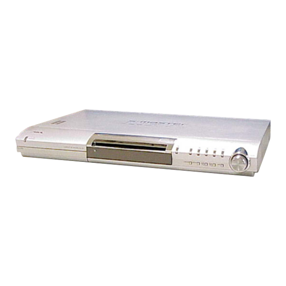
• CX-VX5 are DVD receiver
in AVJ-X5.
Amplifier section
Stereo mode
60 W + 60 W (5 ohms at
1 kHz, THD 10 %)
Surround mode
Front: 60 W + 60 W
Center*: 60 W
Surround*: 60 W + 60 W
(5 ohms at 1 kHz, THD
10 %)
Subwoofer*: 100 W
(3 ohms at 100 Hz, THD
10 %)
* Depending on the sound field settings and the source,
there may be no sound output.
Inputs
VIDEO 1:
Sensitivity: 300 mV
Impedance: 50 kilohms
VIDEO 2:
Sensitivity: 300 mV
Impedance: 50 kilohms
MIC 1/MIC 2:
Sensitivity: 1 mV
Impedance: 10 kilohms
Outputs
VIDEO 1 (AUDIO
OUT):
Voltage: 1 V
Impedance: 1 kilohm
Phones
Accepts low-and high-
impedance headphones.
Sony Corporation
9-877-635-01
2004C04-1
Home Audio Company
© 2004. 03
Published by Sony Engineering Corporation
Model Name Using Similar Mechanism
DVD
DVD Mechanism Type
Section
Optical Pick-up Name
SPECIFICATIONS
DVD system
Laser
Signal format system
Frequency response (at 2 CH STEREO mode)
Harmonic distortion
CX-VX5
AEP Model
UK Model
NEW
CDM80-DVBU24
DBU-1
Semiconductor laser
(DVD: λ=650 nm)
(CD: λ=780 nm)
Emission duration:
continuous
NTSC or NTSC/PAL
DVD (PCM): 2 Hz to 22
kHz (±1.0 dB)
CD: 2 Hz to 20 kHz (±1.0
dB)
Less than 0.03 %
– Continued on next page –
DVD RECEIVER
1
Advertisement
Table of Contents

Related Manuals for Aiwa CX-VX5


Summary of Contents for Aiwa CX-VX5
-
Page 1: Service Manual
CX-VX5 SERVICE MANUAL AEP Model UK Model Ver 1.0 2004. 03 • CX-VX5 are DVD receiver in AVJ-X5. Model Name Using Similar Mechanism DVD Mechanism Type CDM80-DVBU24 Section Optical Pick-up Name DBU-1 SPECIFICATIONS Amplifier section DVD system Stereo mode 60 W + 60 W (5 ohms at... - Page 2 COMPONENTS IDENTIFIED BY MARK 0 OR DOTTED LINE WITH MARK 0 ON THE SCHEMATIC DIAGRAMS AND IN THE PARTS LIST ARE CRITICAL TO SAFE OPERATION. REPLACE THESE COMPONENTS WITH SONY PARTS WHOSE PART NUMBERS APPEAR AS SHOWN IN THIS MANUAL OR IN SUPPLEMENTS PUBLISHED BY SONY.
- Page 3 CX-VX5 CAUTION Use of controls or adjustments or performance of procedures other than those specified herein may result in hazardous radiation exposure. NOTES ON HANDLING THE OPTICAL PICK-UP BLOCK OR BASE UNIT The laser diode in the optical pick-up block may suffer electrostatic breakdown because of the potential difference generated by the charged electrostatic load, etc.
-
Page 4: Table Of Contents
CX-VX5 TABLE OF CONTENTS 1. SERVICE POSITIONS 6-4. Printed Wiring Board –DVD Mechanism Section (2/2)– ........41 1-1. DVD Mechanism Block ............5 6-5. Schematic Diagram –DVD Mechanism Section (2/2)– ..41 1-2. MICON Board ..............5 6-6. Printed Wiring Board –DMB03 Section (1/2)– ....42 6-7. -
Page 5: Service Positions
CX-VX5 SECTION 1 SERVICE POSITIONS 1-1. DVD MECHANISM BLOCK 1-2. MICON BOARD... -
Page 6: General
CX-VX5 SECTION 2 GENERAL This section is extracted from instruction manual. -
Page 7: Front Panel Display
CX-VX5... - Page 8 CX-VX5...
-
Page 9: Rear Panel
CX-VX5... -
Page 10: Remote
CX-VX5... -
Page 11: Language Code List
CX-VX5... -
Page 12: Dvd Setup Menu List
CX-VX5... -
Page 13: Disassembly
CX-VX5 SECTION 3 DISASSEMBLY Note : Disassemble the unit in the order as shown below. 3-1. TOP COVER (Page 14) 3-2. FRONT PANEL ASSY 3-11. POWER BOARD 3-6. REAR PANEL SECTION (Page 15) (Page 20) (Page 17) 3-10. AMP BOARD 3-3. -
Page 14: Top Cover
CX-VX5 Note : Follow the disassembly procedure in the numerical order given. 3-1. TOP COVER 2 two screws (+BTP 3 x 6) 3 five screws (+BTP 3 x 6) 4 top cover 1 two screws (+BTP 3 x 6) -
Page 15: Front Panel Assy
CX-VX5 3-2. FRONT PANEL ASSY 4 CN104 2 screw (+BVTP 3 x 6) 5 CN106 0 I/O board 9 CN108 1 two screws (+P 3 x 8) 8 CN105 6 CN101 7 CN107 qa CN400 qf CN501 qg lug qh screw... -
Page 16: Fl Board
CX-VX5 3-3. FL BOARD 1 two screws (+P 2.6 x 6) claw 2 sub chassis claw 3 two screws (+P 2.6 x 6) 4 FL board 3-4. P-KEY BOARD, RM BOARD 2 P-KEY board 1 two screws (+P 2.6 x 6) -
Page 17: F-Av Board
CX-VX5 3-5. F-AV BOARD 2 two screws (+P 2.6 x 6) 4 connector bracket 5 F-AV board 3 two screws (+P 2.6 x 6) 1 two screws (+KTP 2.6 x 6) 3-6. REAR PANEL SECTION 7 rear panel section 6 screw... -
Page 18: Micon Board
CX-VX5 3-7. MICON BOARD 7 two screws (+P 3 x 8) 4 CN509 3 CN508 2 CN510 6 two screws (+P 3 x 8) 5 CN506 1 CN505 8 MICON board 9 CN102 3-8. MECHANISM DECK 6 CN701 0 mechanism deck... -
Page 19: Dmb03 Board
CX-VX5 3-9. DMB03 BOARD 5 two screws (+BVTP 3 x 6) 4 two screws (+BVTP 3 x 6) 6 heat sink 3 CN107 2 CN106 1 CN105 7 DMB03 board 3-10. AMP BOARD 3 screw 4 two screws (+BVTP 3 x 6) -
Page 20: Power Board
CX-VX5 3-11. POWER BOARD 1 two screws (+BVTP 3 x 6) 4 three screws (+BVTP 3 x 6) 2 sheet (barrier) 5 POWER board 3 screw (+BVTP 3 x 6) 3-12. CHASSIS (TOP) 4 three screws 1 screw (+BVTP 2.6 × 8) (+BVTP 2.6 ×... -
Page 21: Lever (Loading-R/L)
CX-VX5 3-13. LEVER (LOADING-R/L) spr-T (loading-L) spr-T (loading-R) 5 lever (loading-R) 2 two hooks 4 two hooks 3 lever (loading-L) PRECAUTION DURING LEVER (LOADING-R/L) INSTALLATION Align the horizontal position. lever (loading-L) lever (loading-R) Install the both levers so that they move symmetrically. -
Page 22: Lever (Disc Stop), Disc Sensor Lever
CX-VX5 3-14. LEVER (DISC STOP), DISC SENSOR LEVER 1 gear (cap) 2 gear (IDL-L) PRECAUTION DURING LEVER (DISC STOP) INSTALLATION chassis (top) hole 5 two hooks 3 two claws lever (disc stop) 6 lever (disc stop) hole Install the lever (disc stop) so that the both holes are aligned. -
Page 23: Rf Board
CX-VX5 3-16. RF BOARD 5 RF board 4 wire (flat type) (CN002) 2 wire (flat type) (CN003) 3 wire (flat type) 1 claw (CN001) 3-17. OPTICAL PICK-UP 3 two insulators 1 two step screws (M) 5 optical pick-up (DBU-1) 2 step screw (M) -
Page 24: Base Unit
CX-VX5 3-18. BASE UNIT 4 floating screw (+PTPWHM 2.6) 6 base unit 3 spr-E (holder down) 5 floating screw (+PTPWHM 2.6) 2 lever (CL UP2) 1 screw (+BVTP 2.6 × 8) 3-19. LEVER (BU LOCK) 4 lever (BU lock) 3 three hooks... -
Page 25: Close Lever
CX-VX5 3-20. CLOSE LEVER 1 washer (3-1-0.4) 5 close lever 3 claw 2 spr-E (close lever) 4 shaft (disc stop) 3-21. LEVER (DIR), GEAR (IDL-B) 3 pulley (gear) 2 retaining ring 4 gear (cap) 5 gear (IDL-A) 8 stopper 9 lever (DIR) q;... -
Page 26: Gear (Idl-C)
CX-VX5 3-22. GEAR (IDL-C) 3 gear (IDL-D) 4 three hooks 2 two claws 1 gear (IDL-F) 5 gear (loading lever) 7 gear (IDL-C) 6 claw... -
Page 27: Test Mode
CX-VX5 SECTION 4 TEST MODE [Version Display Mode] [OSD Test Mode] * The software version is displayed. Procedure: Procedure: Press the ?/1 button on the main unit or the ?/1 button on Press three buttons of X , [PRESET +] and [FUNCTION] the remote commander to turn the set on. - Page 28 CX-VX5 [GENERAL DESCRIPTION] 0-1. All (All items continuous check) This menu checks all diagnostic items continuously. Normally, all The Test Mode allows you to make diagnosis and adjustment easily items are checked successively one after another automatically using the remote commander and monitor TV. The instructions, unless an error is found, but at a certain item that requires judgment diagnostic results, etc.
- Page 29 CX-VX5 0-2-4. Model Type 1-1. DVD-SL (single layer) Press the 1 key on the remote commander and insert a DVD single Model name is displayed. (DAV-SCX) layer disc following the message. Then the adjustment will be made 0-2-5. Region through the steps below, then adjusted values will be written to the Model destination code is displayed.
- Page 30 CX-VX5 24. Auto track gain adjust DRIVE MANUAL OPERATION Search Check Note: This mode is used for design, and not used in service fundamen- 25. 32Tj forward tally. 26. 32Tj reverse On the Test Mode Menu screen, press the key on the remote 27.
- Page 31 CX-VX5 2-1. Disc Type 2-1-3. Disc Type CD It sets up so that it may judge as a disc type of specification of the disc with which the set was inserted. Disc Type : CD disc (normal speed, 12 cm)
- Page 32 CX-VX5 2-3. Track/Layer Jump 2-5. EEPROM Write Adjust Track/Layer Jump EEPROM Write Adjust FWD R.Lj L0>L1 REV L.Lj L1>L0 1. Focus Offset 3.500Tj Fine FWD U.Fj L0>L1 2. Focus Gain 4.500Tj Fine REV D.Fj L1>L0 3. Trk. Offset Coarse 5.10kTj Dirc 4.
- Page 33 CX-VX5 2-7. Disc Check Memory EMERGENCY HISTORY On the Test Mode Menu screen, selecting displays the Disc Check Memory information such as servo emergency history. The history information from last 1 up to 10 can be scrolled with 1. SL Disc check the O key or o key.
- Page 34 CX-VX5 MECHA ERROR HISTORY • Error code (bb) 00 : Initializing the mechanism deck. On the Test Mode Menu screen, selecting displays the information 10 : Retry over of eject and loading. of mechanism deck error history. 30 : Open operation in no disc status.
-
Page 35: Electrical Adjustment
CX-VX5 SECTION 5 ELECTRICAL ADJUSTMENT [TEST DISC LIST] Use the following test disc on test mode. TDV-520CSO (DVD-SL): PART No. J-2501-236-A LUV-P01 (CD): PART No. 4-999-032-01 TDV-540C (DVD-DL): PART No. J-2501-235-A Note: Do not use exiting test disc for DVD. -
Page 36: Diagrams
CX-VX5 SECTION 6 DIAGRAMS 6-1. CIRCUIT BOARDS LOCATION F-AV board SCART board I/O board P-KEY board RM board FL board KEY board POWER board AMP board DRIVER board RF board MICON board DMB03 board... - Page 37 CX-VX5 THIS NOTE IS COMMON FOR PRINTED WIRING BOARDS AND SCHEMATIC DIAGRAMS. (In addition to this, the necessary note is printed in each block.) for schematic diagram: for printed wiring boards: • X : parts extracted from the component side.
-
Page 38: Micon Board
CX-VX5 • Waveforms – RF Board – – DM03 Board – 200mV/DIV, 100ns/DIV 1V/DIV, 20ns/DIV 200mV/DIV, 20µs/DIV 3.9Vp-p 800mVp-p 50ns 820mVp-p (DVDRFP) (XTAL) (VDAC 4) IC001 IC901 IC207 <zz.> 500mV/DIV, 1ms/DIV 1V/DIV, 10ns/DIV 200mV/DIV, 20µs/DIV 5.6Vp-p 0.5Vp-p 820mVp-p 37ns (TE) (MO1) <zxx>... -
Page 39: Printed Wiring Board -Dvd Mechanism Section (1/2)
CX-VX5 6-2. PRINTED WIRING BOARD — DVD MECHANISM SECTION (1/2) — • Refer to page 36 for Circuit Boards Location and page 37 for Common Note on Printed Wiring Boards. : Uses unleaded solder. RF BOARD RF BOARD (SIDE A) -
Page 40: Schematic Diagram -Dvd Mechanism Section (1/2)
CX-VX5 6-3. SCHEMATIC DIAGRAM — DVD MECHANISM SECTION (1/2) — • Refer to page 37 for Common Note on Schematic Diagrams and page 38 for Waveforms. R026 C006 C028 C027 C013 C031 CN002 C030 C026 C025 R023 C029 C024 C035... -
Page 41: Printed Wiring Board -Dvd Mechanism Section (2/2)
CX-VX5 6-4. PRINTED WIRING BOARD — DVD MECHANISM SECTION (2/2) — • Refer to page 36 for Circuit Boards Location and page 37 for Common Note on Printed Wiring Boards. : Uses unleaded solder. (Page 58) 6-5. SCHEMATIC DIAGRAM — DVD MECHANISM SECTION (2/2) — • Refer to page 37 for Common Note on Schematic Diagrams. -
Page 42: Printed Wiring Board -Dmb03 Section (1/2)
CX-VX5 6-6. PRINTED WIRING BOARD — DMB03 SECTION (1/2) — • Refer to page 36 for Circuit Boards Location and page 37 for Common Note on Printed Wiring Boards. : Uses unleaded solder. (Page 58) (Page 53) CN101 R218 R217... -
Page 43: Printed Wiring Board -Dmb03 Section (2/2)
CX-VX5 6-7. PRINTED WIRING BOARD — DMB03 SECTION (2/2) — • Refer to page 36 for Circuit Boards Location and page 37 for Common Note on Printed Wiring Boards. : Uses unleaded solder. • Semiconductor Location (Side B) Ref. No. -
Page 44: Schematic Diagram -Dmb03 Section (1/8)
CX-VX5 6-8. SCHEMATIC DIAGRAM — DMB03 SECTION (1/8) — • Refer to page 37 for Common Note on Schematic Diagrams. R587 CL505 CL504 CL503 CL502 FL502 CL501 C522 C567 C568 R537 R536 R545 R548 CN501 CL544 R9988 CL537 IC503 R694... -
Page 45: Schematic Diagram -Dmb03 Section (2/8)
CX-VX5 6-9. SCHEMATIC DIAGRAM — DMB03 SECTION (2/8) — • Refer to page 37 for Common Note on Schematic Diagrams. R784 C701 R786 C705 R787 R700 C782 TP703 FL701 R788 FL706 C703 C715 C783 R789 C729 C708 C709 C712 R710... -
Page 46: Schematic Diagram -Dmb03 Section (3/8)
CX-VX5 6-10. SCHEMATIC DIAGRAM — DMB03 SECTION (3/8) — • Refer to page 37 for Common Note on Schematic Diagrams. (Page 44) JL521 R543 R547 R581 C526 C527 (Page 47) R580 R589 C519 (Page 50) R579 IC501 R534 R535 C514... -
Page 47: Schematic Diagram -Dmb03 Section (4/8)
CX-VX5 6-11. SCHEMATIC DIAGRAM — DMB03 SECTION (4/8) — • Refer to page 37 for Common Note on Schematic Diagrams and page 38 for Waveforms. (Page 45) FL901 IC902 (Page 46) R901 C902 C901 Q901 IC904 IC903 R991 CL922 R992... -
Page 48: Schematic Diagram -Dmb03 Section (5/8)
CX-VX5 6-12. SCHEMATIC DIAGRAM — DMB03 SECTION (5/8) — • Refer to page 37 for Common Note on Schematic Diagrams. (Page 45) (Page 50) (Page 47) R270 CN202 (Page 49) IC255 CN105 C283 IC256 (Page 55) R201 R9998 R9999 (Page 46, 49, 50) -
Page 49: Schematic Diagram -Dmb03 Section (6/8)
CX-VX5 6-13. SCHEMATIC DIAGRAM — DMB03 SECTION (6/8) — • Refer to page 37 for Common Note on Schematic Diagrams. (Page 48) JW801 JW601 C344 JW802 JW602 R310 (Page 46) JW803 JW603 C346 C345 R311 JW804 JW604 R312 JW805 JW605... -
Page 50: Schematic Diagram -Dmb03 Section (7/8)
CX-VX5 6-14. SCHEMATIC DIAGRAM — DMB03 SECTION (7/8) — • Refer to page 37 for Common Note on Schematic Diagrams and page 38 for Waveforms. (Page 48) R269 R268 (Page 48) R225 R226 R263 R264 R265 R266 R267 R228 (Page 49) -
Page 51: Schematic Diagram -Dmb03 Section (8/8)
CX-VX5 6-15. SCHEMATIC DIAGRAM — DMB03 SECTION (8/8) — • Refer to page 37 for Common Note on Schematic Diagrams. IC203 C218 RB10 RB12 C220 C255 FL203 C258 C259 C227 FL204 RB13 RB11 C205 C235 IC206 C239 C275 C240 IC216... -
Page 52: Printed Wiring Boards -I/O Section (1/2)
CX-VX5 6-16. PRINTED WIRING BOARDS — I/O SECTION (1/2) — • Refer to page 36 for Circuit Boards Location and page 37 for Common Note on Printed Wiring Boards. : Uses unleaded solder. • Semiconductor Location (Side A) Ref. No. -
Page 53: Printed Wiring Boards -I/O Section (2/2)
CX-VX5 6-17. PRINTED WIRING BOARDS — I/O SECTION (2/2) — • Refer to page 36 for Circuit Boards Location and page 37 for Common Note on Printed Wiring Boards. : Uses unleaded solder. J101 • Semiconductor J104 Location (Side B) Ref. -
Page 54: Schematic Diagram -I/O Section (1/2)
CX-VX5 6-18. SCHEMATIC DIAGRAM — I/O SECTION (1/2) — • Refer to page 37 for Common Note on Schematic Diagrams and page 38 for Waveforms. CN105 R230 R233 TM101 C194 R188 D201 R238 R116 R237 C199 R245 C244 D202 C109... -
Page 55: Schematic Diagram -I/O Section (2/2)
CX-VX5 6-19. SCHEMATIC DIAGRAM — I/O SECTION (2/2) — • Refer to page 37 for Common Note on Schematic Diagrams. (Page 54) L111 IC104 C153 C252 CN106 R169 L115 L122 C169 C187 Q143 C167 IC103 C182 C183 R149 C192 C198... -
Page 56: Printed Wiring Board -F-Av Section
CX-VX5 6-20. PRINTED WIRING BOARD — F-AV SECTION — • Refer to page 36 for Circuit Boards Location and page 37 for Common Note on Printed Wiring Boards. : Uses unleaded solder. • Semiconductor Location Ref. No. Location D809 D810... -
Page 57: Schematic Diagram -F-Av Section
CX-VX5 6-21. SCHEMATIC DIAGRAM — F-AV SECTION — • Refer to page 37 for Common Note on Schematic Diagrams. C838 CN805 R825 L804 R828 R870 Q803 R826 R827 Q805 (Page 61) C840 FB805 R829 J801 FB804 C841 FB806 FB811 Q804... -
Page 58: Printed Wiring Board -Micon Section
CX-VX5 6-22. PRINTED WIRING BOARD — MICON SECTION — • Refer to page 36 for Circuit Boards Location and page 37 for Common Note on Printed Wiring Boards. : Uses unleaded solder. (Page 52) (Page 65) (Page 42) (Page 42) -
Page 59: Schematic Diagram -Micon Section
CX-VX5 6-23. SCHEMATIC DIAGRAM — MICON SECTION — • Refer to page 37 for Common Note on Schematic Diagrams and page 38 for Waveforms. CN511 Q515 Q514 R565 R566 R569 R568 R567 R570 C538 R576 CNP507 R572 R530 (Page R531... -
Page 60: Printed Wiring Boards -Key Section
CX-VX5 6-24. PRINTED WIRING BOARDS — KEY SECTION — • Refer to page 36 for Circuit Boards Location and page 37 for Common Note on Printed Wiring Boards. : Uses unleaded solder. S802 R801 C802 CN804 CN806 D801 CN801 (Page 58) -
Page 61: Schematic Diagram -Key Section
CX-VX5 6-25. SCHEMATIC DIAGRAM — KEY SECTION — • Refer to page 37 for Common Note on Schematic Diagrams. CN804 (Page 57) CN801 D801 CN806 CNP801 C801 C802 R801 FB801 (Page 59) R802 IC801 S802 S801 CN803 C806 R804 C805... -
Page 62: Printed Wiring Board -Fl Section
CX-VX5 6-26. PRINTED WIRING BOARD — FL SECTION — • Refer to page 36 for Circuit Boards Location and page 37 for Common Note on Printed Wiring Boards. : Uses unleaded solder. D802 D803 C816 R820 JR802 D806 R821 C818... -
Page 63: Schematic Diagram -Fl Section
CX-VX5 6-27. SCHEMATIC DIAGRAM — FL SECTION — • Refer to page 37 for Common Note on Schematic Diagrams. FL801 D815 D814 C835 JR806 JR804 T801 R824 R823 JR801 JR802 C821 JR805 C812 D807 R815 R816 R868 C811 D806 R814... -
Page 64: Printed Wiring Board -Amp Section (1/2)
CX-VX5 6-28. PRINTED WIRING BOARD — AMP SECTION (1/2) — • Refer to page 36 for Circuit Boards Location and page 37 for Common Note on Printed Wiring Boards. : Uses unleaded solder. • Semiconductor Location (Side A) Ref. No. -
Page 65: Printed Wiring Board -Amp Section (2/2)
CX-VX5 6-29. PRINTED WIRING BOARD — AMP SECTION (2/2) — • Refer to page 36 for Circuit Boards Location and page 37 for Common Note on Printed Wiring Boards. : Uses unleaded solder. (Page 42) (Page 58) • Semiconductor Location (Side B) Ref. -
Page 66: Schematic Diagram -Amp Section (1/2)
CX-VX5 6-30. SCHEMATIC DIAGRAM — AMP SECTION (1/2) — • Refer to page 37 for Common Note on Schematic Diagrams. CNP305 C460 C461 (Page 70) D396 C396 C467 C439 D397 IC431 IC430 R380 IC432 C430 R430 C434 C431 C437 C436... -
Page 67: Schematic Diagram -Amp Section (2/2)
CX-VX5 6-31. SCHEMATIC DIAGRAM — AMP SECTION (2/2) — • Refer to page 37 for Common Note on Schematic Diagrams. C501 R502 R503 CN502 FAN901 D501 R504 R505 R506 R507 Q502 R508 Q501 C502 R501 D400 D401 C397 IC310 IC311... -
Page 68: Printed Wiring Board -Power Section (1/2)
CX-VX5 6-32. PRINTED WIRING BOARD — POWER SECTION (1/2) — • Refer to page 36 for Circuit Boards Location and page 37 for Common Note on Printed Wiring Boards. : Uses unleaded solder. -
Page 69: Printed Wiring Board -Power Section (2/2)
CX-VX5 6-33. PRINTED WIRING BOARD — POWER SECTION (2/2) — • Refer to page 36 for Circuit Boards Location and page 37 for Common Note on Printed Wiring Boards. : Uses unleaded solder. • Semiconductor Location (Side B) Ref. No. -
Page 70: Schematic Diagram -Power Section
CX-VX5 6-34. SCHEMATIC DIAGRAM — POWER SECTION — • Refer to page 37 for Common Note on Schematic Diagrams. CN902 D911 PT901 L901 D902 C913 R909 C924 IC902 R919 R921 R920 C918 C920 LF901 C907 LF902 R934 TH901 (Page 66) -
Page 71: Exploded Views
CX-VX5 SECTION 7 EXPLODED VIEWS NOTE: • The mechanical parts with no reference • -XX and -X mean standardized parts, so The components identified by mark 0 or dotted line with mark number in the exploded views are not supplied. -
Page 72: Front Panel Section
CX-VX5 7-2. FRONT PANEL SECTION not suplied not suplied not suplied not suplied Ref. No. Part No. Description Remark Ref. No. Part No. Description Remark 4-248-076-01 PANEL, FRONT A-4741-725-A SWITCH ASSY, POWER 4-248-081-01 HOLDER, KNOB A-4749-691-A P-KEY BOARD, COMPLETE 4-248-080-01 KNOB, VOLUME... -
Page 73: Rear Panel Section
CX-VX5 7-3. REAR PANEL SECTION not supplied FC901 FAN901 FC903 not supplied TM101 The components identified by mark 0 or dotted line with mark 0 are critical for safety. Replace only with part number specified. Ref. No. Part No. Description Remark Ref. -
Page 74: Chassis Section-1
CX-VX5 7-4. CHASSIS SECTION-1 CDM80-DVBU24 not supplied not supplied FC902 not supplied Ref. No. Part No. Description Remark Ref. No. Part No. Description Remark A-4749-704-A DMB03 BOARD, COMPLETE FC902 1-500-657-11 CORE, FERRITE A-4749-701-A MICON BOARD, COMPLETE 7-685-645-79 SCREW +BVTP 3X6 TYPE2 N-S... -
Page 75: Chassis Section-2
CX-VX5 7-5. CHASSIS SECTION-2 not supplied FC904 not supplied Ref. No. Part No. Description Remark Ref. No. Part No. Description Remark 4-248-134-01 FOOT 1-775-140-11 WIRE (FLAT TYPE) (15 CORE) A-4749-703-A POWER BOARD, COMPLETE FC904 1-500-826-11 CORE, FERRITE A-4749-699-A AMP BOARD, COMPLETE... -
Page 76: Dvd Mechanism Deck Section-1
CX-VX5 7-6. DVD MECHANISM DECK SECTION-1 (CDM80-DVBU24) CD mechanism section-2 (CDM80-DVBU24) M701 CD mechanism section-3 (CDM80-DVBU24) base unit section Ref. No. Part No. Description Remark Ref. No. Part No. Description Remark 4-985-672-01 SCREW (+PTPWHM2.6), FLOATING 4-245-630-01 LEVER (SW) 4-248-723-01 SPR-E (HOLDER DOWN) 4-951-620-01 SCREW (2.6X8), +BVTP... -
Page 77: Dvd Mechanism Deck Section-2
CX-VX5 7-7. DVD MECHANISM DECK SECTION-2 (CDM80-DVBU24) not supplied Ref. No. Part No. Description Remark Ref. No. Part No. Description Remark 4-245-627-01 WASHER (6-2.7-0.4) 4-245-640-01 GEAR (CAP) 4-245-637-01 ROLLER, RUBBER 4-245-626-01 CAP, CLAMPER (DBU-1) 4-245-649-01 GEAR (IDL-I) 4-245-638-01 LEVER (CL UP1) 4-245-657-01 LEVER (LOADING-R) 4-985-672-01 SCREW (+PTPWHM2.6), FLOATING... -
Page 78: Dvd Mechanism Deck Section-3
CX-VX5 7-8. DVD MECHANISM DECK SECTION-3 (CDM80-DVBU24) supplied supplied Ref. No. Part No. Description Remark Ref. No. Part No. Description Remark 4-245-643-01 GEAR (IDL-C) 4-245-640-01 GEAR (CAP) X-4955-497-2 CHASSIS (BOTTOM) ASSY 4-245-628-01 LEVER (BU LOCK) 4-248-722-01 SPR-E (DIR) 4-248-206-01 WASHER (3-1-0.4) -
Page 79: Base Unit Section
CX-VX5 7-9. BASE UNIT SECTION The components identified by mark 0 or dotted line with mark 0 are critical for safety. Replace only with part number specified. Ref. No. Part No. Description Remark Ref. No. Part No. Description Remark A-4728-690-A RF BOARD, COMPLETE... -
Page 80: Electrical Parts List
CX-VX5 SECTION 8 ELECTRICAL PARTS LIST NOTE: • Due to standardization, replacements in • Items marked “*” are not stocked since The components identified by mark 0 or dotted line with mark the parts list may be different from the they are seldom required for routine service. - Page 81 CX-VX5 Ref. No. Part No. Description Remark Ref. No. Part No. Description Remark C394 1-131-704-11 FILM C475 1-109-982-11 CERAMIC CHIP C395 1-131-704-11 FILM C477 1-109-982-11 CERAMIC CHIP C396 1-162-970-11 CERAMIC CHIP 0.01uF C478 1-109-982-11 CERAMIC CHIP C397 1-216-864-11 METAL CHIP...
- Page 82 CX-VX5 Ref. No. Part No. Description Remark Ref. No. Part No. Description Remark D342 6-500-060-01 DIODE P6SMB36AT3 L303 1-456-667-11 COIL, CHOKE 10uH D343 6-500-060-01 DIODE P6SMB36AT3 L304 1-456-667-11 COIL, CHOKE 10uH D344 6-500-060-01 DIODE P6SMB36AT3 L305 1-456-667-11 COIL, CHOKE 10uH...
- Page 83 CX-VX5 DMB03 Ref. No. Part No. Description Remark Ref. No. Part No. Description Remark R408 1-216-837-11 METAL CHIP 1/10W C151 1-126-206-11 ELECT CHIP 100uF 6.3V R409 1-216-837-11 METAL CHIP 1/10W C204 1-164-947-11 CERAMIC CHIP 0.01uF R410 1-216-826-11 METAL CHIP 2.7K...
- Page 84 CX-VX5 DMB03 Ref. No. Part No. Description Remark Ref. No. Part No. Description Remark C283 1-164-947-11 CERAMIC CHIP 0.01uF C547 1-107-725-11 CERAMIC CHIP 0.1uF C284 1-164-947-11 CERAMIC CHIP 0.01uF C548 1-164-943-11 CERAMIC CHIP 0.01uF C286 1-164-947-11 CERAMIC CHIP 0.01uF C551 1-125-891-11 CERAMIC CHIP 0.47uF...
- Page 85 CX-VX5 DMB03 Ref. No. Part No. Description Remark Ref. No. Part No. Description Remark C764 1-107-820-11 CERAMIC CHIP 0.1uF D394 8-719-988-61 DIODE 1SS355TE-17 C765 1-125-777-11 CERAMIC CHIP 0.1uF D901 8-719-988-61 DIODE 1SS355TE-17 C766 1-164-874-11 CERAMIC CHIP 100PF D1201 8-719-988-61 DIODE 1SS355TE-17...
- Page 86 CX-VX5 DMB03 Ref. No. Part No. Description Remark Ref. No. Part No. Description Remark IC904 6-702-563-01 IC TC7W74FK-TE85L R222 1-216-864-11 METAL CHIP 1/10W IC906 6-700-407-01 IC SM8707GV-G-E2 R223 1-216-864-11 METAL CHIP 1/10W IC907 8-759-583-47 IC uPC2933T-E2 R224 1-216-864-11 METAL CHIP...
- Page 87 CX-VX5 DMB03 Ref. No. Part No. Description Remark Ref. No. Part No. Description Remark R310 1-216-809-11 METAL CHIP 1/10W R554 1-216-864-11 METAL CHIP 1/10W R311 1-216-809-11 METAL CHIP 1/10W R555 1-216-864-11 METAL CHIP 1/10W R312 1-216-809-11 METAL CHIP 1/10W R558...
- Page 88 CX-VX5 DMB03 Ref. No. Part No. Description Remark Ref. No. Part No. Description Remark R725 1-216-824-11 METAL CHIP 1.8K 1/10W R908 1-216-833-11 METAL CHIP 1/10W R726 1-216-845-11 METAL CHIP 100K 1/10W R910 1-216-864-11 METAL CHIP 1/10W R727 1-216-827-11 METAL CHIP 3.3K...
- Page 89 CX-VX5 DMB03 DRIVER F-AV Ref. No. Part No. Description Remark Ref. No. Part No. Description Remark R9980 1-216-864-11 METAL CHIP 1/10W A-4749-695-A F-AV BOARD, COMPLETE R9981 1-216-864-11 METAL CHIP 1/10W ******************** R9982 1-216-864-11 METAL CHIP 1/10W R9983 1-216-864-11 METAL CHIP 1/10W <...
- Page 90 CX-VX5 F-AV Ref. No. Part No. Description Remark Ref. No. Part No. Description Remark < IC > R866 1-216-864-11 METAL CHIP 1/10W R867 1-216-841-11 METAL CHIP 1/10W IC803 8-759-100-96 IC uPC4558G2 R869 1-216-841-11 METAL CHIP 1/10W IC804 8-759-539-45 IC M62429P...
- Page 91 CX-VX5 Ref. No. Part No. Description Remark Ref. No. Part No. Description Remark < FLUORESCENT INDICATOR > C140 1-126-926-11 ELECT 1000uF C142 1-126-926-11 ELECT 1000uF FL801 1-518-913-11 INDICATOR TUBE, FLUORESCENT C144 1-126-926-11 ELECT 1000uF C148 1-126-926-11 ELECT 1000uF < IC >...
- Page 92 CX-VX5 Ref. No. Part No. Description Remark Ref. No. Part No. Description Remark C219 1-162-915-11 CERAMIC CHIP 10PF 0.5PF < COIL > C220 1-164-156-11 CERAMIC CHIP 0.1uF C226 1-162-970-11 CERAMIC CHIP 0.01uF L101 1-456-700-11 COIL, BALUN C227 1-162-915-11 CERAMIC CHIP 10PF 0.5PF...
- Page 93 CX-VX5 Ref. No. Part No. Description Remark Ref. No. Part No. Description Remark R127 1-216-839-11 METAL CHIP 1/10W R227 1-216-839-11 METAL CHIP 1/10W R128 1-216-821-11 METAL CHIP 1/10W R229 1-216-821-11 METAL CHIP 1/10W R129 1-216-821-11 METAL CHIP 1/10W R230 1-216-809-11 METAL CHIP...
- Page 94 CX-VX5 MICON Ref. No. Part No. Description Remark Ref. No. Part No. Description Remark < RESISTOR > C539 1-164-156-11 CERAMIC CHIP 0.1uF C540 1-164-156-11 CERAMIC CHIP 0.1uF R804 1-216-864-11 METAL CHIP 1/10W C541 1-126-933-11 ELECT 100uF R805 1-216-821-11 METAL CHIP...
- Page 95 CX-VX5 MICON Ref. No. Part No. Description Remark Ref. No. Part No. Description Remark < FERRITE BEAD > R538 1-216-833-11 METAL CHIP 1/10W R539 1-216-841-11 METAL CHIP 1/10W FB502 1-414-813-11 FERRITE, EMI (SMD) R540 1-216-833-11 METAL CHIP 1/10W R541 1-216-833-11 METAL CHIP 1/10W <...
- Page 96 CX-VX5 MICON P-KEY POWER Ref. No. Part No. Description Remark Ref. No. Part No. Description Remark R605 1-216-809-11 METAL CHIP 1/10W A-4749-703-A POWER BOARD, COMPLETE R606 1-216-864-11 METAL CHIP 1/10W *********************** R607 1-216-864-11 METAL CHIP 1/10W R608 1-216-864-11 METAL CHIP...
- Page 97 CX-VX5 POWER Ref. No. Part No. Description Remark Ref. No. Part No. Description Remark < DIODE > L908 1-414-398-11 INDUCTOR 10uH L909 1-456-182-11 COIL, CHOKE 100uH D801 8-719-820-05 DIODE 1SS181 L911 1-414-398-11 INDUCTOR 10uH D802 8-719-801-78 DIODE 1SS184 L912 1-414-398-11 INDUCTOR...
- Page 98 CX-VX5 POWER Ref. No. Part No. Description Remark Ref. No. Part No. Description Remark R924 1-216-818-11 METAL CHIP 1/10W C027 1-107-826-11 CERAMIC CHIP 0.1uF R925 1-216-813-11 METAL CHIP 1/10W C028 1-107-826-11 CERAMIC CHIP 0.1uF R926 1-216-845-11 METAL CHIP 100K 1/10W...
- Page 99 CX-VX5 SCART Ref. No. Part No. Description Remark Ref. No. Part No. Description Remark R020 1-216-864-11 METAL CHIP 1/10W MISCELLANEOUS R021 1-216-864-11 METAL CHIP 1/10W *************** R022 1-216-813-11 METAL CHIP 1/10W R023 1-216-820-11 METAL CHIP 1/10W 1-765-325-11 WIRE (FLAT TYPE) (11 CORE)
- Page 100 CX-VX5 REVISION HISTORY Clicking the version allows you to jump to the revised page. Also, clicking the version at the upper on the revised page allows you to jump to the next revised page. Ver. Date Description of Revision 2004. 03...
Need help?
Do you have a question about the CX-VX5 and is the answer not in the manual?
Questions and answers