Table of Contents
Advertisement
Quick Links
MITSUBISHI ELECTRIC
CAUTION:
Before servicing this chassis, it is important that the service person read the "SAFETY PRECAUTIONS" and
"PRODUCT SAFETY NOTICE" contained in this manual.
• Power
: AC 120V, 50/60Hz
480W (Typical)
5.4A (Maximum)
• Signals
Sync Range
: Horiz : 15.5 to 93.8 kHZ
(Automatic : step scan)
: Vert : 50.0 to 120 Hz
(Automatic : step scan)
Input Signals
: RGB, HD*
DVD*
• Input Terminals
RGB
: Visual 1 (Analog) : Mini D-sub 15-pin
Visual 2 (Analog) : BNC (R,G,B,H/CS,V)*
Visual 3 (M-LINK) : MONITORLINK
Video
: Visual 1 : RCA-pin
Visual 2 : BNC
Visual 3 : S-Video: DIN 4-pin
DVD/HD/DTV
: Visual 1 RCA-pin (Y,PB[CB},PR{CR])*
Visual 2 BNC (Y,PB[CB},PR{CR])*
Audio
: Stereo RCA x 3 (Selectable)
External Control
: D-sub 9-pin (RS232C)
• Weight and dimensions shown are approximate.
• Design specifications are subject to change without notice.
MITSUBISHI DIGITAL ELECTRONICS AMERICA, INC.
Copyright © 2002 Mitsubishi Digital Electronics America, Inc.
SPECIFICATIONS
1
,
1
, DTV*
1
1
9351 Jeronimo Road, Irvine, CA 92618-1904
All Rights Reserved
Service
Manual
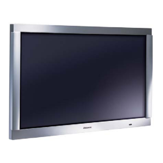
PLASMA DISPLAY PANEL
PD-5010
• Sound Output : 7W+7W at 6 ohms
• Dimensions
• Weight
*1
HD/DVD/DTV Input Signa ls supporte d:
480P (60Hz)
525P (60Hz)
2
576P (50Hz)
TM
625P (50Hz)
720P (60Hz)
1080I (50Hz)
1
*
*2
The 5-BNC conne ctors a re use d a s
RGB/PC2 a nd HD/DVD2 input.
Se le ct one of the m unde r "BNC SELECT".
: (W)49.5" (H)30.2" (D)4.68"
(W)1257 (H)766 (D)119 mm
: 98 lbs / 44.5 kg
480I (60Hz)
525I (60Hz)
576I (50Hz)
625I (50Hz)
1035I (60Hz)
1080I (60Hz)
2002
2002
2002
2002
2002
Advertisement
Table of Contents

Related Manuals for Mitsubishi Electric PD-5010


Summary of Contents for Mitsubishi Electric PD-5010
-
Page 1: Service Manual
2002 2002 2002 2002 2002 Service MITSUBISHI ELECTRIC Manual PLASMA DISPLAY PANEL PD-5010 CAUTION: Before servicing this chassis, it is important that the service person read the "SAFETY PRECAUTIONS" and "PRODUCT SAFETY NOTICE" contained in this manual. SPECIFICATIONS • Power : AC 120V, 50/60Hz •... -
Page 3: Table Of Contents
CONTENTS SAFETY PRECAUTIONS ..........................2-1 TROUBLESHOOTING............................3-1 METHOD OF ADJUSTMENTS........................... 4-1 METHOD OF DISASSEMBLY..........................5-1 PACKAGING............................... 6-1 PART LIST................................7-1 CONNECTION DIAGRAMS..........................8-1 BLOCK DIAGRAM.............................. 9-1... -
Page 4: Safety Precautions
SAFETY PRECAUTIONS CAUTION RISK OF ELECTRIC SHOCK DO NOT OPEN CAUTION: TO REDUCE THE RISK OF ELECTRIC SHOCK, DO NOT OPEN REAR COVER. NO USER-SERVICEABLE PARTS INSIDE. REFER SERVICING TO QUALIFIED SERVICE PERSONNEL. This symbol warns the user that unin- This symbol alerts the user that important sulated voltage within the unit may have literature concerning the operation and... - Page 5 SAFETY PRECAUTIONS 1. Before returning an instrument to the customer, al- AC Leakage Test ways make a safety check of the entire instrument, in- cluding, but not limited to, the following items. (READING SHOULD NOT BE ABOVE 3.5 mA) a. Be sure that no built-in protective devices are LEAKAGE DEVICE CURRENT...
- Page 6 SAFETY PRECAUTIONS 5. Observe original lead dress. Take extra care to assure correct lead dress in the following areas: a. near sharp edges, b. near thermally hot parts— be sure that leads and components do not touch thermally hot parts, c. the AC supply, d. high volt- age, and e.
- Page 7 PRECAUTIONS DE SECURITE 1. Avant de remettre un appareil à un client, faire courant ne doit dépasser 3.5 milliamp. Inverser la toujours d'abord un examen de sécurité de fiche de courant de l'appareil dans la prise et l'appareil en entier comprenant, mais ne s'y limitant répéter le test.
- Page 8 PRECAUTIONS DE SECURITE b. Certains châssis de moniteur ont habituellement 6. Les composants, parts (pièces) et/ou fils qui ont été 85V (RMS) entre le châssis et la prise de terre, en trouvés surchauffés devraient être remplacés avec fonction de la polarité de la prise de courant. Ces les composants, pièces et fils s'y reliant avec d'autre châssis peuvent ne comporter aucun risque qui ont les mêmes spécifications que les originales.
- Page 10 SAFETY PRECAUTIONS (Notes) The component by the name of “module” used in this product is defined as a section that is pro- vided with a digital circuit board (including high- voltage parts) used to emit light in the glass panel part, excluding the surface acrylic fiIter or the tem- pered glass fiIter.
-
Page 11: Troubleshooting
TROUBLESHOOTING... - Page 12 TROUBLESHOOTING • In the case of abnormality in the POWER system, such as “No power available” or “Alarm (LED flashing)” Go to 1. Power failure (P2) • In the case of abnormality in the VIDEO system, such as “No picture” or “Picture errors” Go to 2.
-
Page 13: Power Failure
1. Power failure (1) POWER is turned OFF. Note: To Reset the Microprocessor, Press and hold the <Power On> and <Input> keys on the front panel at the same time. Hold for 5 to 6 seconds. Turn on the main power unit. Is the POWER LED lit? Is the power plug connected Poor power plug connection... - Page 14 (Caution) When the LED is flashing (protector in operation), all power lines other than M+7 are automatically turned off. When checking the power lines other than the M+7V system, a circuit tester or the like should be connected to the measuring point in advance, for confirmation. (2) Flashing in green (FAN error detection) Does the fan run when the main Is the power supply available...
- Page 15 (3) Flashing in red (Temperature error detection) In the cold-start mode, does it Is Potential 0V maintained IC7001 and peripheral take less than 15 seconds after at Pin 29 (MAIN) of IC7001? circuits are out of order. the main power circuit is turned ON and until it is turned OFF? TH1 in the POWER unit and Disconnect the PD, PH, and...
- Page 16 (4) Flashing in green and red (Panel crack detection) Is Potential 0V maintained at IC7001 and peripheral Pin 100 (MAIN) of IC7001? circuits are out of order. Is Potential 0V maintained at Is Potential 5V applied to IC7002 and peripheral (MAIN) of IC7002? of IC7002? circuits are out of order.
- Page 17 2. No picture displayed and picture errors (Caution) IPXXXX is installed in the MAIN PWB and the VIDEO PWB. These components are inserted in the power line. If there is any error occurring in the circuit, these components function to prevent the evolution of this problem to other areas.
- Page 18 (1)-1 (P6) Are the signals below available at Pins 2, 5, 8, 3, Are the specified voltages available at the 6, and 9 of the BU connector? PV connector? Pin 1 14Vdc Pin 3 5Vdc Pin 5 6Vdc 2, 5, 8 Pin 7 7Vdc 5Vp-p...
- Page 19 (2) No picture display of the VIDEO signal only Enter an input of gray scale in the input circuit of VIDEO1, and select VIDEO1. Is a signal of about 3Vp-p available at any of The MAIN PWB is out of order. Pins 21 to 79 of the AM connector in the DSP PWB (GND terminal excluded)? •...
- Page 20 (2)-1 (P8) Are the signals below available at Pins 14 to 17, The DSP PWB is out of order. 19, 98, 96, 95, and Pin 3 (IP8001) of the AM connector in the DSP PWB? 5Vp-p 5Vp-p 3Vp-p 5Vdc 10MHz, 3Vp-p 27MHz, 3Vp-p 15KHz, 3Vp-p 60Hz, 3Vp-p...
- Page 21 (2)-2 (P9) Are the signals below available at Pins 2, 5, 8, 3, Are the specified voltages available at the 6, and 9 of the BU connector? PV connector? Pin 1 14Vdc Pin 3 5Vdc Pin 5 6Vdc 2, 5, 8 Pin 7 7Vdc 5Vp-p...
- Page 22 No presentation of pictures and ON-screen display (P6) Are pulses of 3Vp-p available at Pins 38, 39, and 40 of the AD connector? Are the horizontal/vertical sync signals of 3Vp-p available at Pins 27/28 of IC8701, and a clock signal at Pin 31? 50KHz 60Hz 40MHz...
- Page 23 (3) Picture errors Display a picture in error mode. However, the video signal level shall be maintained above 0.7Vp-p. 0.7Vp-p or above Are pulses of 3Vp-p available at Pins 38, 39, and 40 of the AD connector? Are the horizontal/vertical sync signals of 3Vp-p available at Pins 27/28 of IC8701, and a clock signal at Pin 31? 50KHz...
- Page 24 (3)-1 (P12) Does this phenomenon correspond to “Specific gradations (brightness) are tinted.”? Are the signals of 3Vp-p (signal name:REV_ (3)-2 (P14) LVDS, RODD_LVDS, etc.) available at all the signal input pin of IC8701 and IC8702? • • • • • • Is a signal of about 3Vp-p available at all Pins 21 The MAIN PWB is out of order.
- Page 25 (3)-2 (P13) Is normal display available when the AD, PD, or Each cable is defective. PH cable is replaced? Is normal display available when the MAIN PWB The MAIN PWB is out of order. is replaced? Are 170V, 64V, and D+5V of the POWER unit See “Power cannot be ON.”...
- Page 26 3. No audio output generated Note) This model is enabled to set up an audio input terminal for each video input terminal. No audio output is available unless the input terminal of the displayed pictures (example: VIDEO 1) coincides with that of audio (example: RGB 3).
-
Page 27: Method Of Adjustments
METHOD OF ADJUSTMENTS... - Page 28 Adjusting conditions Adjustments should be carried out in accordance with the procedures described below. However, any adjustments other than the items A to C below are not required. A. When the [PDP module] is replaced, adjust the sections according to the adjusting items [1 to 3] specified below. (Caution) When the PDP module has been replaced, clear the USAGE TIME to “0”...
- Page 29 2. Adjustment of +64V (1) Using any video signal of VIDEO input, DVD/HD input, or RGB input, and display a color bar signal. Turn on the power switch of the main unit. (2) Confirm that the voltage at TP4 (D+60V output) and TP2 (D.GND) of the power unit is maintained at a voltage value (Vd value of the label described in Item 1 above) within ±...
-
Page 30: Initial Setting
[<] and [>]. J : JAPAN JW : OEM Specifications for Japan A : NORTH AMERICA AW : MITSUBISHI PD-5010 G : EUROPE GW : OEM Specifications for Europe FUNCTION... - Page 31 [Initial setting values] (User setting values) Mode J, JW Other than J, JW Remote control standby ON condition ON condition Sound volume 10 steps 10 steps Input mode VIDEO1 VIDEO1 Display mode STRETCHED STRETCHED AUTO picture OFF (All of RGB1 to 3) OFF (All of RGB1 to 3) HD select 1080B...
- Page 32 5. Adjustment of VIDEO screen position and phase 5-1. Adjustment of VIDEO screen position (Caution) Adjustments should be started after returning the [VIDEO] and [SCREEN] setting of the main menu to the initial setting conditions. (1) Enter an input of NTSC and PAL monoscopic signals in VIDEO 1 and use the [FORMAT] key of the remote control to change over the screen size in the sequential order of [STRETCHED ZOOM NARROW...
- Page 33 (11) In the same manner, press the FORMAT key and select [NARROW STANDARD STRETCHED ZOOM SCAN] in this order. Adjust the screen position so that the screen can be arranged evenly to the top, bottom, right, and left. Confirm that [H PHA] and [H CLK] are 0. Otherwise, press the cursor keys [<] and [>] to adjust them to 0.
- Page 34 (6) Select the DTV 720P signal for the input video signal. Confirm that the screen position is uniformly arranged to the top, bottom, right, and left. If the screen position is found to be unevenly arranged, make adjustments according to the “method of screen position adjustment”...
- Page 35 The PWB-SCAN and PWB-COMMON are included together. Replace both PWB's at the same time. After replacment, perform the Vsw, Vp+, and Vbw adjustments in the order described. Voltage Label Check 1. Prior to adjustment, note the voltage levels recorded on the Voltage Label as shown. Vbw Vsw Vp+ Example: Vbw :...
- Page 36 Vp+ & Vbw Adjustments... PWB-SCAN Note: Measure voltage between the TP and closest Chassis Ground. 1. Vp+ - Adjust VR1 so the voltage at TP33 is set to the level specified for Vp+ on the Voltage Label +/- 0.5V. 2. Vbw - Adjust VR2 so the voltage at TP34 is set to the level specified for Vbw on the Voltage Label +/- 0.5V. TP33 PWB-SCAN TP34...
-
Page 37: Video Input
[Morgue] 1. Signal Generator (1) Digital RGB and component signal generator ¥ Equivalent to the Video Generator LT1615 (made by LEADER) ¥ Equivalent to the Panel Adapter LT9217 (made by LEADER) ¥ Equivalent to the Video Encoder LT1606 (made by LEADER) (2) NTSC signal generator ¥... - Page 38 4. RGB/PC input Horizontal sync period Video signal 0.7Vp-p Sync signal TTL level Positive/negative polarity (2) Vertical sync period Video signal 0.7Vp-p Sync signal TTL level Positive/negative polarity * The data a to j above are specified in the next page and thereafter, classified for various inspection signals.
- Page 39 5. RGB/PC signal timing table PC mode Signal name VU-6010 VU-6010 PC98 PC98 NTSC PAL/SECAM 400@56Hz 400@70Hz 480@60HZ Definition 640*240 768*288 640*400 640*400 640*480 Dot clock frequency (MHz) 12.214 14.752 21.053 25.175 25.175 H frequency (kHz) 15.734 15.557 24.826 31.469 31.469 V frequency (Hz) 59.94...
- Page 40 PC mode Signal name MAC@13Ó VESA VESA VESA XGA-2 480@72Hz 480@75Hz 480@85Hz 480@75HZ Definition 640*480 640*480 640*480 640*480 640*480 Dot clock frequency (MHz) 30.24 31.5 31.5 36.0 31.5 H frequency (kHz) 37.861 37.5 43.269 39.375 V frequency (Hz) 66.667 72.809 85.008 H total (uS) 28.571...
- Page 41 PC mode Signal name VESA VESA VESA VESA VESA 600@56Hz 600@60Hz 600@72Hz 600@75Hz 600@85Hz Definition 800*600 800*600 800*600 800*600 800*600 Dot clock frequency (MHz) 49.5 56.25 H frequency (kHz) 35.156 37.879 48.077 46.875 53.674 V frequency (Hz) 56.25 60.317 72.188 85.061 H total (uS) 28.444...
- Page 42 PC mode Signal name MAC@16Ó I/O dater CEREB VESA wide VESA wide wide wide 1 (NEC 1) (NEC 2) Definition 832*624 852*480 864*480 848*480 1024*576 Dot clock frequency (MHz) 57.2832 34.006 42.526 33.75 47.25 H frequency (kHz) 49.725 31.722 37.5 31.02 35.795 V frequency (Hz)
- Page 43 PC mode Signal name VESA wide VESA wide CEREB VESA VESA (NEC 3) (NEC 4) wide 2 768@60Hz 768@70Hz Definition 1280*720 1360*768 1024*600 1024*768 1024*768 Dot clock frequency (MHz) 76.5 85.5 51.2 H frequency (kHz) 45.106 47.712 37.879 48.363 56.476 V frequency (Hz) 60.142 60.015...
- Page 44 PC mode Signal name VESA VESA MAC@19Ó VESA VESA 768@75Hz 768@85Hz 1024@60Hz 1024@75Hz Definition 1024*768 1024*768 1024*768 1280*1024 1280*1024 Dot clock frequency (MHz) 78.75 94.5 H frequency (kHz) 60.023 68.677 60.24 63.981 79.976 V frequency (Hz) 75.029 84.997 74.93 60.02 75.025 H total (uS) 16.66...
- Page 45 PC mode Signal name IDC-3000G IDC-3000G HDTV-J DTV (480P) DTV (720P) PAL 625P NTSC 525P Definition 768*576 640*480 1920*1034 644*483 1280*720 Dot clock frequency (MHz) 29.687 24.39 74.25 24.37 74.25 H frequency (kHz) 31.389 31.47 33.75 31.469 45.000 V frequency (Hz) 59.9 60/60 59.94...
- Page 46 PC mode Signal name HDTV-W SSPE JSPE MAC@12Ó Definition 1920*1080 1024*512 852*480 1152*870 Dot clock frequency (MHz) 74.25 H frequency (kHz) 33.75 33.727 15.75 68.681 V frequency (Hz) 60/60 60.012 59.94 75.062 H total (uS) 29.630 29.650 63.750 14.560 (dots) 2200 1186 1020...
-
Page 47: Method Of Disassembly
METHOD OF DISASSEMBLY (Cautions) 1. Before disassembly, turn power off the main unit and pull out the power plug from the wall outlet. 2. Use a screwdriver with a fitting size. Otherwise, the screw threads may be damaged. 3. Reassembly can be carried out in the reverse order for disassembly. Refer to the disassembly procedures and forward reassembly in the reverse order. - Page 48 1.LABEL SUPPLEMENT SHEET (M62) FILAMENT TAPE(9mm*50m) NAME PLATE(M53) SPEAKER LABEL(M54) LABEL (EARTH) (M65) SERIAL LABEL(M10) LABEL A (2001) (M66) LABEL (OUT) (M64) AC IN LABEL(M55) 2.BACK COVER (1)PL-CPIMS*4*12*15KF(SRW36) FELTSHHET(M69) STAND REAR SIDE TERMINAL LABEL B (M57) (3) BACK COVER (M58) (2)PL-CPIMS*3*6*3KF(SRW35) GASKET L=200 GASKET L=250...
- Page 49 EDGE SADDLE(M06) (5)TP-M4*8*3KF(SRW13) (Caution) At the time of assembly, it shall be tightened together with the round terminal of the connector CN-AD. (6) TERMINAL PANEL (VI) ASSY (M59) Adhesion of the protective tape (Caution) When mounting a back BRACKET (OPTION R) (M44) TP-M4*8*3KF(SRW34) cover, stick the filament tape (30mm*50m) for the...
- Page 50 4. AUDIO AMPLIFIER MODULE SP PWB ASSY (PWC-4419E) (A12) LED PWB ASSY (PCB-4419B) (A11) TERMINAL PANEL (SP) (M61) TP-M3*6*3KF(SRW24) CBIPS*4*12*3KF (SRW02) TP-M4*8*3KF(SRW37) CBIPS*3*8*3KF(SRW23) CTL PWB ASSY (PCB-4419B) (A09) (1)TP-M3*6*3KF(SRW21) GASKET (L70*10*T1) (M17 (GSK09)) MESH (M47) (3)AUDIO AMPLIFIER MODULE(A_UNIT) (2)SCREW,P-CPIMS*3*14*3KF(SRW22) • AC INLET ASSY ET-CBIMS*4*8*3KF(SRW26) CABLE 1P(E02) 07S530015 Green CABLE...
- Page 51 5. POWER UNIT TP-M4*8*3KF(SRW39,40) *2 x 2 SENS PWB ASSY(PCB-5023C)(A04) PLATE(M48) SENT PWB ASSY(PCB-5023D)(A05) SENS PWB ASSY PLATE SENT PWB ASSY (2)BRACKET(POWER)(M41) INSULATORD4.5*T1)(M67) (3) TP-M4*8*3KF (SRW09) (4)POWER UNIT(A13) (1)TP-M4*8*3KF(SRW10) 6.PDP MODULE (11)FRAME(T)(M34) (10)TP-M4*8*3KF(SRW07) (4)TP-M4*8*3KF(SRW04) CN 10P(PD) (CN-PD) CN 9P(PH)(CN-PH) STOP UP SHEET(M71) (6)TP-M4*8*3KF(SRW05) (1)PL-CPIMS*4*16*3GF(SRW03) *4 x 2...
- Page 52 (8) TP-M3*6*3KF(SRW38) CLAMPER, WIRE (M04) (Caution) Make a connection where no "AD" label is present. (14) PDP-NP50C2MF01 (P01) TAPE 1150mm*2 (30m) 7.FRONT PANEL ASSY/FILTER (2) BRACKET FILTER (T) (M38) (1)CBIPS*4*12*3KF(SRW01) (3)BRACKET FILTER(S)(M40) TAPE 680mm x 2 (30m) (2) CUSHION (10*5*600) (M49) (4) BRACKET FILTER (B) (M39) A=10 ±...
- Page 53 WIRING DIAGEAM Wind the TR by one turn Fix the PD, PH Fixed to the vicinity of the sensor PWB Fix the AD Delete the TR Fix the PH Fix the FAN, PD Fix the PD, PH Fix the surplus Wind the TM by one turn Fixed to the vicinity of the sensor PWB Pass the AD part of the fan...
-
Page 54: Packaging
PACKAGING... - Page 55 1.BAG A BRACKET(SAFE) PL-CPIMS*4*10*3KF 2.BAG B SERVICE STATION GUIDE NOTICE SHEET USER'S MANUAL SUPPLEMENT SHEET 3.BAG C BAG,POLYETHYLENE(150*370) BAG B PLUG BATTERY,DRY CELL UM-4*2 CORE,FERRITE FERRITE CORE...
- Page 56 4. ACCESSORY BOX BAG B PLUG CABLE REM-T HAND UNIT POWER CORD CABLE,D-SUB 15P L1800 BAG C ACCESSORY BOX...
- Page 57 5.CARTON BOX FRONT BAR CODE SERIAL LABEL PILLER T SPACER TR SPACER TL PROTECTION SHEET PILLER S SPACER BR SPACER BC ACCESSORY BOX (W) SPACER BL CARTON BOX B PILLER S PILLER T PROTECTION SHEET TAPE...
- Page 58 STOPPER TAPE PP BAND JOINT BAR CODE SERIAL LABEL BACK...
-
Page 59: Parts List
09S900017 PDP-NP50C2MF01 0936P7D01 PWB-DSP ASSY (PCB-5015) 0936P7M01 PWB-MAIN (PCB-5022) 03S110061 PWB-POWER UNIT (A13) 0936P7S91 PWB-SUB ADJ (PWC-4419A) 0936P7V01 PWB-VIDEO (PCB-5023A) 03S120141 REM0TE PDP Break Down PD-5010 Item # Part # Description PDP Location 50C2G1/F1 PWB-(SCAN & COMMON) Center Left & Rt... - Page 60 PD-5010 PDP Assembly Item # Part # Description PDP Location 50C2G1/F1 PWB-(SCAN & COMMON) Center Left & Rt Part Number: 09S900017 50C2E1 PWB-SCAN RELAY (RT) Right Side Top Description: PDP-NP50C2MF01 50C2E2 PWB-SCAN RELAY (RB) Right Side Bottom 50C2J1 PWB-DATA RELAY (TL)
-
Page 61: Connection Diagrams
CONNECTION DIAGRAMS... - Page 62 PD-5010 BLOCK DIAGRAM SENS PWB (PCB-5023C) POWER FAN SEN FAN SET FAN PDP MODULE SENS PWB (PCB-5023D) VIDEO PWB (PCB-5023A) MAIN PWB(PCB-5022) POWER SUPPLY DSP PWB PCB-5015 +25V PWR PWB PANEL PWB (PWC-4419C) (PCB-5023B) 232C PWB (PWC-4419A) SP PWB AUDIO AMP MODULE...
- Page 63 Connector pin descriptions Between PWBs Connector name Pin No. Signal name Acronym Complementary description Signal direction MAIN-VIDEO HDSTP Video mute control of chroma signal Turned LO when the DS connector is available, and video output is generated. Turned HI when no DS connector is available, and video output is muted.
- Page 64 Between PWBs Connector name Pin No. Signal name Acronym Complementary description Signal direction YUMVD Vertical sync signal for microcomputer Vertical sync signal input to be entered in VIDEO MAIN microcomputer when a chroma or video signal is used. YUHD Horizontal sync signal for A/D Horizontal sync signal input to be entered in A/D VIDEO MAIN converter when a chroma or video signal is used.
- Page 65 Between PWBs Connector name Pin No. Signal name Acronym Complementary description Signal direction VIDEO-AUDIO AU_L Signal L L CH for audio signal VIDEO AUDIO AU_R Signal R R CH for audio signal VIDEO AUDIO POMUTE Mute signal for Power start Usually 4.8V VIDEO AUDIO...
- Page 66 Between PWBs Connector name Pin No. Signal name Acronym Complementary description Signal direction VIDEO input F- MAIN PDPMODULE VIDEO input F+ MAIN PDPMODULE VIDEO input G- MAIN PDPMODULE VIDEO input G+ MAIN PDPMODULE RCLK2- CKL2- for VIDEO MAIN PDPMODULE RCLK2+ CKL2+ for VIDEO MAIN PDPMODULE...
- Page 67 Between PWBs Connector name Pin No. Signal name Acronym Complementary description Signal direction D.GND D.GND D.GND D+5V 5V for DIGITAL POWER MAIN D.GND MAIN-LED REMIN1 Infrared ray remote control data MAIN LEDCTL1 Standby LED control MAIN LEDCTL2 Standby LED control MAIN M+5V 5V power supply for microcomputer...
- Page 68 Between PWBs Connector name Pin No. Signal name Acronym Complementary description Signal direction D+170 170V power supply for DIGITAL circuit POWER MODULE No-connection terminal D+70 70V power supply for DIGITAL circuit POWER MODULE 5V power supply for DIGITAL circuit POWER MODULE MIAN-PL (Note : MAIN PWB...
- Page 69 Between PWBs Connector name Pin No. Signal name Acronym Complementary description Signal direction GND2 GND2 GND2 GND2 ENAMDP Not used SCL1 Clock line for the I2C bus For DSP MAIN SDA1 Data line for the I2C bus For DSP MAIN SDA_AMDP Data line for the I2C bus For DSP...
- Page 70 Between PWBs Connector name Pin No. Signal name Acronym Complementary description Signal direction VOUT_GEV2 Digital video signal (G) MAIN VOUT_GEV1 Digital video signal (G) MAIN VOUT_GEV0 Digital video signal (G) MAIN GND2 VIO_RODD7 Digital video signal (R) MAIN VIO_RODD6 Digital video signal (R) MAIN VIO_RODD5 Digital video signal (R)
- Page 71 Between PWBs Connector name Pin No. Signal name Acronym Complementary description Signal direction GND2 VIN_BODD3 Digital video signal (B/Pb) MAIN VIN_BODD2 Digital video signal (B/Pb) MAIN VIN_BODD1 Digital video signal (B/Pb) MAIN VIN_BODD0 Digital video signal (B/Pb) MAIN GND2 VIN_BEV7 Digital video signal (B/Pb) MAIN VIN_BEV6...
- Page 72 Between PWBs Connector name Pin No. Signal name Acronym Complementary description Signal direction VIN_REV7 Digital video signal (R/Pr) MAIN VIN_REV6 Digital video signal (R/Pr) MAIN VIN_REV5 Digital video signal (R/Pr) MAIN VIN_REV4 Digital video signal (R/Pr) MAIN VIN_REV3 Digital video signal (R/Pr) MAIN VIN_REV2 Digital video signal (R/Pr)
-
Page 73: Block Diagram
BLOCK DIAGRAMS... - Page 74 VIDEO PWB...
- Page 75 MAIN PWB...
Need help?
Do you have a question about the PD-5010 and is the answer not in the manual?
Questions and answers