Sign In
Upload
Download
Table of Contents
Contents
Add to my manuals
Delete from my manuals
Share
URL of this page:
HTML Link:
Bookmark this page
Add
Manual will be automatically added to "My Manuals"
Print this page
×
Bookmark added
×
Added to my manuals
Manuals
Brands
National Instruments Manuals
PCI Card
6034E
User manual
National Instruments 6034E User Manual
Daq multifunction i/o boards for pci, pxi, and compactpci bus computers
Hide thumbs
Also See for 6034E
:
User manual
(265 pages)
1
2
3
Table Of Contents
4
5
6
7
8
9
10
11
12
13
14
15
16
17
18
19
20
21
22
23
24
25
26
27
28
29
30
31
32
33
34
35
36
37
38
39
40
41
42
43
44
45
46
47
48
49
50
51
52
53
54
55
56
57
58
59
60
61
62
63
64
65
66
67
68
69
70
71
72
73
74
75
76
77
78
79
80
81
82
83
84
85
86
87
88
89
90
91
92
93
94
95
96
97
98
99
100
101
102
103
104
105
106
107
108
109
110
111
112
113
114
page
of
114
Go
/
114
Contents
Table of Contents
Bookmarks
Table of Contents
Important Information
Table of Contents
About this Manual
Conventions Used in this Manual
Related Documentation
Chapter 1 Introduction
Features of the 6034E and 6035E
Using PXI with Compactpci
What You Need to Get Started
Unpacking
Software Programming Choices
National Instruments Application Software
NI-DAQ Driver Software
Register-Level Programming
Figure 1-1. the Relationship between the Programming Environment
Optional Equipment
Chapter 2 Installation and Configuration
Software Installation
Hardware Installation
Hardware Configuration
Chapter 3 Hardware Overview
Figure 3-1. 6034E and 6035E Block Diagram
Analog Input
Input Mode
Input Range
Multichannel Scanning Considerations
Table 3-2. Measurement Precision
Table 3-1. Available Input Configurations
Analog Output
Analog Output Glitch
Digital I/O
Figure 3-2. CONVERT* Signal Routing
Device and RTSI Clocks
Programmable Function Inputs
Figure 3-3. PCI RTSI Bus Signal Connection
RTSI Triggers
Figure 3-4. PXI RTSI Bus Signal Connection
Table 3-3. Pins Used by PXI E Series Device
Timing Signal Routing
Chapter 4 Signal Connections
I/O Connector
Figure 4-1. I/O Connector Pin Assignment for the 6034E/6035E
Analog Input Signal Overview
Types of Signal Sources
Floating Signal Sources
Ground-Referenced Signal Sources
Analog Input Modes
Figure 4-2. Programmable Gain Instrumentation Amplifier (PGIA)
Analog Input Signal Connections
Figure 4-3. Summary of Analog Input Connections
Differential Connection Considerations (DIFF Input Configuration)
Differential Connections for Ground-Referenced Signal Sources
Figure 4-4. Differential Input Connections for Ground-Referenced Signals
Differential Connections for Nonreferenced or Floating Signal Sources
Figure 4-5. Differential Input Connections for Nonreferenced Signals
Single-Ended Connection Considerations
Figure 4-6. Single-Ended Input Connections for Nonreferenced or Floating Signals
Single-Ended Connections for Floating Signal Sources (RSE Configuration)
Single-Ended Connections for Grounded Signal Sources (NRSE Configuration)
Common-Mode Signal Rejection Considerations
Figure 4-7. Single-Ended Input Connections for Ground-Referenced Signals
Analog Output Signal Connections
Digital I/O Signal Connections
Figure 4-9. Digital I/O Connections
Power Connections
Timing Connections
Programmable Function Input Connections
Figure 4-10. Timing I/O Connections
DAQ Timing Connections
Figure 4-11. Typical Posttriggered Acquisition
Figure 4-12. Typical Pretriggered Acquisition
EXTSTROBE* Signal
Figure 4-13. SCANCLK Signal Timing
Figure 4-14. EXTSTROBE* Signal Timing
SCANCLK Signal
TRIG1 Signal
Figure 4-15. TRIG1 Input Signal Timing
Figure 4-16. TRIG1 Output Signal Timing
Figure 4-17. TRIG2 Input Signal Timing
TRIG2 Signal
Figure 4-18. TRIG2 Output Signal Timing
Figure 4-19. STARTSCAN Input Signal Timing
STARTSCAN Signal
CONVERT* Signal
Figure 4-20. STARTSCAN Output Signal Timing
Figure 4-21. CONVERT* Input Signal Timing
Figure 4-22. CONVERT* Output Signal Timing
AIGATE Signal
SISOURCE Signal
Waveform Generation Timing Connections
Figure 4-23. SISOURCE Signal Timing
WFTRIG Signal
Figure 4-24. WFTRIG Input Signal Timing
Figure 4-25. WFTRIG Output Signal Timing
UPDATE* Signal
Figure 4-26. UPDATE* Input Signal Timing
Figure 4-27. UPDATE* Output Signal Timing
UISOURCE Signal
General-Purpose Timing Signal Connections
Figure 4-28. UISOURCE Signal Timing
GPCTR0_SOURCE Signal
GPCTR0_GATE Signal
Figure 4-29. GPCTR0_SOURCE Signal Timing
GPCTR0_OUT Signal
GPCTR0_UP_DOWN Signal
Figure 4-30. GPCTR0_GATE Signal Timing in Edge-Detection Mode
Figure 4-31. GPCTR0_OUT Signal Timing
GPCTR1_SOURCE Signal
Figure 4-32. GPCTR1_SOURCE Signal Timing
GPCTR1_GATE Signal
Figure 4-33. GPCTR1_GATE Signal Timing in Edge-Detection Mode
GPCTR1_OUT Signal
GPCTR1_UP_DOWN Signal
Figure 4-34. GPCTR1_OUT Signal Timing
Figure 4-35. GPCTR Timing Summary
FREQ_OUT Signal
Field Wiring Considerations
Chapter 5 Calibration
Loading Calibration Constants
Self-Calibration
External Calibration
Other Considerations
Appendix A Specifications
Operating Environment
Appendix B
Custom Cabling and Optional Connectors
Figure B-1. 68-Pin E Series Connector Pin Assignments
Figure B-2. 50-Pin E Series Connector Pin Assignments
Appendix C
Common Questions
General Information
Appendix D Technical Support Resources
Advertisement
Quick Links
1
Features of the 6034E and 6035E
Download this manual
DAQ
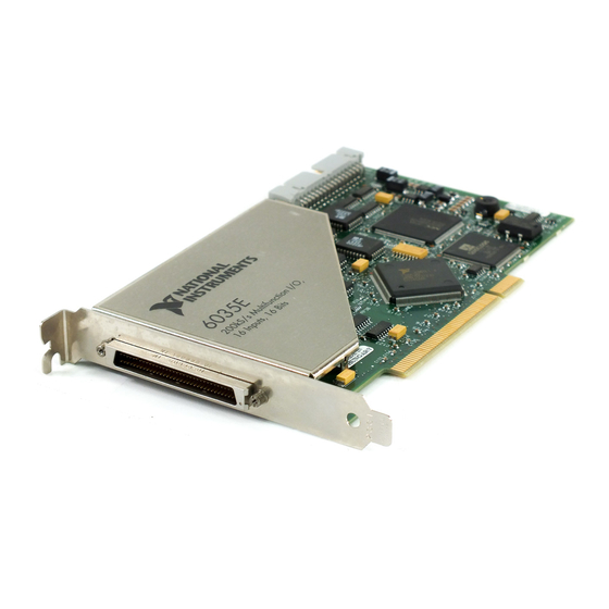
6034E/6035E
User Manual
Multifunction I/O Boards for
PCI, PXI, and CompactPCI Bus Computers
6034E/6035E User Manual
July 1999 Edition
Part Number 322339A-01
Table of
Contents
Previous
Page
Next
Page
1
2
3
4
5
Advertisement
Table of Contents
Need help?
Do you have a question about the 6034E and is the answer not in the manual?
Ask a question
Questions and answers
Related Manuals for National Instruments 6034E
I/O Systems National Instruments PXI-6040E User Manual
(265 pages)
PCI Card National Instruments 6035E User Manual
Daq multifunction i/o boards for pci, pxi, and compactpci bus computers (114 pages)
PCI Card National Instruments 6509 User Manual
(32 pages)
PCI Card National Instruments 6711 User Manual
Analog voltage output device for pci/pxi/compactpci/pcmcia/1394 bus computers (84 pages)
PCI Card National Instruments PXI-8360 Manual
(18 pages)
PCI Card National Instruments DAQ X Series User Manual
(299 pages)
PCI Card National Instruments NI PCIe-1429 Getting Started
(10 pages)
PCI Card National Instruments PCI-6509 User Manual
(27 pages)
PCI Card National Instruments PCIe-8375 Setting Up
Setting up your fiber-optic mxi -express x4 for pxi express (9 pages)
PCI Card National Instruments PXI-1409 Getting Started
(9 pages)
PCI Card National Instruments PXIe-8821 User Manual
(32 pages)
PCI Card National Instruments PXI Express PXIe-1073 User Manual
(42 pages)
PCI Card National Instruments IMAQ PCI-1409 User Manual
High-quality monochrome image acquisition boards for pci, pxi, and compactpci bus (55 pages)
PCI Card National Instruments IMAQ PCI-1407 User Manual
High-quality monochrome image acquisition boards for pci, pxi, and compactpci bus (51 pages)
PCI Card National Instruments PCI-8361 User Manual
(128 pages)
PCI Card National Instruments PCI-FBUS Installation Manual
Foundation fieldbus hardware and ni-fbus software (12 pages)
This manual is also suitable for:
6035e
Table of Contents
Print
Rename the bookmark
Delete bookmark?
Delete from my manuals?
Login
Sign In
OR
Sign in with Facebook
Sign in with Google
Upload manual
Upload from disk
Upload from URL


Need help?
Do you have a question about the 6034E and is the answer not in the manual?
Questions and answers