Denon DHT-391XP Service Manual
Hide thumbs
Also See for DHT-391XP:
- Specifications (2 pages) ,
- Owner's manual (68 pages) ,
- Owner's manual (68 pages)
Table of Contents
Advertisement
e
AVR-1311
AVR-391
DHT-1311XP
DHT-391XP
For purposes of improvement, specifi cations and design are subject to change without notice.
Please use this service manual with referring to the operating instructions without fail.
Some illustrations using in this service manual are slightly different from the actual set.
S0141-0V03DM/DG1010
SERVICE MANUAL
MODEL
AV SURROUND RECEIVER
MODEL
5.1CH HOME THEATER SYSTEM
Copyright 2010 D&M Holdings Inc. All rights reserved.
WARNING: Violators will be prosecuted to the maximum extent possible.
JP
E3
E3B
JP
E3
E3B
e
D&M Holdings Inc.
E2
EK
EA
E2
EK
EA
s
Ver. 3
Please refer to the
MODIFICATION NOTICE.
E1
E1C
E1
E1C
Advertisement
Table of Contents

Subscribe to Our Youtube Channel
Related Manuals for Denon DHT-391XP


Summary of Contents for Denon DHT-391XP
- Page 1 AVR-391 AV SURROUND RECEIVER MODEL DHT-1311XP DHT-391XP 5.1CH HOME THEATER SYSTEM For purposes of improvement, specifi cations and design are subject to change without notice. Please use this service manual with referring to the operating instructions without fail. Some illustrations using in this service manual are slightly different from the actual set.
-
Page 2: Safety Precautions
SAFETY PRECAUTIONS The following check should be performed for the continued protection of the customer and service technician. LEAKAGE CURRENT CHECK Before returning the unit to the customer, make sure you make either (1) a leakage current check or (2) a line to chassis resistance check. -
Page 3: Note For Schematic Diagram
NOTE FOR SCHEMATIC DIAGRAM WARNING: Parts marked with this symbol z have critical characteristics. Use ONLY replacement parts recommended by the manufacture CAUTION: Before returning the unit to the customer, make sure you make either (1) a leakage current check or (2) a line to chassis resistance check. If the leakage current exceeds 0.5 milliamps, or if the resistance from chassis to either side of the power cord is less than 460 kohms, the unit is defective. -
Page 4: System Configuration
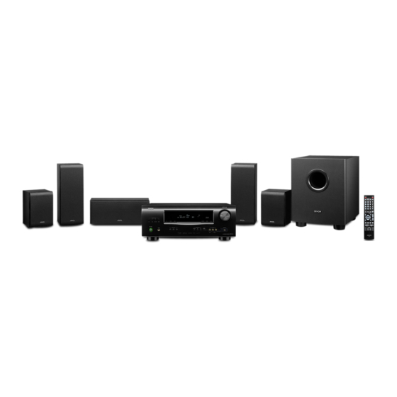
SYSTEM CONFIGURATION • AVR-1311 • DHT-1311XP (AVR-1311 + SYS-391HT) • AVR-391 • DHT-391XP (AVR-391 + SYS-391HT) SYS-391HT : Refer to page 104-113 for the service manual. SYS-391HT DSW-391 SC-F391(x2) SC-R391(x2) SC-C391 TECHNICAL SPECIFICATIONS n Audio Section n Tuner section –15 [FM](Note: μV at 75 Ω, 0 dBf = 1 x 10... - Page 5 DIMENSION 30.0 86.0 30.5 340.0 435.0 The illustration is AVR-1311 model.
-
Page 6: Caution In Servicing
When you update the fi rmware, you can use the following JIG (RS232C to internal connector conversion adapter with 4P FFC cable kit ). Please order to Denon Offi cial Service Distributor in your region if necessary. 8U-210100S WRITING KIT... - Page 7 DISASSEMBLY • Disassemble in order of the arrow of the fi gure of following fl ow. • In the case of the re-assembling, assemble it in order of the reverse of the following fl ow. • In the case of the re-assembling, observe "attention of assembling" it. •...
-
Page 8: Front Panel Assy
1. FRONT PANEL ASSY Proceeding : TOP COVER FRONT PANEL ASSY (1) Remove the screws. View from bottom (2) Cut the wire clamp band, then disconnect the connector wires and FFC cable. Remove the screws. FFC cable CN44 CN209 FRONT PANEL ASSY CN71 WIRE SUPPORT UNIT (3) Remove the screws. - Page 9 2. HDMI UNIT Proceeding : TOP COVER HDMI UNIT (1) Remove the screws. Direction of photograph: A (2) Disconnect the connector wire and FFC cable. HDMI UNIT FFC cable CN12...
-
Page 10: Input Unit
3. INPUT UNIT Proceeding : TOP COVER HDMI UNIT INPUT UNIT (1) Remove the screws. Direction of photograph: A (2) Disconnect the connector wires and FFC cables, then remove the screws. FFC cable CN71 CN43 CN42 INPUT UNIT FFC cable... -
Page 11: Radiator Assy
4. RADIATOR ASSY Proceeding : TOP COVER HDMI UNIT INPUT UNIT RADIATOR ASSY (1) Remove the screws. Direction of photograph: A (2) Disconnect the connector wires, then remove the screws. CN71 CN46 CN44 CN45 CN41 CN47 CN48 RADIATOR ASSY... -
Page 12: Power Unit
(3) Remove the RADIATOR ASSY from the main unit. Direction of photograph: C Please refer to "EXPLODED VIEW" for the disassembly method of each P.W.B included in RADIATOR ASSY. 5. POWER UNIT Proceeding : TOP COVER POWER UNIT Please refer to "EXPLODED VIEW" for the disassembly method of POWER UNIT. 6. -
Page 13: Special Mode
SPECIAL MODE Special mode setting button b Press the ON/STANDBY button to turn on while pressing both buttons A and B at the same time. Mode Button A Button B Contents Firmware versions such as Main, DSP are displayed in the FL μcom/DSP Version display mode STATUS DIMMER... -
Page 14: Error Display
1. μcom/DSP Version display mode 1.1. Operation specifi cations μcom/DSP version display mode: When started up, the version information is displayed. Starting up: With the "DIMMER" and "STATUS" buttons pressed, press the "ON/STANDBY" button to turn the power on. Now, press the "STATUS" button to the display the 2nd item information on the FL Display. 1.2. -
Page 15: About Replace The Microprocessor With A New One
ABOUT REPLACE THE MICROPROCESSOR WITH A NEW ONE When replaced of the U-PRO (Microprocessor) or the Flash ROM, confirm contents of the following. After PWB Name Ref. No. Description Remark replaced DIGITAL IC91 T5CN5 SOFTWARE: Main DIGITAL IC82 ST25VF080B-50-4C-S2AF SOFTWARE: DSP ROM After replaced A : Mask ROM (With software). -
Page 16: Update Firmware
2. UPDATE FIRMWARE Connect the update terminal of AV receiver with the “Writing Kit”. Set the switch of “Writing Kit" (Refer to the table below). DSPBOOT CNVSS Press the "ON/STANDBY" button to turn the power on of AV receiver. Set the switch of “Writing Kit" (Refer to the table below). DSPBOOT CNVSS Press the "RESET"... - Page 17 DSP SF1 Choose Ram File(OnBoard_M330.s32). Choose Ram File(OnBoard_M330.s32).
- Page 18 Choose Flash File(DSP : SF1). Choose "AVR1311_SF1_*_*_*_01.s32". Choose "Hex File (*.S32)".
- Page 19 (10) Click the “Start” button. The Setup Status bar appears.
- Page 20 (11) "Finished!!" is displayed. Click the "OK"” button. (12) Set the switch of “Writing Kit" (Refer to the table below). DSPBOOT CNVSS (13) Press the "RESET" switch of “Writing Kit". (14) AV receiver is power on and starts update of DSP1. (15) "Write Comleted"...
- Page 21 (19) Choose Flash File(DSP : SF2). Choose "AVR1311_SF2_*_*_*_01.s32". Choose "Hex File (*.S32)".
- Page 22 (20) Click the “Start” button. The Setup Status bar appears. (21) "Finished!!" is displayed. Click the "OK"” button.
- Page 23 (22) Set the switch of “Writing Kit" (Refer to the table below). DSPBOOT CNVSS (23) Press the "RESET" switch of “Writing Kit". (24) AV receiver is power on and starts update of DSP2. (25) "Write Comleted" is displayed in the FL tube. (26) Set the switch of “Writing Kit"...
- Page 24 (29) Choose Flash File(MAIN). Choose "AVR1311.s32". Choose "Hex File (*.S32)".
- Page 25 (30) Click the “Start” button. The Setup Status bar appears. (31) "Finished!!" is displayed. Click the "OK"” button.
- Page 26 (32) Set the switch of “Writing Kit" (Refer to the table below). DSPBOOT CNVSS (33) Press the "RESET" switch of “Writing Kit". (34) Initializing. 1. Turn off the power using ON/STANDBY button. 2. Press ON/STANDBY button while simultaneously pressing SURROUND MODE 0 and SURROUND MODE 1 buttons.
- Page 27 ADJUSTMENT Audio Section Idling Current Required measurement equipment: DC Voltmeter 1. Preparation (1) Avoid direct blow from an air conditioner or an electric fan, and adjust the unit at normal room temperature 15 °C ~ 30 °C. (2) Presetting • POWER (Power source switch) •...
-
Page 28: Surround Modes And Parameters
SURROUND MODES AND PARAMETERS... -
Page 32: Troubleshooting
TROUBLE SHOOTING 1. POWER 1.1. Power not turn on Power not turn on. Are there any incomplete connections in the Is there a short circuit Correct the short Is the ON/STANDBY indicator on the front panel connectors connecting between the speaker circuit between the fl... -
Page 33: Analog Video
2. Analog video MONITOR OUT(CVBS) Output NG Check ±5V The power supply circuitry is defective. +5V : C755 -5V : C754 Check output The IC71 and surrounding circuitry is defective. Output V : IC71-1pin Check cable between main unit and monitor or Check monitor. - Page 34 Check HDMI output setting, referring to the (5) Is the BD/DVD player's HDMI output setting correct? BD/DVD player's operating instructions. (6) When using a DENON BD/DVD player's, is the fl uorescent display tube's "HDMI" indicator lit? If using a non-DENON BD/ DVD player's, proceed to "YES".
- Page 35 HDMI connector for the input from the HDMI connector display's "HDMI" indicator lit? on the side on which the BD/DVD player is (JK11/JK12/JK13/JK14) If using a non-DENON BD/ connected. to the IC11 is defective. DVD player, proceed to Is communication waveform confi rmed in "NO".
- Page 36 (19) Check xtal oscillator. The X101 or IC11 is defective. Is there 28.6363MHz oscillation of X101? (20) Check RESET. Is RESET waveform confi rmed in IC11 (97pin), when power is The RESET pattern or IC11 is defective. turned on? (If continued to "H" or " L", proceed to "NO".) (21) Check control signal(I2C).
- Page 37 3.2. HDMI test point and waveforms Detail Detail TMDS D2+ TMDS D0+ TMDS D2- TMDS D0- TMDS D2- TMDS D0- TMDS D2+ TMDS D0+ TMDS D1+ TMDS CK+ TMDS D1- TMDS CK- TMDS D1+ TMDS D1+ TMDS D1- TMDS D1- Detail Detail 43pin DDC_DATA...
- Page 38 DDC_CLK/DDC_DATA/TMDS : Check item (15),(17) 0.9V DDC_CLK 2.48V TMDS SIGNAL DDC_DATA IPINDE/IPINVSYNC/IPINHSYNC/IPINPCK : Check item (21) HDMI_SDA HDMI_SCL...
-
Page 39: Clock Flow & Wave Form In Digital Block
CLOCK FLOW & WAVE FORM IN DIGITAL BLOCK Wave form CH1: D-DATA CH1: DATA CH2: fs CH3: 64fs CH1: DATA CH2: fs CH3: 64fs CH4: 256fs... -
Page 40: Block Diagram
BLOCK DIAGRAM... -
Page 44: Laevel Diagram
LAEVEL DIAGRAM... -
Page 46: Printed Wiring Boards
PRINTED WIRING BOARDS FRONT (COMPONENT SIDE) d HEADPHONE (COMPONENT SIDE) d REGULATOT (COMPONENT SIDE) d PHONE (COMPONENT SIDE) d Lead-free Solder When soldering, use the Lead-free Solder (Sn-Ag-Cu). - Page 47 FRONT (FOIL SIDE) d HEADPHONE (FOIL SIDE) d REGULATOT (FOIL SIDE) d PHONE (FOIL SIDE) d Lead-free Solder When soldering, use the Lead-free Solder (Sn-Ag-Cu).
- Page 48 VOLUME (COMPONENT SIDE) d AUX (COMPONENT SIDE) d POWER (COMPONENT SIDE) d VOLUME (FOIL SIDE) d AUX (FOIL SIDE) d POWER (FOIL SIDE) d Lead-free Solder When soldering, use the Lead-free Solder (Sn-Ag-Cu).
- Page 49 MAIN (COMPONENT SIDE) d Lead-free Solder When soldering, use the Lead-free Solder (Sn-Ag-Cu).
- Page 50 INPUT (COMPONENT SIDE) d Lead-free Solder When soldering, use the Lead- free Solder (Sn-Ag-Cu).
- Page 51 INPUT (FOIL SIDE) d Lead-free Solder When soldering, use the Lead- free Solder (Sn-Ag-Cu).
- Page 52 HDMI (COMPONENT SIDE) Lead-free Solder When soldering, use the Lead-free Solder (Sn-Ag-Cu).
- Page 53 HDMI (FOIL SIDE) Lead-free Solder When soldering, use the Lead-free Solder (Sn-Ag-Cu).
-
Page 54: Schematic Diagrams
SCHEMATIC DIAGRAMS (1/7) - Page 55 HDMI_MCLK HDMI_SCLK HDMI_LRCLK HDMI_SDATA3 HDMI_SDATA2 HDMI_MCLK R188 OPEN HDMI_SCLK HDMI_SDATA1 HDMI_LRCLK HDMI_SDATA0 HDMI_SDATA3 +5VH +5VH HDMI_SDATA2 Q107 HDMI_SPDIF HDMI_SDATA1 HDMI_SDATA0 Q108 YKF45-7074N R118 KRA102S OPEN R196 PWRDNB HP DET KRC103S HDMI_RESET R120 INT_TX C104 PWRDNB INT2 0.1uF R119 DDC DATA INT1 HDMI_RESET DDC CLK...
- Page 56 ANALOG AUDIO SIGNAL LINE SCHEMATIC DIAGRAMS (3/7)
- Page 57 VIDEO SIGINAL LINE COMPONENT (Y) SIGNAL LINE SCHEMATIC DIAGRAMS (4/7)
- Page 58 ANALOG AUDIO SIGNAL LINE DIGITAL AUDIO SIGINAL LINE SCHEMATIC DIAGRAMS (5/7)
- Page 59 SCHEMATIC DIAGRAMS (6/7)
- Page 60 ANALOG AUDIO SIGNAL LINE SCHEMATIC DIAGRAMS (7/7)
-
Page 61: Wiring Diagram
WIRING DIAGRAM... - Page 62 EXPLODED VIEW AVR1311 AVR1311 AVR391 AVR391 WARNING: Parts marked with this symbol have critical characteristics. Use ONLY replacement parts recommended by the manufacturer.
-
Page 63: Parts List Of Exploded View
PARTS LIST OF EXPLODED VIEW zParts for which "nsp" is indicated on this table cannot be supplied. zP.W.B. ASS'Y for which "nsp" is indicated on this table cannot be supplied. When repairing the P.W.B. ASS'Y, check the board parts table and order replacement parts. zPart indicated with the mark "... - Page 64 REAR PANEL 1311SPE1C CKF3A437Y REAR PANEL 391BKE3 CKF1A437Z REAR PANEL 391BKEA CKF1A437Y REAR PANEL 391BKE3B CKF1A437X 00D1310158007 DENON BADGE(BLACK049) CGB1A140U 00D1310158010 DENON BADGE(SILVER052) CGB1A140T FIP BRACKET CMD1A572 00M07BW257010 TOP CABINET CKC2A155K117 943403002040M TOP CABINET CKC1A155D11 HEAT SINK CMY8A161 TRANS BRACKET...
- Page 65 Ref.No. Part No. Part Name Remarks Q'ty SCREW CTW3+12JR SPECIAL SCREW CHD1A023R SCREW CTB3+8JFZR SCREW CTB3+8JFN SCREW CTBD3+8JFZR SCREW CTBD3+8JFN...
- Page 66 PACKING VIEW (for AVR-1311, 391) 8 9 10 PARTS LIST OF PACKING & ACCESSORIES (for AVR-1311, 391) zParts for which "nsp" is indicated on this table cannot be supplied. zPart indicated with the mark " " is not illustrated in the exploded view. zThe parts listed below are for maintenance only, might differ from the parts used in the unit in appearances or dimensions.
- Page 67 Ref.No. Part No. Part Name Remarks Q'ty 1311SPE2,1311BKE2, 00D9430113403 FM 1 POLE ANT. CSA1A018Z 1311SPE1C,391BKEA 90M-ZA000230R FM 1 POLANT(UL) 391BKE3 CSA1A019Z 943116009500S AM LOOP ANT CSA1A032Z POLY BAG CPB1061W 943531009950D OUTCARTON BOX 1311SPE2,1311BKE2 CPG1A924X 943531009960D OUTCARTON BOX 1311SPE1C CPG1A924V 943531009520D OUTCARTON BOX 391BKE3,391BKEA CPG1A924Z CONTROL LABEL...
- Page 68 PACKING VIEW (for DHT-1311XP, 391XP) 5-1 6 7 8 9 10 SYS-391HT (Refer to page 109,110.) PARTS LIST OF PACKING & ACCESSORIES (for DHT-1311XP, 391XP) zParts for which "nsp" is indicated on this table cannot be supplied. zPart indicated with the mark " "...
- Page 69 Ref.No. Part No. Part Name Remarks Q'ty 943533009940D SNOW PAD(R) CPS1A883 541110486002D INSTRUCTION MANUAL A 1311SPE2,1311BKE2 CQX1A1538Z 541110603005D INSTRUCTION MANUAL B 1311SPE2,1311BKE2 CQX1A1538Y 541110484006D INSTRUCTION MANUAL 391BKE3,391BKE3B CQX1A1537Z 541110489001D INSTRUCTION MANUAL 391BKEA CQX1A1541Z 307010085006D REMOCON TRANSMITER ASS'Y CARTAVR1311 BATTERY (SIZE 'AAA') CABR03PPB 00D9430113403 FM 1 POLE ANT.
- Page 70 PRELIMINARY SEMICONDUCTORS Only major semiconductors are shown, general semiconductors etc. are omitted to list. The semiconductor which described a detailed drawing in a schematic diagram are omitted to list. 1. IC's R2A15218FP (INPUT :IC61) AVCC MUTE AVCC N.C. AVEE AVEE N.C.
- Page 71 R2A15218FP Terminal Functions PIN No. Function Name 23,21, FROUT,FLOUT, 17,15, COUT,SWOUT, Output pin of FL/FR/C/SW/SL/SR/SBL/SBR channel 11,9, SROUT, SLOUT, SBROUT,SBLOUT 24,20, FRC,FLC, 18,14, CC,SWC, Connects capacitor for reducing click noise of 12,8, SRC,SLC, L/R/C/SW/SL/SR/SBL/SBR channel volume SBRC,SBLC 4,7,10,16, Analog ground of internal circuit AGND 19,22,56 28,34...
- Page 72 NJM2595M (INPUT : IC71) Vin1 Vin2 75Ω Vout1 Driver Vin3 75Ω Vout2 Vin4 Driver Vin5 75Ω Vout3 Driver NJM2586M (INPUT : IC73) CH1 OUT CH1 IN1 Driver Bias Cont1 Cont1 Cont2 CH2 OUT CH1 IN2 Driver Bias Cont1 CH3 OUT CH1 IN3 Driver Bias...
- Page 73 CS42528 (INPUT : IC84) CS42528 Block diagram...
- Page 74 CS42528 Terminal Functions...
- Page 75 CS497024CVZ (INPUT : IC81)
- Page 76 CS497024CVZ Block diagram M12L16161A5TG (INPUT : IC83)
- Page 77 TC74VHC157FT (INPUT : IC85) SELECT A S G T5CN5 (INPUT : IC91)
- Page 78 T5CN5 Terminal Functions...
- Page 79 ADV7622BSTZ (HDMI : IC11) DDCC_SCL 108 DDCA_SDA CVDD 107 RTERM CGND 106 5V_DETA RXC_C- 105 HP_CTRLA RXC_C+ 104 PGND TVDD 103 PVDD RXC_0- 102 XTAL1 RXC_0+ 101 XTAL CGND 100 PVDD RXC_1- 10 99 PGND RXC_1+ 11 98 PWRDNB TVDD 12 97 RESETB RXC_2- 13 96 MCLK_OUT...
- Page 80 ADV7622BSTZ Terminal Functions Location Mnemonic Type Description DDCC_SCL Digital Input HDCP slave serial clock port C. DDCC_SCL is a 3.3 V input that is 5 V tolerant. CVDD Power Receiver comparator supply voltage (1.8V) CGND Ground TVDD and CVDD Ground RXC_C- HDMI Input Digital input clock Complement of port C...
- Page 81 Location Mnemonic Type Description D in the HDMI interface. RXD_0+ HDMI Input Digital input channel 0 True of port D in the HDMI interface. CGND Ground TVDD and CVDD Ground RXD_1- HDMI Input Digital input channel 1 complement of port D in the HDMI interface.
- Page 82 Location Mnemonic Type Description TXGND Ground TXAVDD Ground TX0- HDMI Output Differential Output Channel 0 Complement. Differential output of the red data at 10× the pixel clock rate; supports TMDS logic level. TX0+ HDMI Output Differential Output Channel 0 True. Differential output of the red data at 10×...
- Page 83 Location Mnemonic Type Description N = 1, 2, 3, or 4. Set to 128 × sampling frequency (fs), 256 × fs, 384 × fs, or 512 × fs. Supports 1.8 V to 3.3 V CMOS logic levels. SCLK_IN Digital Input I2S Audio Clock.
- Page 84 Location Mnemonic Type Description AP0_OUT Digital Output Audio output port 0. AP1_OUT Digital Output Audio output port 1. AP2_OUT Digital Output Audio output port 2. AP3_OUT Digital Output Audio output port 3. AP4_OUT Digital Output Audio output port 4. DGND Ground Ground for DVDD DVDD...
- Page 85 Location Mnemonic Type Description RXA_C- HDMI Input Digital input clock Complement of port A in the HDMI interface. RXA_C+ HDMI Input Digital input clock True of port A in the HDMI interface. TVDD Power Receiver terminator supply voltage (3.3 V) RXA_0- HDMI Input Digital input channel 0 complement of port...
- Page 86 Location Mnemonic Type Description RXB_1+ HDMI Input Digital input channel 1 true of port B in the HDMI interface. TVDD Power Receiver terminator supply voltage (3.3 V) RXB_2- HDMI Input Digital input channel 2 complement of port B in the HDMI interface. RXB_2+ HDMI Input Digital input channel 2 true of port B in the...
-
Page 87: Pin Connection
2. FL DISPLAY FLD (18-ST-13GINK) (FRONT : U100) PIN CONNECTION GRID ASSIGNMENT... - Page 88 ANODE CONNECTION...
-
Page 89: Parts List Of P.w.b. Unit
PARTS LIST OF P.W.B. UNIT zParts for which "nsp" is indicated on this table cannot be supplied. zPart indicated with the mark " " is not illustrated in the exploded view. zThe parts listed below are for maintenance only, might differ from the parts used in the unit in appearances or dimensions. Note: The symbols in the column "Remarks"... - Page 90 Ref. No. Part No. Part Name Remarks Q'ty C211 CHIP CAP 0.1UF 50V K CCUS1H104KC C213 MYLAR CAP 0.1UF 50V J HCQI1H104JZT C214,215 943134010520S ELECT CAP 10UF 50V CCEA1HH100T C216 943134010530S ELECT CAP 1UF 50V CCEA1HH1R0T C217 943134010670S ELECT CAP 47UF 16V CCEA1CKS470T C218,219 943134010520S ELECT CAP 10UF 50V...
- Page 91 Ref. No. Part No. Part Name Remarks Q'ty CN207 LOCKINGTYPE STRAIGHTWAFER 2mm CJP05GI236ZW CN208 WAFER STRAIGHT CJP05GA19ZY CN209 WAFER ANGLE(2.5mm) CJP05GB03ZY z F201 943652000620S FUSE(0.1A 372SERIES/TR5) CBA2D0100A3EYT FL201 943172010110S VFD HCA-18SM01T CFLHCA18SM01T GND21,22 PCB BRACKET CMD1A569 JK201 90M-YT004310R JACK BOARD(3P) CJJ4S041Z JK202 943643010130S JACK...
-
Page 92: Main P.w.b. Unit Ass'y
MAIN P.W.B. UNIT ASS'Y Ref. No. Part No. Part Name Remarks Q'ty SEMICONDUCTORS GROUP IC41 00D2630641002 REGULATOR IC NJM7912FA HVINJM7912FA IC42 00D2630801004 REGULATOR IC NJM7812FA HVINJM7812FA IC45 00D2631162014 REGULATOR IC KIA78R05PI HVIKIA78R05PI IC46 231010031706S REGULATOR IC KIA278R05PI HVIKIA278R05PI Q401 00MHT800931A0 TR KTC3200GR HVTKTC3200GRT Q402,403 00D9430154200 TR KRA102M... - Page 93 Ref. No. Part No. Part Name Remarks Q'ty ZD41 943202010070S DIODE ZJ12B CVDZJ12BT ZD48 943202010080S DIODE ZJ5.1B CVDZJ5.1BT ZD49 90M-HD302440R DIODE ZJ4.7B CVDZJ4.7BT ZD51-60 90M-HD302390R DIODE ZJ3.3B CVDZJ3.3BT RESISTORS GROUP R494-501 METAL OXIDE FILM RES(4.7KOHM 5% 1W) KRG1SANJ4R7RT R502 METAL OXID EFILM RES(120OHM 1W J) KRG1SANJ121RT R505-514 METAL OXIDE FILMRES 2W...
- Page 94 Ref. No. Part No. Part Name Remarks Q'ty C423-426 CERAMIC CAP 33PF 50V J CCCT1H330JC C427 943134010660S ELECT CAP 470UF 6.3V CCEA0JH471T C428 943134010490S ELECT CAP 100UF 10V CCEA1AH101T C429-431 MYLAR CAP 0.01UF 100V J 1311E2 HCQI1H103JZT 1311E1C,391E3, C429-431 MYLAR CAP 1000PF 100V J MYLAR HCQI1H102JZT 391E3B,391EA C432...
-
Page 95: Fuse Holder
Ref. No. Part No. Part Name Remarks Q'ty C504 943134010600S ELECT CAP 3300UF 16V CCEA1CH332E C505 943134010680S ELECT CAP 47UF 50V CCEA1HH470T C508 943134010520S ELECT CAP 10UF 50V CCEA1HH100T C559 943134010470S ELECT CAP 0.1UF 50V CCEA1HH0R1T C561 943134010530S ELECT CAP 1UF 50V CCEA1HH1R0T C563,564 943134010470S ELECT CAP 0.1UF 50V... -
Page 96: Input P.w.b. Unit Ass'y
INPUT P.W.B. UNIT ASS'Y Ref. No. Part No. Part Name Remarks Q'ty SEMICONDUCTORS GROUP IC60 943231010390S REGULATOR IC KIA7805BPI CVIKIA7805BPI IC61 943235003810S IC R2A15218FP CVIR2A15218FP IC62-65 00D2631289900 IC AZ4580MTR-E1 CVIAZ4580MTR-E1 IC66,67 00D2630934900 IC BA4510F HVIBA4510F IC68 943231010390S REGULATOR IC KIA7805BPI CVIKIA7805BPI NOTE : IC69... - Page 97 Ref. No. Part No. Part Name Remarks Q'ty RN61 CHIP RES(100OHM 5% 1608X4) CRJ104DJ101T RN80 CHIP RES(33OHM 5%,1608X4) CRJ104DJ330T RN81,82 CHIP RES(10KOHM 5% 1608X4) CRJ104DJ103T RN83-90 CHIP RES(33OHM 5% 1608X4) CRJ104DJ330T RN91,92 CHIP RES(100OHM 5% 1608X4) CRJ104DJ101T RN93 CHIP RES(10KOHM 5% 1608X4) CRJ104DJ103T CAPACITORS GROUP C603,604...
- Page 98 Ref. No. Part No. Part Name Remarks Q'ty C696,697 943134010610S ELECT CAP 4.7UF 50V CCEA1HH4R7T C698 CHIP CAP 0.1UF 50V CCUS1H104KC C701-704 CHIP CAP 1500PF 50VK CCUS1H152KC C705,706 CHIP CAP 330PF 50V J CCUS1H331JA C707,708 CHIP CAP 1500PF 50VK CCUS1H152KC C709 CHIP CAP 0.1UF 50V CCUS1H104KC...
- Page 99 Ref. No. Part No. Part Name Remarks Q'ty C808 943134010610S ELECT CAP 4.7UF 50V CCEA1HH4R7T C809 CHIP CAP 0.1UF 50V CCUS1H104KC C810 943134010490S ELECT CAP 100UF 10V CCEA1AH101T C811 943134010630S ELECT CAP 470UF 10V CCEA1AH471T C812 CHIP CAP 0.1UF 50V CCUS1H104KC C813 CHIP CAP 1000PF 50V...
- Page 100 Ref. No. Part No. Part Name Remarks Q'ty C940,941 CHIP CAP 1000PF 50V CCUS1H102KC C946-953 CHIP CAP 1000PF 50V CCUS1H102KC C954 CHIP CAP 0.015UF 50V CCUS1H153KC C955 CHIP CAP 1UF 10V CCUS1A105KC C956 CHIP CAP 0.1UF 50V CCUS1H104KC C957 943134010530S ELECT CAP 1UF 50V CCEA1HH1R0T C958-961 CHIP CAP 0.1UF 50V...
- Page 101 Ref. No. Part No. Part Name Remarks Q'ty TU61 943183010310S TUNER(EUR)FM,AM,RDS(S/LAB) 1311E2,1311E1C,391EA CNVMW104MV1S63SN TU61 943183010320S TUNER(USA)FM(SCREW:FTYPE),AM(S/LAB) 391E3,391E3B CNVMW004MV1S63SA X801 943141010360S CRYSTAL 24.576MHz 15PF 30PPM HOX24576E150TF X901 943141010370S CRYSTAL 10.000MHz 22PF 30PPM HOX10000E220TF...
- Page 102 HDM P.W.B. UNIT ASS'Y Ref. No. Part No. Part Name Remarks Q'ty SEMICONDUCTORS GROUP IC11 943236010380S IC ADV7622BSTZ CVIADV7622BSTZ IC15 943239010400S REGULATOR IC NJM2845DL133 CVINJM2845DL133 IC16 IC EX3AV CVIEX3AV Q101 00D2690184907 CHIP TR KRA102S HVTKRA102S Q102 90M-BA001620R CHIP TR KRC103S CVTKRC103S Q103 00D2690184907 CHIP TR KRA102S...
- Page 103 Ref. No. Part No. Part Name Remarks Q'ty C178 CHIP CAP 0.015UF 25V CCUI1E153KC C179 CHIP CAP 15PF 50V CCUI1H150JA OTHERS PARTS GROUP BK11,12 PCB BRACKET CMD1A569 CN12 WAFER SMD(2MMPITCH) CJP05GA208ZY CN8B WAFER CJP19GA115ZY JK11-15 644010108608S HDMI JACK(SMD) CJJ9H010Z L101-108 CHIP FERRITE BEAD(60ohm 1608) CLZ9R005Z L109...
-
Page 104: Speaker System Pack
SYS-391HT section SPEAKER SYSTEM PACK TECHNICAL SPECIFICATIONS n Front speaker (SC-F391) n Surround speaker (SC-R391) Type: 2-way, 3-speakers Type: Full-range, 1-speaker Closed box / Low-leakage-fl ux Closed box Drive units: 8 cm cone bass-mid x 2 Drive units: 8 cm cone full range x 1 2.5 cm high range x 1 Input impedance: 6 Ω... -
Page 105: Speaker Ass'y
SC-F391 EXPLODED VIEW SC-F391 PARTS LIST OF EXPLODED VIEW Parts for which "nsp" is indicated on this table cannot be supplied. The parts listed below are for maintenance only, might differ from the parts used in the unit in appearances or dimensions. Ref. - Page 106 SC-R391 EXPLODED VIEW SC-R391 PARTS LIST OF EXPLODED VIEW Parts for which "nsp" is indicated on this table cannot be supplied. The parts listed below are for maintenance only, might differ from the parts used in the unit in appearances or dimensions. Ref.
- Page 107 SC-C391 EXPLODED VIEW SC-C391 PARTS LIST OF EXPLODED VIEW Parts for which "nsp" is indicated on this table cannot be supplied. The parts listed below are for maintenance only, might differ from the parts used in the unit in appearances or dimensions. Ref.
-
Page 108: Exploded View
DSW-391 EXPLODED VIEW DSW-391 PARTS LIST OF EXPLODED VIEW Parts for which "nsp" is indicated on this table cannot be supplied. The parts listed below are for maintenance only, might differ from the parts used in the unit in appearances or dimensions. Note: The symbols in the column "Remarks"... - Page 109 SYS-391HT PACKING VIEW...
- Page 110 SYS-391HT PARTS LIST OF PACKING VIEW Parts for which "nsp" is indicated on this table cannot be supplied. The parts listed below are for maintenance only, might differ from the parts used in the unit in appearances or dimensions. Note: The symbols in the column "Remarks" indicate the following destinations. E3B : Brazil model s E3 : U.S.A.
- Page 111 SCHEMATIC DIAGRAMS (1/1)
Need help?
Do you have a question about the DHT-391XP and is the answer not in the manual?
Questions and answers