
Subscribe to Our Youtube Channel
Related Manuals for Arcam AVR400


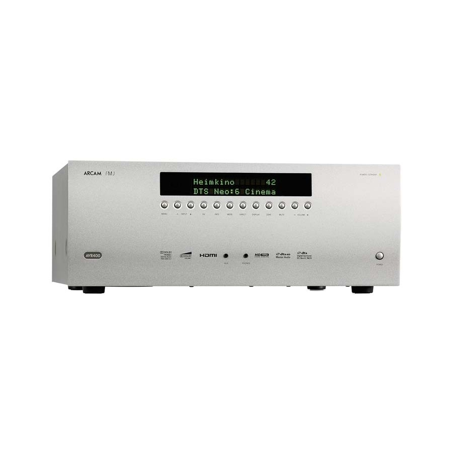
Summary of Contents for Arcam AVR400
- Page 1 AVR400 Service Manual Issue 1...
- Page 2 ECO NR. DATE CHG. ZONE DESCRIPTION OF CHANGE REL. DR. CHK. ITEM NO. PART No. DESCRIPTION TGP3523 / TGP3524 FASCIA ASSEMBLY BLACK / SILVER TGP3526 / TGP3527 COVER BLACK / SILVER HA4V06S TORX SCREW M4 x 6 23425 DRAWN BY: 7-9-2010 DATE: A &...
- Page 3 ECO NR. DATE CHG. ZONE DESCRIPTION OF CHANGE REL. DR. CHK. ITEM NO. PART No. DESCRIPTION TGP3539 TRANSFORMER - POWER FAN 80 x 80 x 25mm FAN MOUNTING BRACKET 23425 DRAWN BY: 7-9-2010 DATE: A & R CAMBRIDGE LTD ALL DIMENSIONS IN TOLERANCES UNLESS 0.00±...
- Page 4 ECO NR. DATE CHG. ZONE DESCRIPTION OF CHANGE REL. DR. CHK. SOLDERED TO POWER AMP PCB ITEM NO. PART No. DESCRIPTION TGP3534 CHASSIS ASSY TGP3535 FRONT PCB ASSY TGP3538 POWER AMP PCB ASSY TGP3525 FOOT ASSY TGP3540 TRANSFORMER - STANDBY 23425 DRAWN BY: 7-9-2010...
- Page 5 ECO NR. DATE CHG. ZONE DESCRIPTION OF CHANGE REL. DR. CHK. ITEM NO. PART No. DESCRIPTION TGP3528 REAR PANEL ASSY TGP3536 INPUT PCB ASSY - MAIN TGP3536 (part) INPUT PCB ASSY - ETHERNET TGP3536 (part) INPUT PCB ASSY - CONNECTORS TGP3537 HDMI PCB ASSY - MAIN TGP3537 (part)
- Page 6 AVR400 Power Amplifier Circuit Description Apart from the power transformer, the power amplifier electronics is fully contained on the large double sided PTH PCB and heatsink located at the bottom of the AVR400. This is called the Main Board on the schematic diagrams (pages 11 and 12). The Main Board also contains the mains input circuitry, in- cluding the safety fuses and standby power transformer, so great care should be exercised when probing this area of the board.
- Page 7 additional feedback further reduces high frequency distortion and crossover distortion within the audio band. These stages are partially decoupled from the Vcc and Vee power supplies by D5130/R5130/C5130 and D5129/R5129/C5129 respectively. They are also bootstrapped to the amplifier output via the networks R5118/C5128/R5128 and R5117/C5127/R5127.
- Page 8 1) Any amplifier channel pulls current through the SOA_PROTECT line for long enough to charge up capacitors C5871 and then C5872 so that Q5874 turns on. 2) Any amplifier channel pulls current through the OVERLOAD line for long enough to charge up C5882 and turn on Q5882 and thus Q5884.
- Page 9 Two secondary windings from the toroidal power transformer are fed in via CN63. Pins 1, 2 and 3 con- nect to a centre-tapped secondary winding used to generate approx +/- 20VDC via the bridge rectifier diodes D603/3/4/5 and the 2,200μF 35V reservoir capacitors C609 and C610. R603 and R604 are 0.47R 1W fusible resistors for circuit protection –...
- Page 10 It communicates with the Input Board via CN101 and a 31 way ribbon cable. Other connectors comprise CN94 which connects to two secondaries of the main power transformer and the hard wired BN93 which connects up the daughter board. There are two associated break off boards. One houses the front panel mounted single pole mains switch plus its suppression capacitor C901 and a connector BN502.
- Page 11 the same manner as described above for RL902) then the L front input is routed to the low noise micro- phone amplifier IC903. This operates as two cascaded virtual earth amplifiers, each with a voltage gain of approximately 21 (R961/960 and then R965/962). Note the MIC line is biased at +6V via resistors R956, R957 and R958.
- Page 12 IC101 has one 8 channel variable level output bus labelled VOL01 through to VOL08. Capacitors C295-8 and C231-4 float the ground ends of the associated internal potentiometers to minimize clicks This bus goes via specially selected 100μF/25V capacitors to the dual op amps IC121-124, wired as voltage follow- ers and running from the +/- 15V supplies.
- Page 13 IC143 is the Cirrus Logic CS42548. It includes an SPDIF receiver, 2 channel ADC and 8 channel DAC. Only one input (pin 43) of the SPDIF receiver is used; the others are grounded. IC143 has +5V analogue supplies, locally decoupled to analogue ground by C721/722 for VA (pin 24) and C703/704 for VARX (pin 41).
- Page 14 IC141 also has two sets of I2S data outputs. DA1 is an 8 channel I2S signal (pins 47, 48, 49 and 51) shown as part of the bus DA0(04:07). This feeds the input of the second DSP IC142 (on pins 23, 24, 26 and 27). The system clock is on pin 52 of IC141 and the LR clock on pin 54.
- Page 15 It contains two 9 way D-type board mounted plugs JK71 and JK72. JK71 is for RS232 control of the AVR400. JK72 is used to control an iPod or iPhone via an Arcam rDock or rLead (the latter also supports iPads).
- Page 16 the necessary level shifting. IC73 includes internal charge pumps to convert CMOS logic level inputs to +/-5V RS232 level outputs and +/-25V tolerant RS232 inputs to CMOS logic level outputs. Maximum rated speed is 300kb/sec. JK73 is a dual mono 3.5mm jack socket providing two +12V trigger outputs Z_1 and Z_2. The series pass transistors Q712/715 are pnp T0-92 types with emitters referred to the +12V rail via the paralleled 4.7R resistors R714/715 and R711/712.
- Page 17 The HDMI input SOC, IC901, is a 144 pin LQFP Analog Devices ADV3014B. This is a 4 into 1 HDMI 1.4a multiplexer and is connected to inputs 4 and 5 (VCR and PVR) on the rear panel (JK95 and JK96). The other two inputs on IC901 are not used.
- Page 18 Q914 and Q915 (on the underside of the PCB) send BYPASS_ON and BYPASS_OFF logic signals from IC906 to the array of 4 x 20-bit non-inverting line driver/bμFfers with tri-statable outputs, IC911/912 and IC915/916. These are arranged as a 40 way 2-in, 1-out fast switch to bypass IC906 when required (e.g. if 3D video is present).
- Page 19 AVR400 Analogue Video Board This is connected into the rest of the system via the HDMI board using CN301.The circuitry is shown on sheet 13 of the schematic diagram. The purposes of this PCB are: (1) to switch between the various analogue video inputs (comprising 4 each composite and s-video and 3 component video) (2) to route the chosen video signal to the HDMI board for processing (3) to provide one set of zone 1 video component video outputs...
- Page 20 FROM POWER TRANS CN94 FRONT CUP12326Z-1 M_GND R903 FIP91 CFLHCA16S202T C953 OPEN JW901 R977 OPEN M_GND OPEN D908 R904 M_GND OPEN CHGND 2010.04.12 D909 OPEN C903 : 47uF/50V -> 47uF/25V M_GND M_GND M_GND R909 Q901 C1027Y 2010.04.12 RC901 C903 : 100uF/63V -> 47uF/63V 2EA R906 C915 0.1uF...
- Page 25 CUP12328Z ADV7844 Worst Measured Currents ADV3014 Decoupling Capacitor 1.8V Total : 904.33mA DVDD_1V8_3014 PVDD_1V8_3014 TXAVDD_1V8_3014 CVDD_1V8_3014 Worst Measured Currents Worst Measured Currents Worst Measured Currents 3.3V Total : 240.3mA Worst Measured Currents +1.8VH2 L805 390mA L808 35mA L807 22.7mA +1.8VH2 L803 428mA +1.8VH2...
- Page 26 CUP12328Z Worst Measured Currents 250mA(20%:290mA) +2.5V_DVDDIO_SDRAM DVDDIO_3.3V +2.5V_DVDDIO_SDRAM IC904 Worst Measured Currents +2.5V_DVDDIO_SDRAM DDR_VREF Worst Measured Currents AVDD_1.8V Worst Measured Currents 100mA(20%:120mA) CVIA3S56D40FTPG5 190mA(20%:228mA) 240mA(20%:288mA) L811 0.1uF / 16V L814 +3.3VH2 L813 +2.5VH2 R669 33ohm (1005SIZE X 4),1/16W 33ohm (1005SIZE X 4),1/16W +1.8VH2 C231 9R005Z...
- Page 27 Worst Measured Currents Worst Measured Currents Worst Measured Currents 11mA(Max:12mA) 9.8mA(Max:10.5mA) L822 Worst Measured Currents Worst Measured Currents L827 Worst Measured Currents Worst Measured Currents 385mA(Max:412mA) +1.8VH1 1850mA(Max:1925mA) +1.8V_CORE +3.3VH1 L826 24mA(Max:24mA) +3.3V_IO +3.3VH1 L821 +3.3V_LBADC +2.5VH1 +2.5V_DDR +3.3VH1 L825 +3.3V_LVDS_PLL +3.3VH1 L820...
- Page 28 CUP12328Z 3.3V_TTL_MUX1 +3.3VH2 3.3V_TTL_MUX +3.3VH2 L835 L844 Option 1000P_NC C543 1000P_NC Option +3.3VH2 C544 INPUT OUTPUT HDMI By Pass Mode Interface Scaling Mode Interface 3.3V_TTL_MUX 3.3V_TTL_MUX1 +1.8VH2 BYPASS_ON BYPASS_OFF IC912 74ALVCH16827DGG IC915 74ALVCH16827DGG 33ohm (1005SIZE X 4),1/16W 33ohm (1005SIZE X 4),1/16W 1OE2 1OE1 1OE2...
- Page 29 CUP12328Z DC/DC REGUALTOR TO VIDEO V-GND +15VA -15VA IC930 OSD_H SV_Y_THRU DDRMEM_REG_ 2.5V SV_C_THRU CVBS_THRU +1.8VH1 COM_Y_THRU PW_GND PW_GND PW_GND 2.5V IC922 COM_PB_THRU COM_PR_THRU +15V_DC/DC L858 10UH/3A +3.3VDD +2.5VH1 COM_Y_CONV C551 COM_PB_CONV L855 COM_PR_CONV 0.01uF 1321_SCL 1321_SDA OSD_SDA OSD_SCL OSD_CE CVBS_CONV 2.5V IC929...
-
Page 30: Schematic Diagram
FROM POWER BOARD CN501 BN591 +12V +12V GND_DEC SBL_OUT SUB_POWER *CHG1A502 : Rubber Damping Pad 15 X 6 X 3mm RY51 *CHG1A503 : Rubber Damping Pad 7.5 X 6 X 3mm R5128 R5130 D5130 FAN_12V JK51 *CHG1A504: 3M Bumpon SJ-6344 68(F) 0.25W 22 0.5W(Fusible) 1N5819... -
Page 31: Schematic Diagram
D5630 D5430 R5628 R5630 R5428 R5430 68(F) 0.25W 22 0.5W(Fusible) 68(F) 0.25W 22 0.5W(Fusible) 1N5819 1N5819 Q5412 Q5612 BC856B BC856B C5650 Q5603 Q5604 R5612 Q5403 Q5404 R5412 GND_DEC C5450 BC856B GND_DEC BC856B (N.F) BC856B BC856B 1K(F) 1K(F) (N.F) Q5615 Q5470 Q5670 Q5415 NJL3281DG... - Page 32 VIDEO PART JK85 CJJ4M069Z(GOLD) C770 Z2 OUT 470/10V R825 VGND VGND L801 * LC74763M OPTION TABLE +5VV 100UH C806 0.01uF C871 C872 X801 X802 IC83 IC83 LC74763M LC74763M +5VV C827 17.734 14.318 1/50V 0.01uF C805 VGND VGND VGND NTSC 14.318 VDD1 VGND R871...
- Page 33 POWER PART RS232 PART +15V -15V +5VD L653 IC68 L654 CLZ9Z014Z HVINJM2391DL133 CLZ9Z014Z +12V +15V CN61 MGND +15VD D742 -15V +15VD +5VD R742 +5VD +15VD +5VD Q643 ST+5V C742 0.1uF CVTD44H11GVA +5VD TO HDMI MGND +5VD TO INPUT DGND Q712 KTA1266 R716 R649 +5VD...
- Page 34 SCREW MARK DGND REVISION SCHEMATIC DIAGRAM SHEET AVR400 MODEL DESIGN CHECK APPROVE DRAWING NO 2330SCDZ L.J.Y L.J.H S.H.S (VIDEO) 10.11.17 10.11.17 10.11.17...
Need help?
Do you have a question about the AVR400 and is the answer not in the manual?
Questions and answers