Table of Contents
Advertisement
Quick Links
Advertisement
Table of Contents

Related Manuals for Arcam AVR360


Summary of Contents for Arcam AVR360
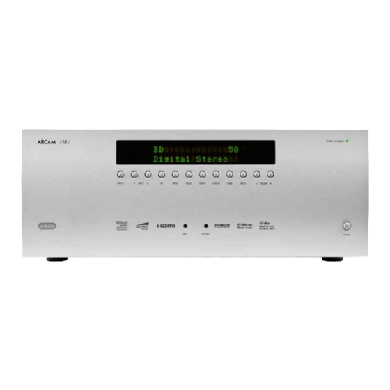
- Page 1 AVR360 Service Manual Issue 1...
-
Page 2: Table Of Contents
Exploded drawing — amplifier PCB and rear panel .................5 Exploded drawing — Input (preamp), RS232, analogue video & digital video PCBs ..6 AVR360 Power Amplifier Circuit Description ..................7 AVR360 Main Power Supplies Circuit Description ................9 AVR360 Front Panel Board Circuit Description ...................11 AVR360 Input Board Circuit Description ....................12 Analogue inputs, volume control and outputs ..................12... -
Page 3: Exploded Drawing - Cover And Fascia Removal
TOLERANCES UNLESS 0.00± 0.10 CHECKED BY: OTHERWISE STATED 0.0 ± 0.20 MILLIMETERS UNLESS ANGULAR TOL. +2 DEGREES OTHERWISE STATED ORIGINAL SCALE 1:4 MATERIAL: FINISH: SHT 1 OF 4 PART NUMBER AND DRAWING NUMBER AVR360 MAIN ASSEMBLY DRAWING TITLE COVER + FASCIA... -
Page 4: Exploded Drawing - Main Transformer And Fans
TOLERANCES UNLESS 0.00± 0.10 CHECKED BY: OTHERWISE STATED 0.0 ± 0.20 MILLIMETERS UNLESS ANGULAR TOL. +2 DEGREES OTHERWISE STATED ORIGINAL SCALE 1:4 MATERIAL: FINISH: SHT 2 OF 4 PART NUMBER AND DRAWING NUMBER AVR360 MAIN ASSEMBLY DRAWING TITLE FANS + TRANSFORMER... -
Page 5: Exploded Drawing - Amplifier Pcb And Rear Panel
TOLERANCES UNLESS 0.00± 0.10 CHECKED BY: OTHERWISE STATED 0.0 ± 0.20 MILLIMETERS UNLESS ANGULAR TOL. +2 DEGREES OTHERWISE STATED ORIGINAL SCALE 1:4 MATERIAL: FINISH: SHT 3 OF 4 PART NUMBER AND DRAWING NUMBER AVR360 MAIN ASSEMBLY DRAWING TITLE POWER PCBs + FEET... -
Page 6: Exploded Drawing - Input (Preamp), Rs232, Analogue Video & Digital Video Pcbs
TOLERANCES UNLESS 0.00± 0.10 CHECKED BY: OTHERWISE STATED 0.0 ± 0.20 MILLIMETERS UNLESS ANGULAR TOL. +2 DEGREES OTHERWISE STATED ORIGINAL SCALE 1:2.5 MATERIAL: FINISH: SHT 4 OF 4 PART NUMBER AND DRAWING NUMBER AVR360 MAIN ASSEMBLY DRAWING TITLE REAR PANEL + PCBs... -
Page 7: Avr360 Power Amplifier Circuit Description
Apart from the power transformer, the power amplifier electronics is fully contained on the large double sided PTH PCB and heatsink located at the bottom of the AVR360. This is called the Main Board on the schematic diagrams (pages 11 and 12). The Main Board also contains the mains input circuitry, in- cluding the safety fuses and standby power transformer, so great care should be exercised when probing this area of the board. - Page 8 R5175, using the 2 pin connector CN51, 5 minutes or more after the AVR360 is powered up. The power amplifier output is routed across the PCB to the back panel. It includes a Zobel network (sometimes called a Boucherot cell) R5183/C5183 and a series inductor L5185 damped by a 4.7R 2W re-...
-
Page 9: Avr360 Main Power Supplies Circuit Description
Considering the Main Board first, the power supply voltage is fixed depending on which regional vari- ant the AVR360 is (US or EU). The mains voltage is fixed to a nominal settings of 115V (US) or 230V (EU) +/- 15%. The 20mm fuse in line with the frame transformer is rated at 15A T (Time delay) for 115V units and at 8A T for 230V units. - Page 10 Now consider the Power Supply Board, found on page 14 of the schematic. This generates all the main DC supplies for the AVR360 except +Vcc and -Vee for the power amplifiers and the non-logic part of the VFD display requirements of the Front Panel Board. Note that additional local regulation also takes place on the other PCBs, e.g.
-
Page 11: Avr360 Front Panel Board Circuit Description
IR remote control. It is designed to work with the 36-38kHz carrier frequencies associated with the Philips RC5 protocol. Note that it operates from the ST+5V rail to enable the AVR360 to be woken up. It does not demodulate the IR – this is done by the system microprocessor. -
Page 12: Avr360 Input Board Circuit Description
R957 and R958. The amplified signal is output to the Input Board on pin 5 of CON101. AVR360 Input Board Circuit Description The Input Board comprises a 4 layer PCB; this is attached directly to the back panel via its various sock- ets and to the heatsink by two steel brackets. -
Page 13: Spdif Inputs, Adcs, Dacs And Audio Dsps
IC101 has a fixed level stereo output for Zone 2 (SUB_L and SUB_R) and a second one, adjustable from 0dB to -18dB in 6dB steps, for the AVR360’s analogue to digital converter (ADC_L and ADC_R). IC101 has one 8 channel variable level output bus labelled VOL01 through to VOL08. Capacitors C295-8 and C231-4 float the ground ends of the associated internal potentiometers to minimize clicks This bus goes via specially selected 100μF/25V capacitors to the dual op amps IC121-124, wired as voltage follow-... - Page 14 Each of the 4 coaxial inputs is buffered by two NOR gates, contained in IC159 and IC160, before being switched by one half of the dual 4 input multiplexer IC147. The output on pin 7 is then sent to the 8 input multiplexer IC140.
-
Page 15: System Control Microprocessors
IC155 is a MOSFET switch to enable the HDMI CEC (Consumer Electronic Control) bus when the unit is powered up, and to isolate the parts of the bus external to the AVR360 when it is powered down. IC151 has several sets of comms busses - SPI, I2C and UARTs - depending on which system or peripheral ICs are being addressed. - Page 16 Australia, Canada, Korea and other Digital Radio markets. It also supports USB2, and Ethernet up to 100 Mb/s, enabling the AVR360 to be a network audio client. A spare copy of the AVR360’s unique MAC (Media Access Controller) address can be found on the screening can of the Venice 6.2 module. Its FM radio function is not used.
-
Page 17: Avr360 Rs232 Board
It contains two 9 way D-type board mounted plugs JK71 and JK72. JK71 is for RS232 control of the AVR360. JK72 is used to control an iPod or iPhone via an Arcam rDock or rLead (the latter also supports iPads). - Page 18 The video processor IC906 is an ST (formerly Genesis) “Torino” type FLI30336AC in a large 416 pin BGA package. It is used to de-interlace and scale all the AVR360’s video inputs to the required output resolution(s) up to 1080p and also to generate the system OSD (on screen display). Note that IC906’s...
- Page 19 In the AVR360’s implementation the HDMI audio output is limited to stereo rather then 8 channels – via I2S0 (pin 12), plus MCLK (pin 11), SCLK (pin16) and LRCLK (pin 17). SPDIF from the AVR360 is input to pin The ARC signal, if received from a downstream sink such as a TV, is output from pin 46 of IC918 and sent via back to the input board.
-
Page 20: Avr360 Analogue Video Board
The outputs go to the analogue video daughter board via the 30 way socket BN301. Note that the composite and s-video outputs are not actually used in the AVR360 so are not wired beyond CN301 on the daughter board. The Y, Cr, Cb component video outputs are terminated with 75 ohm series resistors on the Analogue Video daughter board described next. -
Page 25: Hdmi Pcb Schematics
CUP12328Z ADV7844 Worst Measured Currents ADV3014 Decoupling Capacitor 1.8V Total : 904.33mA DVDD_1V8_3014 PVDD_1V8_3014 TXAVDD_1V8_3014 CVDD_1V8_3014 Worst Measured Currents Worst Measured Currents Worst Measured Currents 3.3V Total : 240.3mA Worst Measured Currents +1.8VH2 L805 390mA L808 35mA L807 22.7mA +1.8VH2 L803 428mA +1.8VH2... - Page 26 CUP12328Z Worst Measured Currents 250mA(20%:290mA) +2.5V_DVDDIO_SDRAM DVDDIO_3.3V +2.5V_DVDDIO_SDRAM IC904 Worst Measured Currents +2.5V_DVDDIO_SDRAM DDR_VREF Worst Measured Currents AVDD_1.8V Worst Measured Currents 100mA(20%:120mA) CVIA3S56D40FTPG5 190mA(20%:228mA) 240mA(20%:288mA) L811 0.1uF / 16V L814 +3.3VH2 L813 +2.5VH2 R669 33ohm (1005SIZE X 4),1/16W 33ohm (1005SIZE X 4),1/16W +1.8VH2 C231 9R005Z...
- Page 27 Worst Measured Currents Worst Measured Currents Worst Measured Currents 11mA(Max:12mA) 9.8mA(Max:10.5mA) L822 Worst Measured Currents Worst Measured Currents L827 Worst Measured Currents Worst Measured Currents 385mA(Max:412mA) +1.8VH1 1850mA(Max:1925mA) +1.8V_CORE +3.3VH1 L826 24mA(Max:24mA) +3.3V_IO +3.3VH1 L821 +3.3V_LBADC +2.5VH1 +2.5V_DDR +3.3VH1 L825 +3.3V_LVDS_PLL +3.3VH1 L820...
- Page 28 CUP12328Z 3.3V_TTL_MUX1 +3.3VH2 3.3V_TTL_MUX +3.3VH2 L835 L844 Option 1000P_NC C543 1000P_NC Option +3.3VH2 C544 INPUT OUTPUT HDMI By Pass Mode Interface Scaling Mode Interface 3.3V_TTL_MUX 3.3V_TTL_MUX1 +1.8VH2 BYPASS_ON BYPASS_OFF IC912 74ALVCH16827DGG IC915 74ALVCH16827DGG 33ohm (1005SIZE X 4),1/16W 33ohm (1005SIZE X 4),1/16W 1OE2 1OE1 1OE2...
- Page 29 CUP12328Z DC/DC REGUALTOR TO VIDEO V-GND +15VA -15VA IC930 OSD_H SV_Y_THRU DDRMEM_REG_ 2.5V SV_C_THRU CVBS_THRU +1.8VH1 COM_Y_THRU PW_GND PW_GND PW_GND 2.5V IC922 COM_PB_THRU COM_PR_THRU +15V_DC/DC L858 10UH/3A +3.3VDD +2.5VH1 COM_Y_CONV C551 COM_PB_CONV L855 COM_PR_CONV 0.01uF 1321_SCL 1321_SDA OSD_SDA OSD_SCL OSD_CE CVBS_CONV 2.5V IC929...
-
Page 30: Amp Pcb Schematics
1.0 0.25W Q5260 (Fusible) **THE UNIT OF RESISTANCE IS OHM. GND_DEC 2SA1859A K=1000 OHM, M=1000 KOHM R5278 Q5225 BC846B 1K(F) AVR360 R5276 **THE UNIT OF CAPACITANCE IS MICROFARAD (uF). Q5209 GND_DEC MODEL BC846B 1K(F) 1pF = 10 C5260 (N.F) **THIS SCHEMATIC DIAGRAM MAY BE MODIFIED AT ANYTIME... - Page 31 CLT5I023YW (EUR/USA) 1pF = 10 **THIS SCHEMATIC DIAGRAM MAY BE MODIFIED AT ANYTIME SCHEMATIC DIAGRAM WITH THE IMPROVEMENT OF PERFORMANCE. SHEET C5994 D5949 1/50V 1N4003SR POWER-DOWN AVR360 D5950 CUP12329-1 G5901 MODEL 1N4003SR CN502 DESIGN CHECK APPROVE DRAWING NO TO SWITCH 2329SCMZ L.K.M...
-
Page 32: Video Pcb Schematics
VIDEO PART JK85 CJJ4M069Z(GOLD) C770 Z2 OUT 470/10V R825 VGND VGND L801 * LC74763M OPTION TABLE +5VV 100UH C806 0.01uF C871 C872 X801 X802 IC83 IC83 LC74763M LC74763M +5VV C827 17.734 14.318 1/50V 0.01uF C805 VGND VGND VGND NTSC 14.318 VDD1 VGND R871... - Page 33 POWER PART RS232 PART +15V -15V +5VD L653 IC68 L654 CLZ9Z014Z HVINJM2391DL133 CLZ9Z014Z +12V +15V CN61 MGND +15VD D742 -15V +15VD +5VD R742 +5VD +15VD +5VD Q643 ST+5V C742 0.1uF CVTD44H11GVA +5VD TO HDMI MGND +5VD TO INPUT DGND Q712 KTA1266 R716 R649 +5VD...
- Page 34 SCREW MARK DGND REVISION SCHEMATIC DIAGRAM SHEET AVR400 MODEL DESIGN CHECK APPROVE DRAWING NO 2330SCDZ L.J.Y L.J.H S.H.S (VIDEO) 10.11.17 10.11.17 10.11.17...
Need help?
Do you have a question about the AVR360 and is the answer not in the manual?
Questions and answers