Table of Contents
Advertisement
1. Introduction....................................................................... 3
1.1 Overview................................................................3
1.2 Hardware Specifications..........................................
1.3 Software Specifications.......................................... 5
1.4 Environment........................................................... 5
2. Board Installation.............................................................. 6
2.1 Unpacking.............................................................. 6
2.2 Installation.............................................................. 7
3. S1562 On Board Resource Settings................................. 8
3.1 S1562 Board Layout & Jumper Locations................ 8
3.2 Quick Reference for Jumpers.................................. 9
3.3 CMOS RTC............................................................12
3.4 Speaker Connector.................................................. 12
3.5 Turbo Switch.......................................................... 12
3.6 Turbo LED Connect................................................ 12
3.7 Reset Connector..................................................... 13
3.8 Flash EPROM Jumpers.......................................... 13
3.9 CMOS & Password Reset...................................... 13
3.10 DRAM Installation................................................ 14
3.11 CPU Installation.................................................... 17
3.12 Upgrading Cache Memory..................................... 18
3.13 Understanding Different Clock Speeds................... 19
3.14 Peripheral Device Installation................................. 20
3.15 Connecting The Power Supply...............................21
4. BIOS Configuration........................................................... 23
4.1 Entering Setup....................................................... 23
4.2 Control Keys......................................................... 24
4.3 Getting Help........................................................... 25
4.4 The Main Menu...................................................... 25
4.5 Standard CMOS Setup Menu...................................27
4.6 BIOS Features Setup.............................................. 30
4.7 Chipset Features Setup............................................ 33
4.7.1 Power Management Setup........................ 38
4.8 PCI Slot Configuration.............................................40
4.9 Load Setup Defaults................................................42
4.10 Password Setting...................................................42
4.11 IDE HDD Auto Detection..................................... 44
4.12 Save & Exit Setup................................................. 44
4.13 Keyboard Setting Functions....................................45
S1562-001-01
Table Of Contents
1
Advertisement
Table of Contents

Related Manuals for TYAN TOMCAT I II


Summary of Contents for TYAN TOMCAT I II
-
Page 1: Table Of Contents
Table Of Contents 1. Introduction............... 3 1.1 Overview..............3 1.2 Hardware Specifications.......... 1.3 Software Specifications.......... 5 1.4 Environment............5 2. Board Installation.............. 6 2.1 Unpacking.............. 6 2.2 Installation.............. 7 3. S1562 On Board Resource Settings......... 8 3.1 S1562 Board Layout & Jumper Locations....8 3.2 Quick Reference for Jumpers........ - Page 2 AMI BIOS is a trademarks of American Megatrends Inc. IBM,PC,AT,PS/2 are trademarks of IBM Corporation INTEL,Pentium are trademarks of Intel Corporation. Cyrix is a trademark of Cyrix Corp. Copyright c 1996 TYAN Computer Corp. Tomcat I, Tomcat II, S1562S, S1562D. S1562-001-01...
-
Page 3: Introduction
1. Introduction 1.1 Overview The S1562 is a quality, high performance dual processor mainboard based on the powerful Intel Pentium microprocessors. This mainboard is designed around the latest and fastest Intel 430HX(II) chipset and can support CPU speeds of 75MHz through 200MHz and beyond. The S1562S is single processor mainboard and the S1562D is a dual processor mainboard. -
Page 4: Hardware Specifications
1.2 Hardware Specifications/Features wCPU Intel Pentium 75 MHz thru 200 MHz (Socket 7) (Single or Dual CPU configuration) Cyrix 6x86 P120+, P150+ and P166+ wCoprocessor On-chip floating point unit wSpeed 50/60/66 MHz system bus 25/30/33 MHz PCI bus 7.5/8.33 MHz ISA bus speed wDRAM 4 double banks of 72 pin SIMM sockets Supports 5V or 3.3V memory... -
Page 5: Software Specifications
1.3 Software Specifications wBIOS Licensed Award or AMI BIOS AT CMOS setup, BIOS/CHIPSET setup, and hard disk utility included. Support for easy BIOS upgrades with flash EEPROM chip. wO.S. Operates with MS-DOS, Windows 3.x, Windows for Work Groups 3.x, Windows 95, Windows NT, OS/2, Novell Netware, Novell UnixWare 1.1 and SCO Unix. -
Page 6: Board Installation
2. Board Installation 2.1 Unpacking The mainboard package should contain the following: wS1562 Mainboard wOne IDE 40 pin cable wTwo serial cables w w One parallel cable wOne 34 pin floppy cable wUser's Manual wOptional Pipeline cache module wOptional PS/2 mouse cable The mainboard contains sensitive electric components which can be easily damaged by static electricity, so the mainboard should be left in its original packaging until it is ready to be installed. -
Page 7: Installation
2.2 Installation You are now ready to install your mainboard. The mounting hole pattern of the S1562 matches the IBM-AT system board spec. It is assumed that the chassis is designed for a standard IBM XT/AT mainboard. S1562-001-01... -
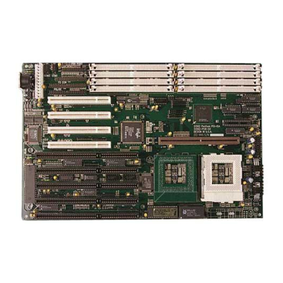
Page 8: S1562 On Board Resource Settings
3. On Board Resource Setting PS/2 Keyboard Figure 3.1 S1562 Board Layout Mouse Header Con7 pin 1 pin 1 KB CTR PWR CON. 5V Com2 J 2 8 J 2 9 pin 1 Com1 J 3 0 J 3 2 J 3 3 J 3 4 J 3 5... -
Page 9: Quick Reference For Jumpers
3.2 Jumper Settings CPU Speed: CPU Speed 1-2, 3-4 Off 75 MHz 90 MHz 100 MHz 120 MHz Cyrix P150+ 133 MHz Cyrix P166+ 150 MHz 166 MHz 200 MHz 1-2, 3-4 100MHz Cyrix P120+ Memory Voltage: 5 volts is the default.Some EDO memory uses 3.3volts. Damage to system can result if these are set incorrectly! Volts Default 5V... - Page 10 I/O Selection: J14 & J15 For COM 1 and 2 Default For InfraRed Speaker Connector: J23 Pinout Assignments Speaker out Ground Ground + 5V Keylock Connector: J22 Pinout Assignments Pins 1 to 3 for power LED. Led Output No Connect Ground Pins 4 and 5 for Keylock Keylock...
- Page 11 Reset Connector: J27 Pinout Assignment Power Good Ground Turbo LED Connector: J25 Pinout Assignment Cathode Anode Flash EEPROM: J47 & J48 These jumpers should be left at the factory default. InfraRed Interface: Con7 and Con9 Pinout Assignment Signal In Signal Out PS/2 Pinout: Data Keyboard...
-
Page 12: Cmos Rtc
Voltage Regulator The Default setting will work with most Pentiums CPU's. The 6x86 will have a marking on it that will identify the voltage that it requires. "016" marking on Cyrix chip uses a 3.3V setting. "028" marking on Cyrix chip uses a 3.48V setting. Default 3.3V 3.48V 3.6V... -
Page 13: Reset Connector
3.7 Hardware Reset Switch Connector Installation The RESET switch on your cases' display panel provides users with the HARDWARE RESET function which is the same as power on/off. The system will do a cold start after the RESET switch is pushed by the user. The RESET switch is a 2 pin connector and should be installed on jumper J27. -
Page 14: Dram Installation
3.10 DRAM Installation The S1562 uses a 64-bit data path from memory to CPU and can accommodate up to 512 MB of RAM. The mainboard supports standard, EDO (Extended Data Out) and ECC(Error Correcting Code) 72 pin SIMMS . All installed memory will be automatically detected so there is no need to set jumpers. - Page 15 Total Memory In Bank Bank0 Bank1 Bank2 Bank3 0&1 0,1&2 Total 4MB*2 (1MB*2) (1MB*2) (1MB*2) 10MB 12MB 14MB 4MB*2 (2MB*2) (2MB*2) (2MB*2) 12MB 16MB 20MB 4MB*2 (4MB*2) (4MB*2) (4MB*2) 16MB 24MB 32MB 4MB*2 (8MB*2) (8MB*2) (8MB*2) 24MB 40MB 56MB 4MB*2 (16MB*2) (16MB*2) (16MB*2) 40MB 72MB...
- Page 16 Total Memory In Bank Bank0 Bank1 Bank2 Bank3 0&1 0,1&2 Total 64MB*2 (1MB*2) (1MB*2) (1MB*2) 128MB 130MB 132MB 134MB 64MB*2 (2MB*2) (2MB*2) (2MB*2) 128MB 132MB 136MB 140MB 64MB*2 (4MB*2) (4MB*2) (4MB*2) 128MB 136MB 144MB 152MB 64MB*2 (8MB*2) (8MB*2) (8MB*2) 128MB 144MB 160MB 176MB 64MB*2 (16MB*2) (16MB*2) (16MB*2) 128MB 160MB 192MB 224MB 64MB*2...
-
Page 17: Cpu Installation
3.11 CPU Installation Many types of Pentiums (75 thru 200 MHz) and Cyrix CPUs can be used on the S1562. Please refer to the previous pages for the correct CPU jumper settings for your board. w The CPU is a sensitive electronic component and it can be easily damaged by static electricity. -
Page 18: Upgrading Cache Memory
3.12 Upgrading Cache Memory The S1562 supports synchronous pipeline burst SRAM. The synchronous pipeline burst cache uses a "COAST Module" that is plugged into the "COAST " socket connector which is located between the CPU and the SIMM sockets. wThe BIOS will auto detect the cache size so a you don't need to change any jumpers. -
Page 19: Understanding The Different Clock Speeds
3.13 Understanding The Different Clock Speeds The following chart shows the different CPU, mainboard and PCI fre- quencies. As you may have noticed, all the Intel Pentium CPUs use an internal clock multiplier(x3, x2.5, x2 or x1.5 Motherboard speed). All Cyrix 6x86 can only use a x2 clock mulitipplier. -
Page 20: Peripheral Device Installation
3.14 Peripheral Device Installation After all the jumpers on the mainboard have been set, then it can be mounted into the case. Then proceed to instalL the display card and any other peripheral devices. If a PCI-Bus interface card is to be installed in the system, any one of the four PCI-Bus slots can support either a Master or a Slave device. -
Page 21: Connecting The Power Supply
3.15 Connecting the Power Supply The system power supply connectors on the mainboard is for a 5 volt power supply. Incorrect installation of the power supply could result in serious damage to the system board and connected peripherals. Pin 1 Good Power Signal 5 volt +12V... - Page 22 Align the plastic guide pins on the lead cables to their receptacles on the mainboard. You may need to hold the lead at an angle to line it up.Once you have the guide pins aligned, press the lead connector so that the plastic clips on the lead snap into place and secure the lead to the connec- tor.
-
Page 23: Bios Configuration
4. BIOS Configuration Award's BIOS has a built in setup program that allows the user to modify the basic system configuration. This type of information is stored in the battery-backed CMOS SRAM. Entering incorrect information or for- getting your password can lock you out of your system.(refer to 3.15 for resetting of CMOS) 4.1. -
Page 24: Control Keys
4.2. Control Keys PgUp key Increases the numeric value or make changes PgDn key Decreases the numeric value or make changes F1 key General help, only for Status Page Setup menu and Option Page Setup Menu F2 key Change color from a total of 16 colors F3 key Calendar, only for Status Page Setup Menu F4 key... -
Page 25: Getting Help
4.3. Getting Help 4.3.1. Main Menu The on-line description of the highlighted setup function is displayed at the bottom of the screen. 4.3.2. Setup Page menu/Option Page Setup Menu Press F1 to pop up a small help window that describes the appropriate keys to use and the possible selections for the highlighted items. - Page 26 w w Standard CMOS setup This setup page includes all the items in a standard compatible BIOS. w w BIOS features setup This setup page includes all of the enhanced features of Award's BIOS. w w Chipset features setup This setup page includes all the items of the 430HX chipset features. w Power Management setup Change, set, or disable system power management options w w PCI slot configuration...
-
Page 27: Standard Cmos Setup Menu
4.5. Standard CMOS Setup Menu The items in Standard CMOS Setup Menu (Figure 4.5) are divided into 9 categories. Each category includes one or more setup items. Use the arrows to highlight the item and use the <PgUp> or <PgDn> keys to select the value you want for each item. - Page 28 w w Primary/Secondary Drive type This category identifies the types of hard disk drives that have been in- stalled in the computer. There are 46 predefined types and a user definable type. Press PgUp or PgDn to select a numbered hard disk type or type a number and press <Enter>.
- Page 29 w w Video This category detects the type of graphics adapter used for the primary display system. It must match your video display card and monitor. Al- though secondary monitors are supported, you do not have to select that type in setup. EGA/VGA Enhanced Graphics Adapter/Video Graphics Array.
-
Page 30: Bios Features Setup
Expanded Memory Expanded Memory (EMS) defines a 64 K page frame in the area between 640K and 1Mb containing four 16K pages that are windows into the EMS memory. Programs issue requests to the EMS manager to switch the page to any part of EMS memory. - Page 31 w w Virus warning This category flashes on screen. During and after the system boot up, any attempt to write to the boot sector or the partition table of the hard disk drive will halt the system and the following error message will appear.
- Page 32 w w Boot Up Floppy Seek During POST, the BIOS will determine if the floppy disk drive installed is 40 or 80 tracks. 360K type is 40 tracks while 720K, 1.2M and 1.44M are all 80 tracks. Default value is Enabled Enabled BIOS searches for floppy disk drive to determined if it is 40 or 80 tracks.
-
Page 33: Chipset Features Setup
w w Security Option This category allows you to limit access to the system setup, or just setup. Default value is Setup System The system will not boot and access to Setup will be denied if the correct password is not entered at the prompt Setup The system will boot, but access to setup will be denied if the password is not entered at the prompt... - Page 34 w w Chipset Features The DRAM timings can be altered from the default to optimize system performance. Be aware though that these settings are sensitive to the type and speed of DRAMs being used and can cause lockups or data lost if set incorrectly.
- Page 35 w w Speculative Leadoff The 430HX chipset is capable of allowing a DRAM read request to be generated slightly before the address has been fully decoded. This can reduce all read latencies. More simply, the CPU will issue a read request and included with this request is the place(address) in memory where the desired data is to be found.
- Page 36 w w Memory Hole at 15M-16M Some ISA cards may not function correctly when more than 16MB of RAM is installed. If this is the case, then enable this option. Most ISA card should work fine with this option disabled. The default is disabled.
- Page 37 w w Peer Concurrency When enabled, multiple PCI devices can be active at any one time. When disabled, only one PCI device can have access to the PCI bus. at any one time. The default is Enabled. w w Chipset Special Features When disabled, the chipset behaves as if it were the earlier 430FX chipset.
-
Page 38: Power Management Setup
4.7.1 Power Management Setup ROM ISA BIOS POWER MANAGEMENT SETUP AWARD SOFTWARE, INC Power Management :Disabled IRQ3 (Com2) :Off PM Control By APM IRQ4 (Com1) :Off Video Off Method :Blank Screen IRQ5 (LPT2) :Off IRQ6 (Floppy Disk) :Off Doze Mode :Disabled IRQ7 (LPT1) :Off... - Page 39 w w Doze Mode Defines the continous idle time before the system enters Doze mode. w w Standby Mode Defines the continous idle time before the system enters Standby mode. w w Power Down Activities Defines the the activities that can cause the PM timers to reload. (Break- ing out of PM Mode) S1562-001-01...
-
Page 40: Pci Slot Configuration
4.8 PCI Slot Configuration ROM ISA BIOS PCI SLOT CONFIGURATION AWARD SOFTWARE, INC. PnP BIOS Auto-Config:Enabled Slot1 Using INT# : AUTO Slot2 Using INT#: AUTO Slot3 Using INT#: AUTO Slot4 Using INT#: AUTO PCI IRQ Activated By: Level PCI IDE IRQ Map To: Auto Primary IDE INT#: Secondary IDE INT#: ESC: Quit... - Page 41 w w PnP BIOS Auto-Config This option lets you enable or disable auto configuration for the Plug and Play BIOS.This should be enabled for PnP operating systems. The default is Enabled. w1st Available IRQ# w w 2nd Available IRQ# w w 3rd Available IRQ# w w 4th Available IRQ# Select four available IRQs assignments to PCI slots INT w w PCI IRQ Activated By:...
-
Page 42: Load Setup Defaults
4.9. LOAD SETUP DEFAULTS ROM ISA BIOS CMOS SETUP UTILITY AWARD SOFTWARE INC. STANDARD CMOS SETUP PASSWORD SETTING BIOS FEATURES SETUP IDE HDD AUTO DETECTION CHIPSET FEATURES SETUP DAVE & EXIT SETUP Load Setup Defaults (Y/N)? N PCI SLOT configuration EXIT WITH OUT SAVING LOAD SETUP DEFAULTS ESC : Save &... - Page 43 ROM ISA BIOS CMOS SETUP UTILITY AWARD SOFTWARE, INC. STANDARD CMOS SETUP PASSWORD SETTING BIOS FEATURES SETUP IDE HDD AUTO DETECTION CHIPSET FEATURES SETUP DAVE & EXIT SETUP Enter Password PCI SLOT CONFIGURATION EXIT WITH OUT SAVING LOAD SETUP DEFAULTS ESC : Save &...
-
Page 44: Ide Hdd Auto Detection
4.11. IDE HDD AUTO DETECTION ROM ISA BIOS CMOS SETUP UTILITY AWARD SOFTWARE, INC. CYLS. HEAD PRECOMP LANZONE SECTORS Drive C: (202 Mb) 65535 Do you want to accept this as drive C (Y/N)? Esc:Skip Type "Y" to accept the H.D.D parameter reported by BIOS. Type "N" to keep the old H.D.D parameter info. -
Page 45: Keyboard Setting Functions
Type "Y" and you will quit the Setup Utility and save the user setup values to RTC CMOS SRAM. Type "N" to return to Setup Utility. 4.13 KEYBOARD SETTING FUNCTION After booting the O.S., there are some special functions used by the key- board as follows: "CTRL_ALT_DEL"... -
Page 46: Ami Winbios
5.0 AMI WINBIOS The AMI WINBIOS is based on a Graphical User Interface that enables the user to access all of the BIOS setup options with either a mouse or keyboard. You can enter the BIOS setup by pressing the "DEL" key during the memory test/count. -
Page 47: Advanced Setup
w w Primary/Secondary Master w w Primary/Secondary Slave Select one of these hard disk drive icons to configure the drive named in the option. WINBIOS supports up to four IDE hard disk drives: the primary master, primary slave, secondary master and secondary slave. If the hard disk drive is an IDE drive, select DETECT PRIMARY or DETECT SLAVE from the Utility Setup Option Section of the WINBIOS Setup Main Menu to have WINBIOS automatically detect the IDE drive parameters and re-... - Page 48 w w BootUp Num-Lock This option gives the user the option to turn on or off the num-lock on boot-up. The default is On. w w Floppy Drive Swap When enabled, the system allows the floppy drives to swap drive letters with each other.
- Page 49 w w System BIOS Cacheable If this option is enabled, the F000 segment of the BIOS shadow will be cached. The default is enabled. w w Adaptor ROM Shadow C000 to DC00 The adaptor ROMs present on the system may either execute out of ROM(disabled), RAM(Shadow), or execute out of RAM and be cached(Cache).
-
Page 50: Advanced Chipset
5.3 Advanced Chipset w w Global 430HX Enable This option provides a method to enable or disable all of the additional features provided by the 430HX chipset(enhancements to 430FX). w w Shutdown to Port 92 When disabled, the 430HX forwards a Shutdown special cycle from the host bus to the PCI bus. - Page 51 Refresh Rate Allows the refresh rate to be set according to the memory bus clock (50mhz, 60mhz or 66mhz). The default depends on CPU speed. Turbo Read LeadOff A feature to enable the skipping of the first input register in the DRAM data pipeline.
- Page 52 Memory Address Drive Strength This setup option allows the selection of memory address output buffer drive affecting the MA(memory address) and MWE#(memory write enale)pins. The default is 8ma/8ma. NA Disable (NAD) For External Cache When enabled the NA#(next address) pin is never asserted, otherwise the assertion is dependent upon the cache type and size.
- Page 53 SingleBit Correctable Error This option if enabled will assert SERR# upon the detection of a single bit error (SBE). The default is disabled. MultiBit Uncorrectable Error This option if enabled will assert SERR# upon the detection of a multi bit error (MBE) or parity error. The default is disabled. Bad Parity On Uncorrectable Error The TXC forces bad parity on PCI read data starting from the time an uncorrectable DRAM error is detected,until the end of the current...
-
Page 54: Power Management
5.4 Power Management w w Advanced Power Management This option enables or disables power management. The default is disabled. w w Standby to Suspend Timeout Value This option indicates the time before standby and suspend power saving modes will occur. The options are from disabled thru 255 minutes. The default is disabled. -
Page 55: Peripheral
5.5 Peripheral w w Programming Mode When set to manual, you can customize all the settings below. When set to auto, they system will automatically configure all the ports. The default is Manual. w w OnBoard FDC This option lets you enable or disable the onboard floppy disk controller. The default is enabled. -
Page 56: Utility
5.6 Utility Detect Master/Detect Slave These options, when invoked will enable the CMOS to query the IDE drive firmware for its cylinder, head and sector parameters. Color Set This option lets you select the color scheme of the WinBIOS setup LCD, Army, Pastel and Sky. -
Page 57: Flash Writer Utility
6.0 Flash Writer Utility You can upgrade the BIOS of your mainboard by using a "Flash Memory Writer"(FMW) utility. This utility can be downloaded from the factory's BBS(Consult your system vendor for the phone #). The system BIOS is stored on a 'flash' EPROM chip on the mainboard which can be erased and reprogrammed by the FMW. - Page 58 To reprogram the System BIOS, you must first do the following: 1. Check jumpers J47 and J48 The S1562 uses a 5V Flash EPROM so these three jumpers should be left in the default postion on pins 1 and 2. These jumpers should never be moved.
-
Page 59: The Flash Memory Writer Utility Screen
Once you have satisfied the two requirements mentioned above, you can run FMW. You can copy the contents of the “Flash” directory to your hard drive, or you can run the utility from a backup of the support floppy disk. Make sure the new BIOS file is in the same directory as the FMW utility. -
Page 60: At Technical Information
7.0 AT TECHNICAL INFORMATION 7.1 I/O BUS CONNECTOR PIN OUT 7.1.1 ISA SLOT PIN OUT -I/O CH CHK -MEMC16 SBHE SD07 -I/OCS16 LA23 RESET SD06 IRQ10 LA22 SD05 IRQ11 LA21 IRQ9 SD04 IRQ12 LA20 SD03 IRQ15 LA19 DRQ2 SD02 IRQ14 LA18 -12V SD01... -
Page 61: Pci-Bus Slot Pin Out
7.1.2 PCI-BUS SLOT PIN OUT -12V +12V INT#A INTB# INT#C INTD# PST#1 PST#2 RST# GNT# REQ# AD_31 AD_30 AD_29 AD_28 AD_27 AD_26 AD_25 AD_24 CBE#3 IDSEL AD_23 AD_22 AD_21 AD_20 AD_19 AD_18 AD_17 AD_16 CEB#2 FRAME# IRDY# STOP# DEVSEL# SDONE LOCK# SBO# PERR#... -
Page 62: Timer & Dma Channel Map
7.2. TIMER & DMA CHANNEL MAP TIMER MAP: TIMER Channel-0 system timer interrupt TIMER Channel-1 DRAM REFRESH request TIMER Channel-2 SPEAKER tone generator DMA CHANNELS: DMA Channel-0 Available DMA Channel-1 Available DMA Channel-2 FLOPPY DISK adapter DMA Channel-3 Available DMA Channel-4 Cascade for DMA controller 1 DMA Channel-5 Available DMA Channel-6 Available DMA Channel-7 Available... -
Page 63: Rtc & Cmos Ram Map
7.4 RTC & CMOS RAM MAP RTC & CMOS: Seconds Seconds alarm Minutes Minutes alarm Hours Hours alarm Days of the week Days of the month Month Year Status register A Status register B Status register C Status register D Diagnostic status byte Shutdown byte Floppy DISK drive type byte... -
Page 64: Appendix A. Post Codes
Appendix A: Post Codes ISA POST codes are typically output to port address 80h ( Award BIOS) POST Name OEM specific-Cache control Turn off Processor Status (1 FLAGS) verification. Chipset cache Processor Test 1 Test the following processor status flags; carry, zero, sign, overflow. - Page 65 Test DMA memory Test DMA controller controller 1 Test DMA Page Test DMA page Registers registers 12-13 reserved Test timer Test 8254 timer 0 counter 2 counter 2 Test 8259-1 Verify 8259 channel 1 masked interrupts Mask Test 8259-2 Verify 8259 channel 2 masked interrupts Mask Test Stuck 8259 Turn off interrupt then verify nointerrupt mask register is on...
- Page 66 Manufacturing Reboot if manufacturing POST loop pin is set. Otherwise POST loop or display any messages(i.e. non fatal errors that were detected display messages during POST) and enter setup Security check Ask password security (optional) Write CMOS Write all CMOS values back to RAM and clear screen PRE-boot enable Enable parity checker, enable NMI and enable cache before boot...
Need help?
Do you have a question about the TOMCAT I II and is the answer not in the manual?
Questions and answers