Advertisement
DESCRIPTION
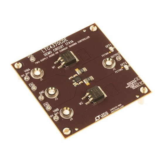
Demonstration circuit DC1741A features the LTC4370, a
two supply diode-OR current sharing controller in a typical
2.9V to 18V, 16A sharing application.
The maximum MOSFET voltage drop V
set with an external resistor, up to 600mV. A fast gate
turn-on reduces the load voltage droop during supply
switchover. If the input supply fails or is shorted, a fast
turn-off minimizes the transient reverse current.
Disabling the load sharing function turns the LTC4370
into a dual ideal diode controller.
Two enable input pins, EN1 and EN2, allow enabling and
disabling each rail's MOSFET individually while the MOS-
FETs' inherent diodes create diode-OR connection when
the MOSFETs are disabled. The LTC4370 provides a rich
PERFORMANCE SUMMARY
SYMBOL
PARAMETER
V
V
and V
IN
IN1
V
V
External Supply Operating Range
CC(EXT)
CC
V
V
Regulated Voltage
CC(REG)
CC
V
Error Amplifier Input Offset
EA(OS)
g
Error Amplifier Gain
m(EA)
V
Forward Regulation Voltage (V
FR
ΔV
MOSFET Gate Drive (GATE-V
GATE
I
GATE1, GATE2 Fast Pull-Up Current
GATE
GATE1, GATE2 Fast Down-Up Current
GATE1, GATE2 Off Pull-Down Current
EN1, EN2 Threshold Voltage
V
EN(TH)
ΔV
MOSFET On-Detect Threshold (GATE-V
GATE(ON)
I
Maximum Continuous Load Current
OUT
Arrow.com.
Downloaded from
= V
FR
Input Voltage Operating Range
IN2
– V
)
IN
OUT
)
IN
)
IN
DEMO MANUAL DC1741A
Two-Supply Diode-OR
Current Balancing Controller
set of features to support shared current diode-ORed ap-
plications including:
• Load Sharing Between Two Supplies
– OUT is
IN
• Elimination of the Need for Active Control of Input
Supplies
• Elimination of "Share Bus"
• Reverse Current Blocking
• Elimination of Shoot-Through Current During Start-Up
or Faults
Design files for this circuit board are available at
http://www.linear.com/demo
L, LT, LTC, LTM, Linear Technology and the Linear logo are registered trademarks of Linear
Technology Corporation. All other trademarks are the property of their respective owners.
Specifications are at T
= 25°C
A
CONDITIONS
With External V
Supply
CC
V
, V
≤ V
IN1
IN2
CC
V
=1.2V, V
= 5V
IN
CC
V
=12V
IN
V
= 0.2V; I = 0, –1μA; Highest V
FWD
V
= 0.2V; I = 0, –1μA; Highest V
FWD
V
= 0.4V, ΔV
= 0V, CPO = 17V
FWD
GATE
V
= –2V, ΔV
= 5V,
FWD
GATE
Corresponding EN =1V, ΔV
= 2.5V
GATE
EN Falling
FETON Transitions High
Sharing active, limited by SUM85N03 FET Dissipation
MIN
TYP
2.9
0
2.9
4.5
5
0
150
2
12
2
25
= 12V
10
12
IN
= 2.9V
4.5
7
IN
–0.9
–1.4
0.9
1.4
65
110
580
600
0.28
0.7
LTC4370
MAX
UNITS
18
V
V
CC
6.0
V
5.5
V
±2
mV
μS
25
mV
50
mV
14
V
9
V
–1.9
A
1.9
A
160
μA
620
mV
1.1
V
16.6
A
dc1741af
1
Advertisement
Table of Contents

Related Manuals for Linear Technology LTC4370


Summary of Contents for Linear Technology LTC4370
- Page 1 FETs’ inherent diodes create diode-OR connection when L, LT, LTC, LTM, Linear Technology and the Linear logo are registered trademarks of Linear the MOSFETs are disabled. The LTC4370 provides a rich Technology Corporation. All other trademarks are the property of their respective owners.
-
Page 2: Operating Principles
DEMO MANUAL DC1741A OPERATING PRINCIPLES The LTC4370 controls N-channel MOSFETs, M1 and Two LEDs, OFF1 and OFF2, indicate the MOSFETs’ status. M2, to share the load between two input rails.The error Each LED lights up, when the gate voltage is less than amplifier compares OUT1 and OUT2, and controls servo 0.7V above V... -
Page 3: Quick Start Procedure
Demonstration circuit DC1741A is easy to set up to evalu- 2. Reduce the load current to a total of 7.5A. Adjust the ate the performance of the LTC4370. Refer to Figure 1 two 5V supplies’ outputs to a voltage difference of 373 for proper measurement equipment setup for load share mV which equals the maximum ΔV... -
Page 4: Parts List
Res., Chip 30.1k, 0.1W 1%, 0805 Vishay, CRCW080530K1FKEA R4, R6 Res., Chip 10k, 0.1W, 5%, 0805 Vishay, CRCW080510K0JNEA R5, R7 Res., 0805 I.C., Diode-OR Load Share Cont., DFN16DE-4 × 3 Linear Technology Corp., LTC4370CDE dc1741af Arrow.com. Arrow.com. Arrow.com. Arrow.com. Downloaded from Downloaded from... -
Page 5: Schematic Diagram
Information furnished by Linear Technology Corporation is believed to be accurate and reliable. However, no responsibility is assumed for its use. Linear Technology Corporation makes no representa- tion that the interconnection of its circuits as described herein will not infringe on existing patent rights. - Page 6 Linear Technology Corporation (LTC) provides the enclosed product(s) under the following AS IS conditions: This demonstration board (DEMO BOARD) kit being sold or provided by Linear Technology is intended for use for ENGINEERING DEVELOPMENT OR EVALUATION PURPOSES ONLY and is not provided by LTC for commercial use. As such, the DEMO BOARD herein may not be complete in terms of required design-, marketing-, and/or manufacturing-related protective considerations, including but not limited to product safety measures typically found in finished commercial goods.
Need help?
Do you have a question about the LTC4370 and is the answer not in the manual?
Questions and answers