Advertisement
Quick Links
Description
Demonstration circuit DC1555C is intended to demon-
strate the performance of the LTC4365 and LTC4365-1
Undervoltage, Overvoltage and Reverse Supply Protection
Controllers.
The
LTC
4365/LTC4365-1
®
ages that may be too high, too low or negative. It operates
by controlling the gates of two back-to-back connected
MOSFETs to keep the output in a safe range. The OV and
UV protection levels are adjusted by resistive dividers at
the OV and UV pins. Asserting the SHDN pin disables the
MOSFETs and places the controller in a low-current shut-
down state. The FAULT pin is asserted when the Controller
is in shutdown mode or when the input voltage is outside
of the UV or OV level.
The LTC4365 and LTC4365-1 can withstand DC voltages
between –40V and +60V and have a valid operating range
of 2.5V to 34V.
performance summary
SYMBOL
PARAMETER
VIN
Board Input Voltage Range
V
Input Supply Undervoltage Lockout
IN(UVLO)
I
Input Supply Current
VIN
I
Reverse Input Supply Current
VIN(R)
ΔV
External N-Channel Gate Drive (GATE – VOUT)
GATE
I
External N-Channel Gate Pull-Up current
GATE(UP)
I
External N-Channel Fast Gate Pull-Down Current
GATE(FAST)
I
External N-Channel Gentle Gate Pull-Down Current Gentle Shutdown, GATE = 20V, VIN = VOUT = 12V
GATE(SLOW)
V
UV Input Threshold Voltage
UV
V
OV Input Threshold Voltage
OV
t
External N-Channel Fast Gate Turn-Off Delay
GATE(FAST)
t
OV, UV Fault Propagation Delay
FAULT
V
SHDN Input Threshold
SHDN
Overvoltage, Undervoltage and
Reverse Supply Protection Controller
protect circuits from input volt-
(T
= 25°C)
A
CONDITIONS
VIN Rising
SHDN = 0V
SHDN = 2.5V
VIN = –40V, V
VIN = VOUT = 5V, I
VIN = VOUT = 12V to 34V, I
GATE = VIN = VOUT = 12V
Fast Shutdown, GATE = 20V, VIN = VOUT = 12V
UV Falling → ΔV
OV Rising → ΔV
C
Overdrive = 50mV, VIN = VOUT = 12V
SHDN Falling to ΔV
DEMO MANUAL DC1555C
LTC4365/LTC4365-1:
Regarding the supply protection parameters, the LTC4365
and LTC4365-1 are identical. The only differences are
in the gate fault recovery delay time and the delay from
turn-off to low-power operation. These delays are 36ms
(typ, both) for the LTC4365, while they are 1ms and 0.7ms
respectively for the LTC4365-1.
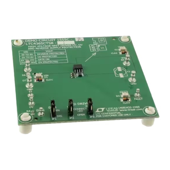
The DC1555C includes the controller, two back-to-back
connected power MOSFETs, three jumpers and three
LEDs to indicate the input and output voltages and the
FAULT pin signal.
Design files for this circuit board are available at
http://www.linear.com/demo/DC1555C
L, LT, LTC, LTM, Linear Technology and the Linear logo are registered trademarks of Linear
Technology Corporation. All other trademarks are the property of their respective owners.
= 0V
OUT
= –1µA
GATE
= –1µA
GATE
= 0V
GATE
= 0V
GATE
= 2.2nF, UV or OV Fault
GATE
= 0V
GATE
MIN
TYP
MAX
UNITS
–30
30
1.8
2.2
2.4
10
50
µA
25
150
µA
–1.2
–1.8
mA
3
3.6
4.2
7.4
8.4
9.8
–12
–20
–30
µA
31
50
72
mA
50
90
150
µA
492.5
500
507.5
mV
492.5
500
507.5
mV
2
4
µs
1
2
µs
0.4
0.75
1.2
dc1555cfd
1
V
V
V
V
V
Advertisement

Subscribe to Our Youtube Channel
Related Manuals for Linear Technology LTC4365


Summary of Contents for Linear Technology LTC4365
- Page 1 L, LT, LTC, LTM, Linear Technology and the Linear logo are registered trademarks of Linear of the UV or OV level. Technology Corporation. All other trademarks are the property of their respective owners.
-
Page 2: Operating Principles
The LTC4365 provides During normal operation, a high voltage charge pump accurate overvoltage and undervoltage comparators to enhances the gate of external N-channel power MOSFETs. -
Page 3: Quick Start Procedure
The Si4214 FET limits overvoltage and reverse FAULT LED, green VOUT LED, and VOUT according to voltage to 30V and –30V, respectively. Refer to the LTC4365 Table 1 within the various voltage ranges. data sheet for applications optimized for other voltages. - Page 4 DEMO MANUAL DC1555C Quick start proceDure Figure 1a. Undervoltage/Overvoltage Measurement Figure 1b. Reverse Voltage Measurement dc1555cfd...
-
Page 5: Schematic Diagram
Information furnished by Linear Technology Corporation is believed to be accurate and reliable. However, no responsibility is assumed for its use. Linear Technology Corporation makes no representa- tion that the interconnection of its circuits as described herein will not infringe on existing patent rights. - Page 6 Linear Technology Corporation (LTC) provides the enclosed product(s) under the following AS IS conditions: This demonstration board (DEMO BOARD) kit being sold or provided by Linear Technology is intended for use for ENGINEERING DEVELOPMENT OR EVALUATION PURPOSES ONLY and is not provided by LTC for commercial use. As such, the DEMO BOARD herein may not be complete in terms of required design-, marketing-, and/or manufacturing-related protective considerations, including but not limited to product safety measures typically found in finished commercial goods.
- Page 7 Mouser Electronics Authorized Distributor Click to View Pricing, Inventory, Delivery & Lifecycle Information: Analog Devices Inc. DC1555C-B DC1555C-A...
Need help?
Do you have a question about the LTC4365 and is the answer not in the manual?
Questions and answers