Advertisement
www.ti.com
EVM User's Guide: LM25137F-Q1-EVM5D3
LM25137-Q1 Evaluation Module
Description
The LM25137F-Q1-EVM5D3 evaluation module
(EVM) is designed to showcase the LM(2)5137-Q1
and LM(2)5137 dual, synchronous buck controller,
which is intended for
functional safety
to ASIL D or SIL 3. The EVM operates over a wide
input voltage range of 6.5V to 36V to deliver 5V and
3.3V regulated outputs with better than 1% setpoint
accuracy at load currents up to 20A per output.
Get Started
1. Order the LM25137F-Q1-EVM5D3.
2. Refer to the
LM5137-Q1
product folders.
3. Review the Altium
PCB layout
4. Use the LM(2)5137-Q1
assist with component selection in your design.
Features
•
Maximum inout voltage of 36V
– V
UVLO thresholds set at 6.5V and 4.5V
IN
•
Tightly regulated output voltages of 5V and 3.3V,
each rated at 20A with 1mV load, line regulation
•
High efficiency – 96% at 10A, 94% at 20A
– VCC bias power derived from the 5V output
•
Switching frequency of 440kHz synchronizable
±20% with an external clock signal
SNVU907A – JULY 2024 – REVISED AUGUST 2024
Submit Document Feedback
applications up
and
LM25137-Q1
source files.
quickstart calculator
to
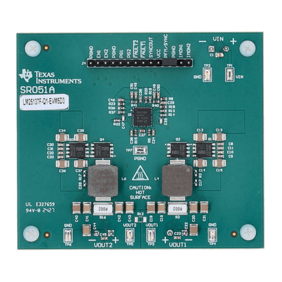
LM25137-Q1 EVM, 84mm × 74mm
Copyright © 2024 Texas Instruments Incorporated
•
Input π-stage EMI filter meets CISPR 25
– Spread spectrum (DRSS) option for lower EMI
– Electrolytic capacitor for parallel damping
•
Peak current-mode control architecture provides
fast line and load transient response
– Integrated slope compensation
– Forced PWM (FPWM) or pulsed frequency
modulation (PFM) operation
•
Integrated power MOSFET gate drivers
– 3A/2A sink/source gate drive current capability
– Adaptive dead-time control reduces power
dissipation and MOSFET temperature rise
•
Integrated protection features for robust design
– Overcurrent protection (OCP) with shunt or
inductor DCR current sensing
– Monotonic prebias output voltage startup
– User-adjustable soft-start time set to 4.5ms
– PG and FAULT outputs for each channel
– Dual current monitor outputs (IMON1, IMON2)
•
Fully assembled, tested and proven PCB layout
with 3.3" × 2.9" (84mm × 74mm) total footprint
Applications
•
High-current
automotive electronic systems
2-, 3- and 4-phase implementations
•
Dual outputs for
ADAS
•
Infotainment systems
•
Automotive HEV/EV powertrain systems
Description
using
and
body
electronics
and
instrument clusters
LM25137-Q1 Evaluation Module
1
Advertisement
Table of Contents

Subscribe to Our Youtube Channel
Related Manuals for Texas Instruments LM25137-Q1


Summary of Contents for Texas Instruments LM25137-Q1
- Page 1 Switching frequency of 440kHz synchronizable • Automotive HEV/EV powertrain systems ±20% with an external clock signal LM25137-Q1 EVM, 84mm × 74mm SNVU907A – JULY 2024 – REVISED AUGUST 2024 LM25137-Q1 Evaluation Module Submit Document Feedback Copyright © 2024 Texas Instruments Incorporated...
-
Page 2: Kit Contents
Independent current monitor (IMON), power good (PG) and FAULT indicator outputs on each channel 1.2 Kit Contents • A complete filter board (EVM) rated at 20A on each output, including the LM25137-Q1 buck controller IC • EVM Disclaimer Read Me LM25137-Q1 Evaluation Module SNVU907A –... -
Page 3: Specifications
The default output voltages of this EVM are 5V and 3.3V. Efficiency and other performance metrics can change based on the operating input voltage, load currents, externally-connected output capacitors and other parameters. SNVU907A – JULY 2024 – REVISED AUGUST 2024 LM25137-Q1 Evaluation Module Submit Document Feedback Copyright © 2024 Texas Instruments Incorporated... - Page 4 Evaluation Module Overview www.ti.com 1.3.1 Application Circuit Diagrams Figure 1-1 shows an LM25137-Q1 synchronous buck regulator (not including the EMI filter stage). Furthermore, as detailed in Figure 1-2, we implement a two-phase, single-output regulator by tying the outputs together, connecting COMP1 to COMP2, shorting FB2 to AGND, and setting the CNFG resistor to 41.2kΩ.
-
Page 5: Device Information
With the LM5137-Q1 and LM25137-Q1 now available to aid in functional safety system design up to ASIL D, the controller family enables DC/DC designs with high density, low EMI and increased system reliability. All controllers are rated for a maximum operating junction temperature of 150°C and have AEC-Q100 grade 1... - Page 6 Power Good outputs FAULT1, FAULT2 FAULT outputs SYNCOUT Synchronization output Bias rail connection PFM/SYNCIN Synchronization input IMON1, IMON2 Current monitor outputs LM25137-Q1 Evaluation Module SNVU907A – JULY 2024 – REVISED AUGUST 2024 Submit Document Feedback Copyright © 2024 Texas Instruments Incorporated...
- Page 7 OUT2 • Decrease the load to 0A. Decrease the input source voltage to 0V. SNVU907A – JULY 2024 – REVISED AUGUST 2024 LM25137-Q1 Evaluation Module Submit Document Feedback Copyright © 2024 Texas Instruments Incorporated...
- Page 8 = 12V = 24V = 36V Output Current (A) Figure 3-3. Ch2 Efficiency, V = 3.3V, FPWM, Channel 1 OFF OUT2 LM25137-Q1 Evaluation Module SNVU907A – JULY 2024 – REVISED AUGUST 2024 Submit Document Feedback Copyright © 2024 Texas Instruments Incorporated...
- Page 9 Figure 3-7. Ch2 (3.3V) Load Transient Response, = 12V, FPWM, 0A to 20A at 2A/µs = 12V, FPWM, 0A to 10A at 2A/µs SNVU907A – JULY 2024 – REVISED AUGUST 2024 LM25137-Q1 Evaluation Module Submit Document Feedback Copyright © 2024 Texas Instruments Incorporated...
- Page 10 Figure 3-11. Shutdown Characteristic, V = 12V, 12V, I = 5A Resistive, R = 20kΩ = 5A Resistive OUT1 OUT2 OUT1 OUT2 LM25137-Q1 Evaluation Module SNVU907A – JULY 2024 – REVISED AUGUST 2024 Submit Document Feedback Copyright © 2024 Texas Instruments Incorporated...
- Page 11 OUT2 3.1.2.4 Switching SW1 5V/DIV SW2 5V/DIV 400ns/DIV Figure 3-13. Switch-node Voltages, V = 12V, I = 10A OUT1 OUT2 SNVU907A – JULY 2024 – REVISED AUGUST 2024 LM25137-Q1 Evaluation Module Submit Document Feedback Copyright © 2024 Texas Instruments Incorporated...
- Page 12 EMI Training Series • Application Note: – Improve High-current DC/DC Regulator EMI Performance for Free With Optimized Power Stage Layout LM25137-Q1 Evaluation Module SNVU907A – JULY 2024 – REVISED AUGUST 2024 Submit Document Feedback Copyright © 2024 Texas Instruments Incorporated...
- Page 13 COMP1 COMP2 PFM/SYNC IMON1 10.0k 7.50k IMON2 68pF 68pF 36.5k 36.5k PGND 3.3nF 3.3nF PGND AGND Figure 4-1. EVM Schematic SNVU907A – JULY 2024 – REVISED AUGUST 2024 LM25137-Q1 Evaluation Module Submit Document Feedback Copyright © 2024 Texas Instruments Incorporated...
- Page 14 EVM is essentially a single-sided design except for certain input filtering and small-signal components located on the bottom side. Figure 4-2. Top Copper (Top View) Figure 4-3. Layer 2 Copper (Top View) LM25137-Q1 Evaluation Module SNVU907A – JULY 2024 – REVISED AUGUST 2024 Submit Document Feedback Copyright © 2024 Texas Instruments Incorporated...
- Page 15 Hardware Design Files Figure 4-4. Layer 3 Copper (Top View) Figure 4-5. Layer 4 Copper (Top View) SNVU907A – JULY 2024 – REVISED AUGUST 2024 LM25137-Q1 Evaluation Module Submit Document Feedback Copyright © 2024 Texas Instruments Incorporated...
- Page 16 Hardware Design Files www.ti.com Figure 4-6. Layer 5 Copper (Top View) Figure 4-7. Bottom Copper (Top View) LM25137-Q1 Evaluation Module SNVU907A – JULY 2024 – REVISED AUGUST 2024 Submit Document Feedback Copyright © 2024 Texas Instruments Incorporated...
- Page 17 Hardware Design Files 4.2.1 Component Drawings Figure 4-8. Top Component Drawing Figure 4-9. Bottom Component Drawing SNVU907A – JULY 2024 – REVISED AUGUST 2024 LM25137-Q1 Evaluation Module Submit Document Feedback Copyright © 2024 Texas Instruments Incorporated...
- Page 18 HO and SW traces together to minimize gate loop parasitic inductance. LM25137-Q1 Evaluation Module SNVU907A – JULY 2024 – REVISED AUGUST 2024 Submit Document Feedback Copyright © 2024 Texas Instruments Incorporated...
- Page 19 Improve High-current DC/DC Regulator Performance for Free with Optimized Power Stage Layout application brief for more detail. Figure 4-12. PCB Stack-Up Diagram With Low L1-L2 Intra-layer Spacing SNVU907A – JULY 2024 – REVISED AUGUST 2024 LM25137-Q1 Evaluation Module Submit Document Feedback Copyright © 2024 Texas Instruments Incorporated...
- Page 20 TP6, TP7 IC, LM5137-Q1, 80V dual synchronous buck controller, VQFN-36 LM5137FDQRHARQ1 PCB1 PCB, FR4, 6 layer, 2oz, 84mm × 74mm – LM25137-Q1 Evaluation Module SNVU907A – JULY 2024 – REVISED AUGUST 2024 Submit Document Feedback Copyright © 2024 Texas Instruments Incorporated...
-
Page 21: Additional Information
PowerPAD ™ is a trademark of Texas Instruments. WEBENCH ® is a registered trademark of Texas Instruments. All trademarks are the property of their respective owners. 6 Device and Documentation Support 6.1 Device Support 6.1.1 Development Support For development support see the following: •... -
Page 22: Revision History
First public release of the EVM user's guide...................... • Updated the hardware image..........................• Updated the application circuit diagrams......................4 • Added Section 4.2.2 ............................LM25137-Q1 Evaluation Module SNVU907A – JULY 2024 – REVISED AUGUST 2024 Submit Document Feedback Copyright © 2024 Texas Instruments Incorporated... - Page 23 STANDARD TERMS FOR EVALUATION MODULES Delivery: TI delivers TI evaluation boards, kits, or modules, including any accompanying demonstration software, components, and/or documentation which may be provided together or separately (collectively, an “EVM” or “EVMs”) to the User (“User”) in accordance with the terms set forth herein.
- Page 24 www.ti.com Regulatory Notices: 3.1 United States 3.1.1 Notice applicable to EVMs not FCC-Approved: FCC NOTICE: This kit is designed to allow product developers to evaluate electronic components, circuitry, or software associated with the kit to determine whether to incorporate such items in a finished product and software developers to write software applications for use with the end product.
- Page 25 www.ti.com Concernant les EVMs avec antennes détachables Conformément à la réglementation d'Industrie Canada, le présent émetteur radio peut fonctionner avec une antenne d'un type et d'un gain maximal (ou inférieur) approuvé pour l'émetteur par Industrie Canada. Dans le but de réduire les risques de brouillage radioélectrique à...
- Page 26 www.ti.com EVM Use Restrictions and Warnings: 4.1 EVMS ARE NOT FOR USE IN FUNCTIONAL SAFETY AND/OR SAFETY CRITICAL EVALUATIONS, INCLUDING BUT NOT LIMITED TO EVALUATIONS OF LIFE SUPPORT APPLICATIONS. 4.2 User must read and apply the user guide and other available documentation provided by TI regarding the EVM prior to handling or using the EVM, including without limitation any warning or restriction notices.
- Page 27 Notwithstanding the foregoing, any judgment may be enforced in any United States or foreign court, and TI may seek injunctive relief in any United States or foreign court. Mailing Address: Texas Instruments, Post Office Box 655303, Dallas, Texas 75265 Copyright © 2023, Texas Instruments Incorporated...
- Page 28 TI products. TI’s provision of these resources does not expand or otherwise alter TI’s applicable warranties or warranty disclaimers for TI products. TI objects to and rejects any additional or different terms you may have proposed. IMPORTANT NOTICE Mailing Address: Texas Instruments, Post Office Box 655303, Dallas, Texas 75265 Copyright © 2024, Texas Instruments Incorporated...
Need help?
Do you have a question about the LM25137-Q1 and is the answer not in the manual?
Questions and answers