Table of Contents
Advertisement
Quick Links
Advertisement
Table of Contents

Related Manuals for National Instruments PXIe-5830


Summary of Contents for National Instruments PXIe-5830
- Page 1 PXIe-5830 Features 2024-04-01...
-
Page 2: Table Of Contents
PXIe-5830 Block Diagram........ - Page 3 PXIe-5830 Features Frequency and Bandwidth Configuration....... . 30 Frequency and Bandwidth Selection....... . 33 Automatic Frequency Offset.
-
Page 4: Pxie-5830
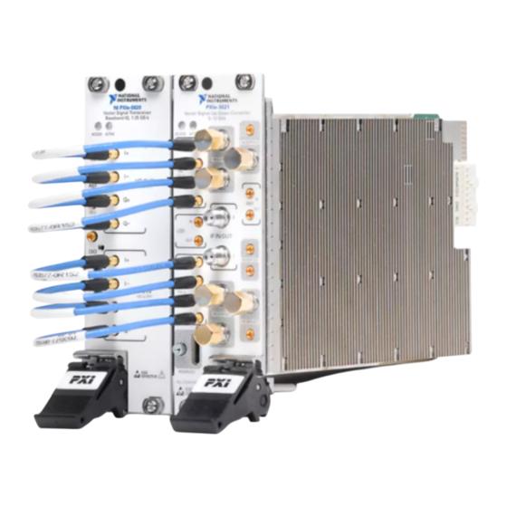
Two 5 GHz to 12 GHz bi-directional IF test ports ■ 1 GHz signal bandwidth ■ Instrument Components The PXIe-5830 is a modular vector signal transceiver instrument consisting of PXI Express hardware. The PXIe-5830 is comprised of the following modules: PXIe-5820 Vector Signal Transceiver ■... -
Page 5: Pxie-5830 Block Diagram
RESERVED Q– RESERVED SENSITIVE ALL COAXIAL PORTS 50 Ω SENSITIVE PXIe-5830 Block Diagram The PXIe-5830 is an IF vector signal transceiver instrument comprised of the PXIe-5820 and PXIe-3621. The following block diagram represents the PXIe-5830 instrument configuration. © National Instruments... - Page 6 PXIe-5830 Features Ref In Ref Out Timing and Sync Engine I DAC PCIe Gen 3 x8 Q DAC IF Out FPGA IF In I ADC Triggers Q ADC PFI 0 Note Some calibration-related routing paths and front panel connectors have been omitted from the illustration of the high-level block diagram for simplicity.
-
Page 7: Local Oscillator
Local Oscillator ■ Local Oscillator The PXIe-5830 contains a local oscillator (LO) for analyzing and generating RF signals. • LO2—Mixed within the PXIe-3621 with the I/Q signals from the PXIe-5820 to analyze or generate an signal between 5 GHz and 12 GHz. You can use this signal to analyze or generate RF signals from the IF bi-directional ports on the PXIe-3621 front panel. - Page 8 PXIe-5830 Features Figure 2. PXIe-5820 Front Panel and LEDs ni.com...
- Page 9 PXIe-5830 Features Table 1. General Connector Descriptions Connector Description Connector Type REF IN Input connector that MMPX (f) allows for the use of an external 10 MHz Reference Clock. REF OUT Output connector that MMPX (f) can export a 10 MHz Reference Clock.
- Page 10 PXIe-5830 Features Connector Description Connector Type Input connector for Q- MMPX (f) signals. Table 3. LED Indicators Indications ACCESS Indicates the basic hardware status of the device. Off—The device is not yet functional or has detected a problem with a PXI Express power rail.
-
Page 11: Pxie-5820 Block Diagram
PXIe-5830 Features Figure 3. PXIe-5820 DIO Connector Pinout Reserved 5.0 V MGT Rx+ 0 MGT Tx+ 0 MGT Rx– 0 MGT Tx– 0 MGT Rx+ 1 MGT Tx+ 1 MGT Rx– 1 MGT Tx– 1 DIO 4 DIO 6 DIO 5... -
Page 12: Pxie-3621
5 GHz to 12 GHz, Vector Signal Up/Down Converter 5 GHz to 12 GHz frequency range ■ Used only within the PXIe-5830 Vector Signal Transceiver instrument as an ■ up and down converter between baseband I/Q and IF signals PXIe-3621 Front Panel and LEDs... - Page 13 PXIe-5830 Features Table 4. I/Q Connector Descriptions Connector Description Connector Type I/Q IN Input connector for I+ MMPX (f) signals. Input connector for I- MMPX (f) signals. Input connector for Q+ MMPX (f) signals. Input connector for Q- MMPX (f) signals.
- Page 14 Reference Clock. Output connector for MMPX (f) the Reference Clock. RESERVED Reserved connectors — are not enabled for use on the PXIe-5830 and should remain capped with 50 Ω terminators to ensure specified instrument performance. Table 6. LED Indicators Indications...
-
Page 15: Instrument Terminology
PXIe-5830 Features Instrument Configurations ■ Instrument Terminology Refer to the following list for definitions of common PXIe-5830 instrument terms used throughout this document. Table 7. Instrument Terminology Definitions Term Definition IF IN/OUT Ports Refers to the IF IN/OUT 0 and IF IN/OUT 1 connectors on the PXIe-3621 front panel for IF signals. -
Page 16: Instrument Configurations
Refers to the NI-RFSA Downconverter Frequency Offset Mode property or NI-RFSG Upconverter Frequency Offset Mode property set to Enabled. The PXIe-5830 contains a direct conversion architecture. Offset mode allows the instrument to operate in low IF mode, which increases the... -
Page 17: Timing Configurations
• 10 MHz PXI Express Backplane Clock—This 10 MHz Reference Clock signal is supplied on the PXI backplane. Configuring Onboard Reference Clock Timing The configuration of the PXIe-5830 exports a 10 MHz signal from the PXIe-3621 to PXIe-5820. Complete the following steps to apply this configuration. -
Page 18: Selecting Available Ports
2. Set the NI-RFSA or NI-RFSG Ref Clock Source property or attribute to RefIn as the Reference Clock source. Configuring PXI 10 MHz Backplane Clock Timing To configure the PXIe-5830 to use the PXI 10 MHz backplane clock, set the NI-RFSA or NI-RFSGRef Clock Source property or attribute to PXI_Clk. Selecting Available Ports You can use the NI-RFSA and NI-RFSG APIs to query available ports on your VST and specify which ports to use. -
Page 19: Configuring A Peer-To-Peer Endpoint
PXIe-5830 Features The PXIe-5830 supports peer-to-peer (P2P) data streaming using the NI-P2P API. Peer-to-peer streaming exchanges data directly between supported devices, bypassing the host computer memory and making applications that require real- time data transfer between devices possible. For more information about the following terminology, refer to the Understanding the Peer-to-Peer Data Streaming Architecture topic in the NI Peer To Peer Streaming Help. -
Page 20: Configuring A Peer-To-Peer Endpoint With Ni-Rfsa
PXIe-5830 Features Configuring a Peer-to-Peer Endpoint with NI-RFSA 1. Set the Active Channel property using an appropriate string when configuring endpoint-based properties. The syntax "FIF0endpointN" is used to tell NI-RFSA which RF vector signal transceiver enpoint is being specified, where N is an integer starting with 0. If the RF vector signal transceiver supports multiple endpoints, the first is "FIF0endpoint0", the second is "FIF0Endpoint1,"... - Page 21 PXIe-5830 Features If the RF vector signal transceiver begins generating data from a peer-to-peer stream immediately after the first sample is received, the device may not have enough data to continue the generation and can underflow at startup. This problem is due to latency across the bus, and it is especially likely when heavy, possibly unrelated, traffic is on the bus.
-
Page 22: Stopping Peer-To-Peer Generation
PXIe-5830 Features starting the writer peer to ensure that sufficient data has been transferred to the RF vector signal transceiver. 6. Call the niRFSG Initiate VI or the niRFSG_Initiate function. Stopping Peer-to-Peer Generation Avoid receiving an underflow error by using a supported technique to stop peer-to- peer generation. -
Page 23: Stopping Peer-To-Peer Acquisition
Power On, Reset, and Download Conditions The PXIe-5830 sets some hardware circuitry to certain states at power on and at device reset. The PXIe-5830 applies certain conditions to the device state upon FPGA reset. -
Page 24: Synchronization Using Ni-Rfsa And Ni-Rfsg
PXI trigger lines are not configured (appear to the bus as high impedance); ■ however, reservations are maintained. ADC states are maintained. ■ DAC states are maintained. ■ Note The Data Clock is disabled immediately after downloading a new FPGA VI to the PXIe-5830. Synchronization Using NI-RFSA and NI-RFSG ni.com... -
Page 25: Unsupported Software Features
LO Sharing Using NI-RFSA and NI-RFSG To reduce phase noise for some measurements, the PXIe-5830 allows for sharing the same internal LO during NI-RFSA and NI-RFSG sessions. To share the same LO between an NI-RFSA and an NI-RFSG session, you must initiate both sessions and ensure both sessions use the same shared setting. -
Page 26: Lo Sharing With If Ports
Related concepts: Local Oscillator ■ Related reference: LO Sharing with IF Ports ■ LO Sharing with IF Ports Only the LO2 stage is used when connecting the PXIe-5830 with a DUT using one of the IF ports. ni.com... -
Page 27: De-Embedding Overview
Note Only one LO can be used in a shared configuration at a time. Table 9. LO2 Source Configurations PXIe-5830 Hardware Configuration NI-RFSA and NI-RFSG LO Source Values Property Value Attribute Value PXIe-3621 LO2 (independent configuration) -
Page 28: S-Parameters
PXIe-5830 Features Figure 4. Effect of the External Network on Signals VST Reference Plane DUT Reference Plane External Network De-embedding is the process of removing the effects of these components on an input or output signal, so the accuracy of the instrument is extended to the DUT. -
Page 29: Scalar De-Embedding
PXIe-5830 Features Table 10. S-parameters S-parameter Description reflection (input reflection) gain (forward transmission) gain (reverse isolation) reflection (output reflection) Gain terms, S and S , model the gain an input signal experiences as it passes through the network to the receiving port. The reflection terms, S... -
Page 30: Frequency And Bandwidth Configuration
Frequency and Bandwidth Configuration This section describes how to use the NI-RFSA and NI-RFSG drivers to configure the PXIe-5830 instrument for optimal performance by specifying frequency and bandwidth constraints. The following table shows the equivalencies between NI-RFSA and NI-RFSG properties mentioned throughout the section. - Page 31 PXIe-5830 Features NI-RFSA Property NI-RFSG Property Downconverter Frequency Offset Mode Upconverter Frequency Offset Mode The following block diagram represents the PXIe-5830 RF input connectors and the associated NI-RFSA properties. Quadrature Digital Digital Decimation Acquisition IF IN/OUT 0 Equalization Error Offset...
- Page 32 PXIe-5830 Features • I/Q Carrier Frequency—The center frequency of the waveform data acquired or generated. • Downconverter Center Frequency— The frequency present at the mixer during downconversion or upconversion. This frequency is derived from the LO frequency through a series of multipliers. The multiplication factor may be 1, 2, 4, or 8, depending on the target frequency.
-
Page 33: Frequency And Bandwidth Selection
LO daisy-chain configuration. Frequency and Bandwidth Selection This section describes how to configure the PXIe-5830 to optimize measurement performance for different types of applications. Note This information illustrates frequency and bandwidth concepts by portraying a generic example instrument of 1 GHz bandwidth;... - Page 34 PXIe-5830 Features Signal Bandwidth property gives the driver additional information about the requested bandwidth. The following example illustrates the default behavior. Device Instantaneous Bandwidth Signal BW = 160 MHz 5.00 GHz 5.25 GHz 5.5 GHz 5.75 GHz 6.00 GHz I/Q Carrier Frequency...
- Page 35 PXIe-5830 Features Device Instantaneous Bandwidth Signal BW = 160 MHz Passband Passband = 256 MHz I/Q Rate = 320 MS/s Signal Bandwidth 5.00 GHz 5.25 GHz 5.5 GHz 5.75 GHz 6.00 GHz I/Q Carrier Frequency Downconverter Center Frequency LO Frequency...
- Page 36 PXIe-5830 Features you vary the I/Q center frequency. You can always read back the actual device instantaneous bandwidth and downconverter center frequency. Specifying Signal Bandwidth Another way to provide bandwidth information to the instrument driver is to specify the signal bandwidth. Previously, it was noted that the device instantaneous bandwidth is centered at the downconverter center frequency.
-
Page 37: Automatic Frequency Offset
I/Q carrier frequency for each acquisition. Automatic Frequency Offset The PXIe-5830 can automatically offset the downconverter center frequency from the carrier frequency when sufficient instrument bandwidth is available. For example, the signal must fit within half the device instantaneous bandwidth minus an LO guard band. - Page 38 The following example shows how to programmatically set the PXIe-5830 to automatically offset the downconverter center frequency from the carrier frequency, if possible. Refer to the Downconverter Frequency Offset Mode and Upconverter Frequency Offset Mode properties for more information.
-
Page 39: Using An External Lo
This is referred to as in-band retuning. The following example shows how to programmatically set the PXIe-5830 for in- band retuning. The following figure shows three acquisitions with only digital frequency shift reconfigurations. - Page 40 PXIe-5830 Features Complete the following steps when using an external LO. Cabling When using an external LO, first ensure that the reference clocks are shared either by using the PXI backplane clock or by exporting the reference clock from the LO by completing the following steps.
-
Page 41: Calibration
Self-calibration adjusts the PXIe-5830 for variations in the module environment using onboard power detectors. PXIe-5830 modules are externally calibrated at the factory; however, you should perform a self-calibration in any of the following situations: After first installing and interconnecting your PXIe-5830 instrument ■... -
Page 42: Performing A Self-Calibration Using Ni-Rfsa
Related concepts: Partial Self-Calibration ■ Related tasks: Performing a Self-Calibration Using NI-RFSA ■ Self-Calibration Adjustment Parameters Self-calibration adjusts the following parameters of the PXIe-5830 to facilitate temperature correction: LO2 internal path gain ■ IF input gain ■ IF output gain ■... -
Page 43: Partial Self-Calibration
Performing a Self-Calibration Using NI-RFSA NI recommends you perform the self-calibration using the NI-RFSA example when you self-calibrate the module. 1. Select Start » All Programs » National Instruments » LabVIEW to launch LabVIEW. 2. Launch the Example Finder and navigate to the example. -
Page 44: Ni-Tclk Manual Calibration Using Ni-Rfsa
PXIe-5830 Features Note The default partial self-calibration does not omit any steps. Performing Partial Self-Calibration Using LabVIEW To perform a partial self-calibration when using LabVIEW, use the niRFSA Self Calibrate Range VI or the niRFSG Self Calibrate Range VI. Note... -
Page 45: Ni-Tclk Manual Calibration Using Ni-Rfsg
PXIe-5830 Features 3. Start the acquisition and measure the skew between devices, noting the amount of jitter. 4. Read the value from the Absolute Delay property or NIRFSA_ATTR_ABSOLUTE_DELAY attribute. Stop the acquisition, modify the value, and write it back to apply skew correction. - Page 46 PXIe-5830 Features To apply the manual calibration synchronization results, write the stored value to the Absolute Delay property or NIRFSG_ATTR_ABSOLUTE_DELAY attribute before calling the niTClk Synchronize VI or niTClk_Synchronize function. ni.com © 2024 National Instruments Corporation.
Need help?
Do you have a question about the PXIe-5830 and is the answer not in the manual?
Questions and answers