Table of Contents
Advertisement
Quick Links
www.ti.com
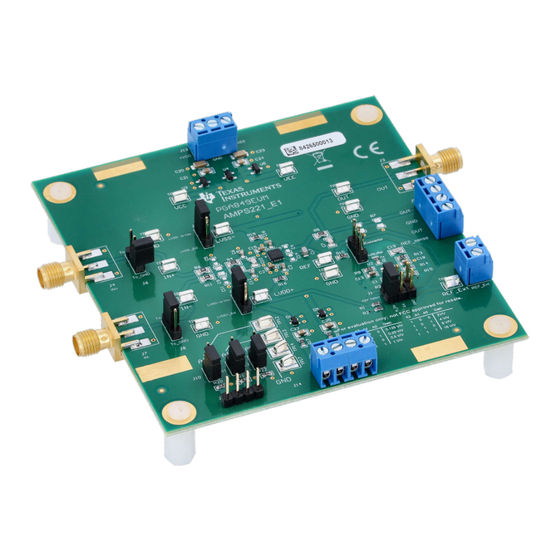
EVM User's Guide: PGA849EVM
PGA849 Evaluation Module
Description
The
PGA849
is a precision, wide-bandwidth
programmable gain instrumentation amplifier (PGA)
for differential to single ended conversion optimized
to drive high-performance analog-to-digital converters
(ADCs) with sampling rates up to 1 MSPS without
the need for an additional ADC driver. The PGA849
is equipped with eight binary gain settings, from
an attenuating gain of 0.125V/V to a maximum of
16V/V, using three digital gain-selection pins. The
device features super-beta input transistors from
Texas Instruments, which provide ultra-low input offset
voltage, offset drift, low input bias current, input
voltage noise, and current noise.
Features
•
Quick and simple evaluation of PGA849; provides
access to features and measures performance
SBOU315 – MARCH 2024
Submit Document Feedback
•
PGA can be configured with binary gain settings
from 0.125V/V to 16V/V
•
Provides three shunt jumpers to set the PGA849
gain-control selection pins
•
Sub-miniature version A (SMA) connectors and
test points allow for quick tests
•
Evaluation board incorporates an optional REF pin
op-amp buffer for flexibility
•
Independent input and output power supply
connections to allow for ADC input overdrive
protection
Applications
•
Factory automation and control
•
Analog input module
•
Data acquisition
•
Test and measurement
•
Semiconductor test
Copyright © 2024 Texas Instruments Incorporated
Description
PGA849 Evaluation Module
1
Advertisement
Table of Contents

Related Manuals for Texas Instruments PGA849


Summary of Contents for Texas Instruments PGA849
- Page 1 (ADCs) with sampling rates up to 1 MSPS without • Evaluation board incorporates an optional REF pin the need for an additional ADC driver. The PGA849 op-amp buffer for flexibility is equipped with eight binary gain settings, from •...
-
Page 2: Kit Contents
The EVM is built with the PGA849RGT device in the 16-pin VQFN package with the thermal pad. This EVM provides access to the features and measures the performance of the PGA849 device. The PGA849 is equipped with eight binary gain settings, from an attenuating gain of 0.125V/V to a maximum of 16V/V, using three digital gain selection pins. - Page 3 The PGA849 incorporates features that simplify interfacing to a single-ended or pseudo-differential input ADC. The REF pin sets the reference point for the output voltage of the PGA849. The REF pin must be driven with a low-impedance source, and the evaluation board provides an optional buffer (U2) to drive the REF pin.
-
Page 4: Jumper Settings
Shunt 1-2: Sets A1 to VCC or 1 Open: Sets A0 to GND or 0 PGA gain CTRL A0 Open Shunt 1-2: Sets A0 to VCC or 1 PGA849 Evaluation Module SBOU315 – MARCH 2024 Submit Document Feedback Copyright © 2024 Texas Instruments Incorporated... -
Page 5: Power Supply Connections
J14.4 Ground By default, the output-stage supply-voltage levels (+LVDD and –LVSS) are set to the PGA849 positive (+VCC) and negative (–VEE) supplies, respectively. The +LVDD pin is connected to +VCC through jumper J9 1-2, and the –LVSS pin is connected to –VEE through J16 1-2. Screw terminal connector J14 provides access to the output-stage supply pins. - Page 6 100 nF LVDD+ 36 V VCC+ LVSS– VEE– TP16 100 nF 36 V 10 µF 100 nF LVSS– Figure 2-3. PGA849EVM Voltage Supply Connections PGA849 Evaluation Module SBOU315 – MARCH 2024 Submit Document Feedback Copyright © 2024 Texas Instruments Incorporated...
- Page 7 REF pin through screw-terminal connector J5.1, and test point TP7 located at the right of the board. The PGA849 output amplifier connection is provided through screw-terminal connector J5.4, SMA connector J3, and test point TP5, located at the right side of the EVM.
-
Page 8: Reference Input
2.5 Reference Input The output voltage of the PGA849 is developed with respect to the voltage on reference pin REF. Use the REF pin to offset the output signal to a precise voltage level. Typically, this offset is set to the mid-voltage level of the output-stage supplies. - Page 9 The PGA849 provides eight binary gain settings, from an attenuating gain of 0.125V/V to a maximum of 16V/V. The gain is controlled by three digital selection pins: A0, A1, and A2. By default, the PGA849 is configured to a gain of 0.125V/V.
- Page 10 For flexibility, the EVM provides optional capacitors C4 and C14. These capacitors are in parallel with the PGA849 output-stage difference amplifier internal resistors to implement noise filtering. In addition, the evaluation board provides footprints R6, R11, C9, C5, and C11 for optional input low-pass filters, and footprints for load resistor R7.
- Page 11 0 R18 10uF 100nF LVSS-_ext 0 R19 LVSS- to Ext BAT854SWF OSTTE040161 100nF TP17 Note: DNP components are not populated. Figure 3-1. PGA849EVM Schematic SBOU315 – MARCH 2024 PGA849 Evaluation Module Submit Document Feedback Copyright © 2024 Texas Instruments Incorporated...
-
Page 12: Pcb Layout
The third internal layer and bottom layer route the input stage power supplies and the output-stage supply connections. Figure 3-2. Top Overlay PCB Layout PGA849 Evaluation Module SBOU315 – MARCH 2024 Submit Document Feedback Copyright © 2024 Texas Instruments Incorporated... - Page 13 Hardware Design Files Figure 3-3. Top Layer PCB Layout Figure 3-4. Ground Layer PCB Layout SBOU315 – MARCH 2024 PGA849 Evaluation Module Submit Document Feedback Copyright © 2024 Texas Instruments Incorporated...
- Page 14 Hardware Design Files www.ti.com Figure 3-5. Power Layer PCB Layout Figure 3-6. Bottom Layer PCB Layout PGA849 Evaluation Module SBOU315 – MARCH 2024 Submit Document Feedback Copyright © 2024 Texas Instruments Incorporated...
- Page 15 RES, 100, 0.1%, 0.125 W, 0805 0805 RT0805BRD07100RL Yageo America R6, R11 RES, 0, 5%, 0.125 W, AEC-Q200 Grade 0, 0805 0805 ERJ-6GEY0R00V Panasonic SBOU315 – MARCH 2024 PGA849 Evaluation Module Submit Document Feedback Copyright © 2024 Texas Instruments Incorporated...
- Page 16 4.5V to 36V, -40℃ to 125℃, 8-Pin SOT-23 (DBV), Green (RoHS & no Sb/Br), Tape and Reel U3, U4, U5 Surge Protection Device in SOT-23 Package SOT23-3 TSM36ADBZR Texas Instruments PGA849 Evaluation Module SBOU315 – MARCH 2024 Submit Document Feedback Copyright © 2024 Texas Instruments Incorporated...
-
Page 17: Additional Information
Newer revisions are available from the TI website at https://www.ti.com/, or call the Texas Instruments Literature Response Center at (800) 477-8924 or the Product Information Center at (972) 644-5580. When ordering, identify the document by both title and literature number. - Page 18 STANDARD TERMS FOR EVALUATION MODULES Delivery: TI delivers TI evaluation boards, kits, or modules, including any accompanying demonstration software, components, and/or documentation which may be provided together or separately (collectively, an “EVM” or “EVMs”) to the User (“User”) in accordance with the terms set forth herein.
- Page 19 www.ti.com Regulatory Notices: 3.1 United States 3.1.1 Notice applicable to EVMs not FCC-Approved: FCC NOTICE: This kit is designed to allow product developers to evaluate electronic components, circuitry, or software associated with the kit to determine whether to incorporate such items in a finished product and software developers to write software applications for use with the end product.
- Page 20 www.ti.com Concernant les EVMs avec antennes détachables Conformément à la réglementation d'Industrie Canada, le présent émetteur radio peut fonctionner avec une antenne d'un type et d'un gain maximal (ou inférieur) approuvé pour l'émetteur par Industrie Canada. Dans le but de réduire les risques de brouillage radioélectrique à...
- Page 21 www.ti.com EVM Use Restrictions and Warnings: 4.1 EVMS ARE NOT FOR USE IN FUNCTIONAL SAFETY AND/OR SAFETY CRITICAL EVALUATIONS, INCLUDING BUT NOT LIMITED TO EVALUATIONS OF LIFE SUPPORT APPLICATIONS. 4.2 User must read and apply the user guide and other available documentation provided by TI regarding the EVM prior to handling or using the EVM, including without limitation any warning or restriction notices.
- Page 22 Notwithstanding the foregoing, any judgment may be enforced in any United States or foreign court, and TI may seek injunctive relief in any United States or foreign court. Mailing Address: Texas Instruments, Post Office Box 655303, Dallas, Texas 75265 Copyright © 2023, Texas Instruments Incorporated...
- Page 23 TI products. TI’s provision of these resources does not expand or otherwise alter TI’s applicable warranties or warranty disclaimers for TI products. TI objects to and rejects any additional or different terms you may have proposed. IMPORTANT NOTICE Mailing Address: Texas Instruments, Post Office Box 655303, Dallas, Texas 75265 Copyright © 2024, Texas Instruments Incorporated...
Need help?
Do you have a question about the PGA849 and is the answer not in the manual?
Questions and answers