Table of Contents
Advertisement
Quick Links
Advertisement
Table of Contents

Subscribe to Our Youtube Channel
Related Manuals for unicore UM982


Summary of Contents for unicore UM982
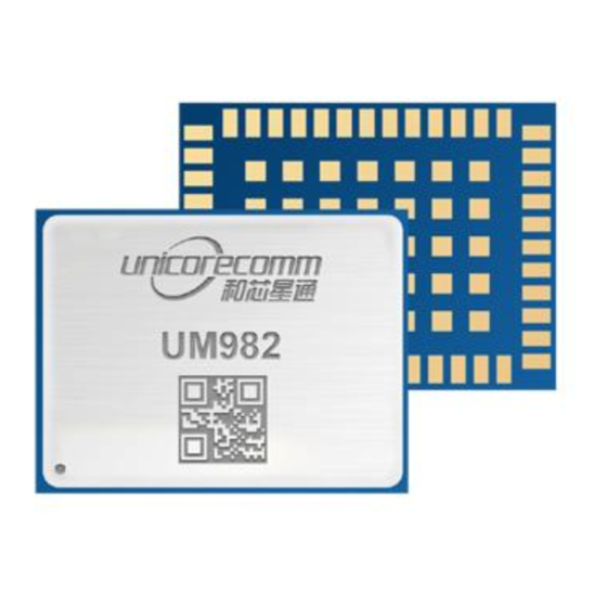
- Page 1 INSTALLATION AND OPERATION USER MANUAL WWW.UNICORECOMM.COM UM982 GPS/BDS/GLONASS/Galileo/QZSS All-constellation Multi-frequency High Precision Positioning & Heading Module Copyright© 2009-2023, Unicore Communications, Inc. Data subject to change without notice.
- Page 2 Revision History Version Revision History Date R1.0 First release 2022-05-19 Table 2-1: Update the description of V_BCKP pin; Chapter 3.3: Add requirement of V_BCKP; Chapter 1.3: Add the description of external interfaces; Add chapter 3.1: Recommended Minimal Design; R1.1 Table 2-4: Update the IO threshold; 2022-09-09 3.2 Antenna Feed Design: D1 and D4 should support high frequency signals (above 2000 MHz);...
- Page 3 Information, such as product specifications, descriptions, features and user guide in this manual, are subject to change by Unicore at any time without prior notice, which may not be completely consistent with such information of the specific product you purchase.
- Page 4 Foreword This document describes the information of the hardware, package, specification and the use of Unicore UM982 module. Target Readers This document applies to technicians who possess the expertise on GNSS receivers.
-
Page 5: Table Of Contents
UM982 User Manual Contents Introduction ....................1 Key Features ........................2 Key Specifications ......................2 Block Diagram ........................5 Hardware ....................6 Pin Definition ........................6 Electrical Specifications ....................9 2.2.1 Absolute Maximum Ratings ..................9 2.2.2 Operating Conditions ....................10 2.2.3 IO Threshold ....................... -
Page 6: Introduction
L1/L2/L5. The module is mainly used in UAVs, lawn mowers, precision agriculture, and intelligent driving. With the support of on-chip RTK positioning and dual-antenna heading solution, UM982 can be used as a rover or base station. UM982 is based on NebulasⅣ... -
Page 7: Key Features
UM982 User Manual 1.1 Key Features 16 mm 21 mm mm, surface-mount device × × Supports all-constellation multi-frequency on-chip RTK positioning and dual- antenna heading solution Supports BDS B1I/B2I/B3I + GPS L1/L2/L5 + GLONASS G1/G2 + Galileo... - Page 8 Power Consumption 600 mW Performance Single Point Horizontal: 1.5 m Positioning Vertical: 2.5 m (RMS) Horizontal: 0.4 m + 1ppm Positioning Accuracy DGPS (RMS) Vertical: 0.8 m + 1ppm Horizontal: 0.8 cm + 1 ppm 3, 4 RTK (RMS) Vertical: 1.5 cm + 1 ppm Observation Accuracy (RMS) GLONASS Galileo...
- Page 9 UM982 User Manual Initialization Time < 5 s (Typical) Initialization Reliability > 99.9% 20 Hz Positioning & Heading Data Update Rate 20 Hz Raw Data observation Differential Data RTCM 3.X Data Format NMEA-0183, Unicore Physical Characteristics Package 48 pin LGA Dimensions 21 mm ×...
-
Page 10: Block Diagram
It integrates a dual-core CPU, a high speed floating point processor and an RTK co-processor, which can fulfill the high precision baseband processing and RTK positioning/heading independently. External Interfaces The external interfaces of UM982 include UART, I , SPI , CAN , PPS, EVENT, RTK_STAT, PVT_STAT, ERR_STAT, RESET_N, etc. -
Page 11: Hardware
UM982 User Manual 2 Hardware 2.1 Pin Definition TXD2 Top View RXD2 TXD1 RXD1 RTK_STAT PVT_STAT ERR_STAT Figure 2-1 UM982 Pin Definition Table 2-1 Pin Description Description — Ground ANT1_IN GNSS master antenna signal input — Ground — Ground When the main power supply VCC is cut off, V_BCKP supplies power to RTC and relevant register. - Page 12 Description ground or leave it floating. SPIS_CSN Chip select pin for SPI slave Master Out / Slave In. This pin is used to receive SPIS_MOSI data in slave mode. SPIS_CLK Clock input pin for SPI slave Master In / Slave Out. This pin is used to transmit SPIS_MISO data in slave mode.
- Page 13 UM982 User Manual Description POWER Power supply (+3.3 V) Built-in function; recommended to add a through- hole testing point and a 10 kΩ pull-up resistor; — cannot connect ground or power supply, cannot input/output data, and cannot be floating Built-in function; recommended to add a through- hole testing point and a 10 kΩ...
-
Page 14: Electrical Specifications
Description — Reserved, floating — Ground — Reserved, floating — Ground — Reserved, floating — Reserved, floating — Reserved, floating 2.2 Electrical Specifications 2.2.1 Absolute Maximum Ratings Table 2-2 Absolute Maximum Ratings Parameter Symbol Min. Max. Unit Power Supply Voltage -0.3 Input Voltage -0.3... -
Page 15: Operating Conditions
UM982 User Manual 2.2.2 Operating Conditions Table 2-3 Operating Conditions Parameter Symbol Min. Typ. Max. Unit Condition Power Supply Voltage Maximum VCC Ripple Working Current VCC=3.3 V Operating Temperature ° C Power Consumption 2.2.3 IO Threshold Table 2-4 IO Threshold... -
Page 16: Dimensions
2.3 Dimensions Table 2-6 Dimensions Parameter Min. (mm) Typ. (mm) Max. (mm) 20.80 21.00 21.50 15.80 16.00 16.50 2.40 2.60 2.80 2.78 2.88 2.98 0.95 1.05 1.15 1.55 1.65 1.75 1.17 1.27 1.37 0.70 0.80 0.90 1.40 1.50 1.60 4.10 4.20 4.30 3.70... - Page 17 UM982 User Manual Figure 2-2 UM982 Mechanical Dimensions Hardware UC-00-M31 EN R1.2...
-
Page 18: Hardware Design
3 Hardware Design 3.1 Recommended Minimal Design ANT2 ANT1 3.3V 3.3V 3.3V ANT_BIAS1 ANT_BIAS2 V_BCKP BIF BIF ANT1_IN RXD(UART) TXD(UART) ANT2_IN RESET_N Figure 3-1 Recommended Minimal Design L1: 68 nH RF inductor in 0603 package is recommended C1: 100 nF + 100 pF capacitors connected in parallel is recommended C2: 100 pF capacitor is recommended C3: N * 10 μF + 1 * 100 nF capacitors connected in parallel is recommended, and the total inductance should be no less than 30 μF... -
Page 19: Antenna Feed Design
ANT1 ANT1_BIAS ANT2_BIAS ANT1_IN ANT2_IN Figure 3-2 UM982 External Antenna Feed Reference Circuit Notes: L1 and L2: feed inductor, 68 nH RF inductor in 0603 package is recommended C1and C3: decoupling capacitor, recommended to connect two capacitors of 100 nF / 100 pF in parallel ... -
Page 20: Power-On And Power-Off
3.3 Power-on and Power-off The VCC initial level when power-on should be less than 0.4 V. The VCC ramp when power-on should be monotonic, without plateaus. The voltages of undershoot and ringing should be within 5% VCC. VCC power-on waveform: The time interval from 10% rising to 90% must be within ... -
Page 21: Recommended Pcb Package Design
UM982 User Manual The 35 pads in the rectangle in Figure 3-3 are for grounding and heat dissipation. In the PCB design, the pads should be connected to a large sized ground to strengthen the heat dissipation. 3.5 Recommended PCB Package Design See the following figure for the recommended PCB package design. -
Page 22: Production Requirement
4 Production Requirement Recommended soldering temperature curve is as follows: Rising Preheating Reflux Cooling ° C Peak 245 ° C 40~60s 60~120s Max. 4° C/s Max. 3° C/s Time (s) Figure 4-1 Soldering Temperature (Lead-free) Temperature Rising Stage Rising slope: Max. 3 ° C/s ... -
Page 23: Packaging
Figure 5-1 Label Description 5.2 Product Packaging The UM982 module uses carrier tape and reel (suitable for mainstream surface mount devices), packaged in vacuum-sealed aluminum foil antistatic bags, with a desiccant inside to prevent moisture. When using reflow soldering process to solder modules, please strictly comply with IPC standard to conduct temperature and humidity control. - Page 24 Figure 5-2 UM982 Package Reel Feed Direction Cover Tape Carrier Tape Dimensions 0.35 1.75± 0.10 20.20± 0.10 40.40± 0.10 330*100*44 2.00± 0.10 16.8 1.50 ± 0.10 0.00 +0.10 1.50 4.00± 0.10 -0.00 40.00± 0.20 10Po 44.00± 0.30 C(3:1) 24.00± 0.10 Note: 16.80±...
- Page 25 Figure 5-4 Normal Humidity Indication Figure 5-5 Abnormal Humidity Indication The UM982 is rated at MSL level 3. Please refer to the IPC/JEDEC J-STD-033 standards for the package and operation requirements. You may access to the website www.jedec.org to get more information.
- Page 26 和芯星通科技(北京)有限公司 Unicore Communications, Inc. 北京市海淀区丰贤东路 7 号北斗星通大厦三层 F3, No.7, Fengxian East Road, Haidian, Beijing, P.R.China, 100094 www.unicorecomm.com Phone: 86-10-69939800 Fax: 86-10-69939888 info@unicorecomm.com www.unicorecomm.com...
Need help?
Do you have a question about the UM982 and is the answer not in the manual?
Questions and answers