
Related Manuals for unicore UM670A


Summary of Contents for unicore UM670A
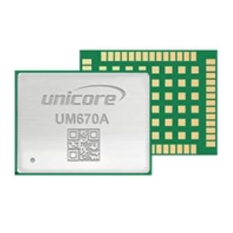
- Page 1 HARDWARE REFERENCE DESIGN WWW.UNICORE.COM UM670A Automotive-grade GNSS Navigation and Positioning Module Copyright© 2009-2024, Unicore Communications, Inc. Data subject to change without notice.
-
Page 2: Revision History
This manual does not represent, and in any case, shall not be construed as a commitments or warranty on the part of Unicore with respect to the fitness for a particular purpose/use, the accuracy, reliability and correctness of the information contained herein. -
Page 3: Target Readers
Foreword This document describes the hardware reference design of Unicore UM670A module. This is only a draft version, for reference only. Target Readers This document applies to technicians who are familiar with GNSS receivers. -
Page 4: Table Of Contents
Contents Block Diagram ................... 1 UM670A Peripheral Design ............... 2 Main Power VCC ......................4 Backup Battery V_BCKP ....................4 Active Antenna Feed Circuit .................... 5 Antenna Detection Circuit ....................6 Reset Circuit ........................6 Appendix: Schematics of Reference Design ..........6... -
Page 5: Block Diagram
UART Interface RESET_N Filter ANT1_IN L5/L2 D_SEL GNSS GNSS CLOCK TCXO Figure 1-1 UM670A Block Diagram Different sub models support different frequencies. Table 1-1 UM670A Frequency Description Sub-model Frequency UM670A-03 L1+L5 UM670A-23 L1+L2 or L1+L5 UM670A-12 L1 or L1+L5 The antenna detection, SPIM and UART2 are supported by hardware version V1.1 and above. SPIS shares the pins with I C/UART1. -
Page 6: Um670A Peripheral Design
2 UM670A Peripheral Design Connect the ANT_IN signal to the antenna, and note the 50 Ω impedance matching. Connect all the GND pins to the ground. Leave the IO pin open if not used Recommended to add TVS anti-surge protection at the input of the module. - Page 7 UM670A Hardware Reference Design UM670A RF Line R0805 UM670A Module Note: PINs leave OPEN if not used Figure 2-1 UM670A Peripheral Design UC-08-M62 EN R1.0 UM670A Peripheral Design...
-
Page 8: Main Power Vcc
500 ms. Backup Battery V_BCKP When using the hot start function of the module UM670A, you need to provide backup power for the module. The input range of V_BCKP is 2.0 V to 3.6 V. -
Page 9: Active Antenna Feed Circuit
UM670A Hardware Reference Design When you do not use the hot start function, connect V_BCKP to VCC or a standalone power source. Do not connect it to ground or leave it floating. Active Antenna Feed Circuit The antenna feed circuit consists of the anti-surge design, filter inductors, and ESD protection. -
Page 10: Antenna Detection Circuit
ANT_OFF Open Short Reset Circuit UM670A supports system reset. The pin RESET_N is active low and the active time should be no less than 5 ms. 3 Appendix: Schematics of Reference Design Supported by specific version. Appendix: Schematics of Reference Design... - Page 11 UM670A Hardware Reference V_ANT +3.3 V STATUS ANT_DETECT ANT_SHORT_N ANT_OFF OPEN SHORT ANT DETECT Note: I/O Buffer is required when V_ANT&VCCIN voltage not matched UM670A RF Line UM670A R0805 Unicore Com munications,Inc Title Title Title UM670A-REF UM670A Module Note: PINs leave OPEN if not used...
- Page 12 和芯星通科技(北京)有限公司 Unicore Communications, Inc. 北京市海淀区丰贤东路 7 号北斗星通大厦三层 F3, No.7, Fengxian East Road, Haidian, Beijing, P.R.China, 100094 www.unicore.com Phone: 86-10-69939800 Fax: 86-10-69939888 info@unicorecomm.com www.unicore.com...
Need help?
Do you have a question about the UM670A and is the answer not in the manual?
Questions and answers