Table of Contents
Advertisement
Quick Links
Advertisement
Table of Contents

Related Manuals for Supermicro SUPERO PDSBA+


Summary of Contents for Supermicro SUPERO PDSBA+
- Page 1 PDSBA+ PDSBA PDSBE USER’S MANUAL Revision 1.0a...
- Page 2 Clara County in the State of California, USA. The State of California, County of Santa Clara shall be the exclusive venue for the resolution of any such disputes. Supermicro's total liability for all claims will not exceed the price paid for the hardware product.
-
Page 3: Manual Organization
Intel Virtualization Technology (VT), Streaming SIMD Extensions 2 (SSE2), Streaming SIMD Extensions 3 (SSE3), Execute Disable (XD) Bit. Please refer to the motherboard specifi cations pages on our web site (http://www.supermicro.com/ Product_page/product-m.htm) for updates on supported processors. This product is intended to be professionally installed. -
Page 4: Table Of Contents
Manual Organization ....................iii Conventions Used in the Manual .................. iii Chapter 1: Introduction Overview ......................1-1 Checklist ..................... 1-1 Contacting Supermicro ................1-2 PDSBA+/PDSBA/PDSBE Image ..........1-3 PDSBA+/PDSBA/PDSBE Layout ..........1-4 PDSBA+/PDSBA/PDSBE Quick Reference ........ 1-5 Motherboard Features ................1-6 Intel's G965/P965 Chipset: System Block Diagram ........ - Page 5 Table of Contents Fan Headers ..................... 2-13 ATX PS/2 Keyboard and PS/2 Mouse Ports ..........2-14 Serial Ports ....................2-14 Wake-On-Ring ..................2-15 Wake-On-LAN ..................2-15 GLAN1 Port ....................2-16 Speaker Connector .................. 2-16 High Defi nition Audio (HDA) ..............2-17 CD Header/Auxiliary Audio Header ............
- Page 6 PDSBA+/PDSBA/PDSBE User’s Manual Chapter 4: BIOS Introduction ....................... 4-1 Running Setup ....................4-2 Main BIOS Setup ..................... 4-2 Advanced Setup ....................4-5 Security Setup ....................4-16 Boot Setup ...................... 4-18 Exit ........................4-19 Appendices: Appendix A: BIOS POST Messages .................A-1 Appendix B: BIOS POST Codes ................B-1 Appendix C: Software Installation Instructions ............C-1...
-
Page 7: Chapter 1: Introduction
Checklist Congratulations on purchasing your computer motherboard from an acknowledged leader in the industry. Supermicro boards are designed with the utmost attention to detail to provide you with the highest standards in quality and performance. Please check that the following items have all been included with your motherboard. -
Page 8: Contacting Supermicro
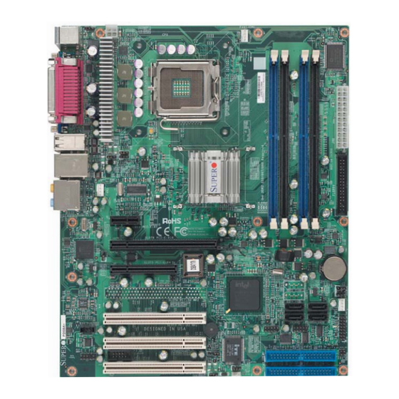
PDSBA+/PDSBA/PDSBE User’s Manual Contacting Supermicro Headquarters Address: SuperMicro Computer, Inc. 980 Rock Ave. San Jose, CA 95131 U.S.A. Tel: +1 (408) 503-8000 Fax: +1 (408) 503-8008 Email: marketing@supermicro.com (General Information) support@supermicro.com (Technical Support) Web Site: www.supermicro.com Europe Address: SuperMicro Computer B.V. - Page 9 Chapter 1: Introduction PDSBA/PDSBE Image PDSBA+ Image...
- Page 10 PDSBA+/PDSBA/PDSBE User’s Manual Motherboard Layout (not drawn to scale) JPWAKE 4-PinPWR KB/MS Processor 965P USB3/4/5/6 USB1/2 (North Bridge) Clock Slot7 PCI-E x1 Slot6 PCI-E x16 CTRL J B T 1 Battery F W H Slot5 PCI-E x4 ICH8 J P 3 J W D Slot4 JLED...
-
Page 11: Pdsba+/Pdsba/Pdsbe Quick Reference
Chapter 1: Introduction PDSBA+/PDSBA/PDSBE Quick Reference Jumpers Description Default Setting JBT1 CMOS Clear (*See Chapter 2) JFSB1/JFSB2 CPU Frequency Pins 1-2/Pins 1-2(Auto) JI 2 C1/JI 2 C2 SMB to PCI Slots Open/Open (Disabled) JP2 (*PDSBA+ only) ITE IDE Enabled Pins 1-2 (Enabled) JP3 (*PDSBA+/PDSBA) Trust Platform Module Enable Pins 1-2 (Enabled) JPL1 Giga-bit LAN Enable... -
Page 12: Motherboard Features
PDSBA+/PDSBA/PDSBE User’s Manual Motherboard Features Latest CPU technology! ® ® • Single Intel dual-core E6000/Xeon 3000/Pentium D/Pentium 4/Celeron Pro- cessor with a system bus speed of 1066/800/533 MHz • Supports Intel EM64T, Enhanced Intel SpeedStep (EIST), Intel Virtualization Technology (VT) Streaming SIMD Extensions 2 &... - Page 13 If this occurs, revert the setting to the default setting. In addition, extra fans may be needed for proper system cooling. The PDSBA+/PDSBA/PDSBE offers the option of "overclocking"; however, Supermicro is not responsible for any damage caused by use of overclocking.
- Page 14 PDSBA+/PDSBA/PDSBE User’s Manual Figure 1-3. The G965/P965 Chipset: System Block Diagram Note: This is a general block diagram and may not exactly represent the features on your motherboard. See the following pages for the actual specifi cations of each motherboard. (*Note: Integrated Graphics is not available for the P965 Chipset.)
-
Page 15: Chipset Overview
Chapter 1: Introduction Chipset Overview Intel’s G965/P965 Chipset is specially designed for use with dual core processors. It consists of two primary components: the Graphic Memory Controller Hub (GMCH)/ Memory Controller Hub (MCH) and the I/O Controller Hub (ICH8). Optimized for the dual-core E6000/Xeon 3000/Pentium ®... -
Page 16: Pc Health Monitoring
PDSBA+/PDSBA/PDSBE User’s Manual 1-3 PC Health Monitoring This section describes the PC health monitoring features of the PDSBA+/PDSBA/ PDSBE. The motherboard has an onboard System Hardware Monitor chip that supports PC health monitoring. Onboard Voltage Monitors for the CPU Core, +1.8V, +3.3V, +3.3V standby, +5V, Vbat and ±12V The onboard voltage monitor will scan these voltages continuously. -
Page 17: Power Supply
Chapter 1: Introduction Main Switch Override Mechanism When an ATX power supply is used, the power button can function as a system suspend button. When the user presses the power button, the system will enter a SoftOff state. The monitor will be suspended and the hard drive will spin down. Pressing the power button again will cause the whole system to wake-up. -
Page 18: Super I/O
PDSBA+/PDSBA/PDSBE User’s Manual Super I/O The disk drive adapter functions of the Super I/O chip include a fl oppy disk drive controller that is compatible with industry standard 82077/765, a data separator, write pre-compensation circuitry, decode logic, data rate selection, a clock genera- tor, drive interface control logic and interrupt and DMA logic. -
Page 19: Chapter 2: Installation
Chapter 2: Installation Chapter 2 Installation Static-Sensitive Devices Electric-Static-Discharge (ESD) can damage electronic com ponents. To prevent damage to your system board, it is important to handle it very carefully. The following measures are generally suffi cient to protect your equipment from ESD. Precautions •... -
Page 20: Processor And Heatsink Installation
PDSBA+/PDSBA/PDSBE User's Manual Processor and Heatsink Fan Installation When handling the processor package, avoid placing direct pressure on the label area of the fan. *Notes: 1. Always connect the power cord last and always remove it before adding, removing or changing any hardware components. Make sure that you install the processor into the CPU LGA 775 socket before you install the CPU heatsink. - Page 21 Chapter 2: Installation North Center Edge 3. Use your thumb and your index fi nger to hold the CPU at the North Center Edge and the South Center Edge of the CPU. 4. Align CPU Pin1 (the CPU corner marked with a triangle) against the socket corner that is marked with a triangle cutout.
- Page 22 PDSBA+/PDSBA/PDSBE User's Manual Installing DIMMs Note: Check the Supermicro web site for recommended memory modules. CAUTION Exercise extreme care when installing or removing DIMM modules to prevent any possible damage. Also note that the memory is interleaved to improve performance (see step 1).
- Page 23 Chapter 2: Installation Figure 2-2. Installing and Removing DIMMs DDR BD D DDR2 F W H To Install: Insert module vertically and press down until it snaps into place. Pay attention to the alignment notch at the bottom. To Remove: Use your thumbs DDR BD S Top View of DDR2...
-
Page 24: Control Panel Connectors/Io Ports
PDSBA+/PDSBA/PDSBE User's Manual Control Panel Connectors/IO Ports The I/O ports are color coded in conformance with the PC 99 specifi cation. See Figure 2-3 below for the colors and locations of the various I/O ports. A. Back Panel Connectors/IO Ports F W H Figure 2-3. -
Page 25: Front Control Panel
These connectors are designed specifi - cally for use with Supermicro server chassis. See Figure 2-4 for the descriptions of the various control panel buttons and LED indicators. Refer to the following section for descriptions and pin defi... -
Page 26: Front Control Panel Pin Defi Nitions
PDSBA+/PDSBA/PDSBE User's Manual C. Front Control Panel Pin Defi nitions Power LED Power LED Pin Defi nitions (JF1) The Power LED connection is located Pin# Defi nition on pins 15 and 16 of JF1. Refer to the LED_Anode table on the right for pin defi nitions. PWR LED Signal HDD LED The HDD LED connection is located... -
Page 27: Oh/Fan Fail Led
Chapter 2: Installation NIC1 Indicator GLAN1/2 LED Pin Defi nitions (JF1) The NIC (Network Interface Control- Pin# Defi nition ler) LED connection for GLAN port1 LED_Anode is located on pins 11 and 12 of JF1 . NIC1 LED Attach the NIC LED cables to display Signal network activity. -
Page 28: Reset Button
PDSBA+/PDSBA/PDSBE User's Manual Reset Button Reset Button Pin Defi nitions (JF1) The Reset Button connection is located Pin# Defi nition on pins 3 and 4 of JF1. Attach it to the hardware reset switch on the computer Reset case. Refer to the table on the right for Ground pin defi... -
Page 29: Connecting Cables
Chapter 2: Installation ATX Power 24-pin Connector Connecting Cables Pin Defi nitions Pin# Defi nition Pin # Defi nition ATX/Auxiliary Power +3.3V +3.3V Connectors -12V +3.3V There are a 24-pin main power PS_ON connector (J40) and a 4-pin power connector (J41) on the motherboard. These power connectors meet the SSI EPS 12V specifi... -
Page 30: Universal Serial Bus (Usb)
PDSBA+/PDSBA/PDSBE User's Manual Back Panel USB Universal Serial Bus (USB) Pin# Defi nitions There are ten USB 2.0 (Universal Serial Bus) ports/headers on the motherboard. Six of them are Back Panel USB ports (USB#1/2: J11, Ground USB#3/4/5/6: J43), and the other four are Front Panel USB headers (USB#7/8:J44, USB#9/10:J45). -
Page 31: Fan Headers
Chapter 2: Installation Fan Headers Fan Header Pin Defi nitions The PDSBA+/PDSBA/PDSBE has three Pin# Defi nition chassis fan headers (Fan1 to Fan3). Fan Ground 1 is the CPU Fan. Fan 2 and Fan 3 are +12V system/chassis fans. (*Note: all these Tachometer fans are 4-pin fans. -
Page 32: Atx Ps/2 Keyboard And Ps/2 Mouse Ports
PDSBA+/PDSBA/PDSBE User's Manual ATX PS/2 Keyboard and PS/2 Keyboard and Mouse Port Pin PS/2 Mouse Ports Defi nitions The ATX PS/2 keyboard and the PS/2 Pin# Defi nition mouse are located at J28. See the Data table on the right for pin defi nitions. (The mouse port is above the key- Ground board port. -
Page 33: Wake-On-Ring
Chapter 2: Installation Wake-On-Ring Wake-On-Ring The Wake-On-Ring header is desig- Pin Defi nitions (JWOR) nated JWOR. This function allows Pin# Defi nition your computer to receive and be Ground "waken up" by an incoming call to Wake-up the modem when the system is in the suspend state. -
Page 34: Speaker Connector
PDSBA+/PDSBA/PDSBE User's Manual GLAN 1 (Giga-bit Ethernet Port) A G-bit Ethernet port is located at J11 GLAN1 on the IO backplane. This port ac- cepts RJ45 type cables. Speaker Speaker Connector A Speaker/Buzzer header (J9) is located on the motherboard. Pin Setting Defi... -
Page 35: High Defi Nition Audio (Hda)
Chapter 2: Installation High Defi nition Audio (HDA) Orange: The PDSBA+/PDSBA/PDSBE features a Blue: Line-In CEN/LFE 7.1+2 Channel High Defi nition Audio (HDA) (J46) codecs that provides 10DAC channels, Black: Back Green:Front Surround simultaneously supporting 7.1 sound playback, plus 2 channels of independent Grey: Side Pink: Mic-In Surround... -
Page 36: Jumper Settings
PDSBA+/PDSBA/PDSBE User's Manual Jumper Settings Explanation of Jumpers Connector Pins To modify the operation of the motherboard, jumpers can be used to choose between optional settings. Jumper Jumpers create shorts between two pins to change the function of the connector. Pin 1 is identifi ed with a Setting square solder pad on the printed circuit Pin 1-2 short... -
Page 37: Cmos Clear
Chapter 2: Installation CMOS Clear JBT1 is used to clear CMOS. Instead of pins, this "jumper" consists of contact pads to prevent the accidental clearing of CMOS. To clear CMOS, use a metal object such as a small screwdriver to touch both pads at the same time to short the connection. - Page 38 PDSBA+/PDSBA/PDSBE User's Manual CPU Front Side Bus Speed CPU FSB Jumper Settings JFSB1 and JFSB2 allow you to set the JFSB2 JFSB1 Frequency Front Side Bus Frequency. See the table *Auto on the right for pin defi nitions. (*Default 266MHz is Auto.) Open 200MHz...
-
Page 39: Usb Wake-Up
Chapter 2: Installation USB Wake-Up JPUSB1 (Back Panel USB Wake-up) Use JPUSB jumpers to enable the function of "System Wake-Up via USB devices", which al- Pin# Defi nition lows you to "wake-up" the system by pressing Enabled a key on the USB keyboard or by clicking the Disabled (*default) USB mouse of your system. -
Page 40: Ide Enable/Disable
PDSBA+/PDSBA/PDSBE User's Manual IDE Enable/Disable IDE Enable (*PDSBA+ only) Pin# Defi nition JP2 enables or disables IDE#1 and Enabled (*default) IDE#2 on the motherboard. See the Disabled table on the right for jumper settings. The default setting is enabled. TPM Enable (*PDSBA/ TPM Enable PDSBA+ only) JP3 enables or disables Trust Platform... -
Page 41: Keyboard Wake-Up
Chapter 2: Installation Keyboard Wake-Up PS2 Keyboard Wake-up The JPWAKE jumper is used Pin# Defi nition together with the Keyboard Wake- Enabled (*default) Up function in BIOS. Enable both Disabled the jumper and the BIOS setting to allow the user to wake up the system when hitting a key on the keyboard. -
Page 42: Onboard Indicators
PDSBA+/PDSBA/PDSBE User's Manual Onboard Indicators Link Activity GLAN LEDs There is one GLAN port (J11) locat- GLAN Activity Indicator ed above USB Ports 1/2 on the I/O Backpanel. This Gigabit Ethernet LAN Color Status Defi nition port has two LEDs. The green LED indi- Green Flashing Active... -
Page 43: Power Led
Chapter 2: Installation Power LED Power LED Jumper Settings There is an Onboard Power LED (JLED) Jumper Setting Defi nition located on the motherboard. When this Enabled (*Default) LED is lit, the system is on. Be sure to Disabled turn off the system and unplug the power cord before removing or installing com- ponents. -
Page 44: Parallel Port Connector
PDSBA+/PDSBA/PDSBE User's Manual Parallel Port, Floppy Drive and IDE Hard Drive Connections Note the following when connecting the fl oppy and hard disk drive cables: • The fl oppy disk drive cable has seven twisted wires. • A red mark on a wire typically designates the location of pin 1. •... -
Page 45: Floppy Connector
Chapter 2: Installation Floppy Drive Connector Pin Defi nitions (Floppy) Floppy Connector Pin# Defi nition Pin # Defi nition The fl oppy connector is located on Ground FDHDIN J27. See the table below for pin Ground Reserved defi nitions. FDEDIN Ground Index Ground... -
Page 46: Ide Connectors
PDSBA+/PDSBA/PDSBE User's Manual IDE Connectors (*PDSBA+ IDE Connectors Pin Defi nitions only) Pin# Defi nition Pin # Defi nition Reset IDE Ground There are two ITE IDE Connectors on Host Data 7 Host Data 8 the PDSBA+. Be sure to close Pin 1 Host Data 6 Host Data 9 and Pin 2 of JP2 to enable the IDE con-... -
Page 47: Chapter 3: Troubleshooting
Chapter 3: Troubleshooting Chapter 3 Troubleshooting Troubleshooting Procedures Use the following procedures to troubleshoot your system. If you have followed all of the procedures below and still need assistance, refer to the ‘Technical Support Procedures’ and/or ‘Returning Merchandise for Service’ section(s) in this chapter. Always disconnect the AC power cord before adding, changing or installing any hardware components. -
Page 48: Memory Errors
Technical Support Procedures Before contacting Technical Support, please take the following steps. Also, note that as a motherboard manufacturer, Supermicro does not sell directly to end-us- ers, so it is best to fi rst check with your distributor or reseller for troubleshooting services. -
Page 49: Frequently Asked Questions
4. Distributors: For immediate assistance, please have your account number ready when placing a call to our technical support department. We can be reached by e-mail at support@supermicro.com, by phone at:(408) 503-8000, option 2, or by fax at (408)503-8019. Frequently Asked Questions... -
Page 50: Returning Merchandise For Service
PDSBA+/PDSBA/PDSBE User's Manual Question: I installed my microphone correctly but I can't record any sound. What should I do? Answer: Go to <Start>, <Programs>, <Accessories>, <Entertainment> and then <Volume Control>. Under the Properties tab, scroll down the list of devices in the menu and check the box beside "Microphone". -
Page 51: Chapter 4: Bios
Note: Due to periodic changes to the BIOS, some settings may have been added or deleted and might not yet be recorded in this manual. Please refer to the Manual Download area of the Supermicro web site <http://www.supermicro.com> for any changes to the BIOS that may not be refl ected in this manual. -
Page 52: Running Setup
PDSBA+/PDSBA/PDSBE User's Manual Running Setup *Default settings are in bold text unless otherwise noted. The BIOS setup options described in this section are selected by choosing the appropriate text from the main BIOS Setup screen. All displayed text is described in this section, although the screen display is often all you need to understand how to set the options (see next page). - Page 53 Chapter 4: BIOS Main BIOS Setup Menu Main Setup Features System Time To set the system date and time, key in the correct information in the appropriate fi elds. Then press the <Enter> key to save the data. System Date Using the arrow keys, highlight the month, day and year fi...
- Page 54 PDSBA+/PDSBA/PDSBE User's Manual SATA Controller Mode Select Compatible to allow the SATA and PATA drives to be automatically-detected and be placed in the Legacy Mode by the BIOS. Select Enhanced to allow the SATA and PATA drives to be to be automatically-detected and be placed in the Native Mode.
-
Page 55: Advanced Setup
Chapter 4: BIOS Ultra DMA Mode This option allows the user to select Ultra DMA Mode. The options are Disabled, System Memory Mode 0, Mode 1, Mode 2, Mode 3, Mode 4, and Mode 5. This display informs you how much system memory is recognized as being present in the system. - Page 56 PDSBA+/PDSBA/PDSBE User's Manual Quiet Mode This setting allows you to Enable or Disable the graphic logo screen during boot-up. POST Beeps Set to Enabled to activate the alarm if an error occurs during bootup. If set to Disabled, the alarm will not be beeping even if a boot error occurs. ACPI Mode Use the setting to determine if you want to employ ACPI (Advanced Confi...
- Page 57 (*Available when supported by the CPU.) Select enabled to enable CPU Overclocking which will cause the CPU to operate at a higher speed than that is intended . (*Note: Supermicro does not recommend CPU overclocking because it might impede CPU or system stability.) The options are: Disabled, +5%, +10%, +15%, and +20%.
- Page 58 PDSBA+/PDSBA/PDSBE User's Manual Set Maximum Ext. CPUID=3 When set to Enabled, the Maximum Extended CPUID will be set to 3. The options are Disabled and Enabled. Echo TPR Set to Enabled to prevent xTPR messages from being sent to the system. The options are Disabled and Enabled.
- Page 59 Chapter 4: BIOS Clock Spectrum Feature If Enabled, the BIOS will monitor the level of Electromagnetic Interference caused by the components and will attempt to decrease the interference whenever needed. The options are Enabled and Disabled. PCI Express Graphics Port If set to Enabled, the PCI Express Graphics port will always be enabled.
- Page 60 PDSBA+/PDSBA/PDSBE User's Manual Memory Cache Memory Cache This setting allows the user to enable or disable the functions of Memory Cache. The options are Enabled and Disabled. Cache System BIOS Area This setting allows you to designate a reserve area in the system memory to be used as a System BIOS buffer to allow the BIOS write (cache) its data into this reserved memory area.
- Page 61 Chapter 4: BIOS be cached (written) into a buffer, a storage area in the Static DROM (SDROM) or written into L1, L2, L3 cache inside the CPU to speed up CPU operations. Select "Uncached" to disable this function. Select "Write Through" to allow data to be cached into the buffer and written into the system memory at the same time.
- Page 62 PDSBA+/PDSBA/PDSBE User's Manual PCI-E x4 Slot#5 PCI Express Port#1 Select Enabled to always enable PCI-Ex4 Slot 5 and all other PCI-E ports. Select Disabled to disable PCI-Ex4 Slot 5 and all other PCI-E ports. When set to Auto, PCI-Ex4 Slot 5 will be enabled if a PCI add-on card is detected. The options are Auto, Enabled and Disabled.
- Page 63 Chapter 4: BIOS PCI-E x1 NIC PCI Express Port#6 Select Enabled to always enable PCI-Ex1 NIC and all other PCI-E ports. Select Disabled to disable PCI-Ex1 NIC and all other PCI-E ports. When set to Auto, PCI-Ex1 NIC will be enabled if a PCI add-on card is detected. The options are Auto, Enabled and Disabled.
- Page 64 PDSBA+/PDSBA/PDSBE User's Manual I/O Device Confi guration Access the submenu to make changes to the following settings. KBC Clock Input This setting allows you to select clock frequency for KBC. The options are 6MHz, 8MHz, 12MHz, and 16MHz. Serial Port A This setting allows you to assign control of serial port A.
- Page 65 Chapter 4: BIOS Mode This feature allows you to specify the parallel port mode. The options are Output only, Bi-Directional, EPP and ECP. DMA Channel This item allows you to specify the DMA channel for the parallel port. The options are DMA1 and DMA3. Floppy Disk Controller This setting allows you to assign control of the fl...
- Page 66 PDSBA+/PDSBA/PDSBE User's Manual Security Settings Choose Security from the Phoenix BIOS Setup Utility main menu with the arrow keys. You should see the following display. Security setting options are displayed by highlighting the setting using the arrow keys and pressing <Enter>. All Security BIOS settings are described in this section.
- Page 67 Chapter 4: BIOS Fixed Disk Boot Sector Select Normal to enable Write-Protect the boot sector on the hard drives to protect against viruses. Password on Boot This setting allows you to require a password to be entered when the system boots up.
- Page 68 PDSBA+/PDSBA/PDSBE User's Manual Boot Settings Choose Boot from the Phoenix BIOS Setup Utility main menu with the arrow keys. You should see the following display. See details on how to change the order and specs of boot devices in the Item Specifi c Help window. All Boot BIOS settings are described in this section.
-
Page 69: Exit
Chapter 4: BIOS Exit Choose Exit from the Phoenix BIOS Setup Utility main menu with the arrow keys. You should see the following display. All Exit BIOS settings are described in this section. Exit Saving Changes Highlight this item and hit <Enter> to save any changes you made and to exit the BIOS Setup utility. - Page 70 PDSBA+/PDSBA/PDSBE User's Manual Notes 4-20...
-
Page 71: Appendix Abios Post Messages
Appendix A: BIOS POST Messages Appendix A BIOS POST Messages During the Power-On Self-Test (POST), the BIOS will check for problems. If a prob- lem is found, the BIOS will activate an alarm or display a message. The following is a list of such BIOS messages. - Page 72 PDSBA+/PDSBA/PDSBE User's Manual System CMOS checksum bad - Default confi guration used System CMOS has been corrupted or modifi ed incorrectly, perhaps by an application program that changes data stored in CMOS. The BIOS installed Default Setup Values. If you do not want these values, enter Setup and enter your own values.
- Page 73 Appendix A: BIOS POST Messages System cache error - Cache disabled RAM cache failed and BIOS disabled the cache. On older boards, check the cache jumpers. You may have to replace the cache. See your dealer. A disabled cache slows system performance considerably. CPU ID: CPU socket number for Multi-Processor error.
- Page 74 PDSBA+/PDSBA/PDSBE User's Manual Fixed Disk n Fixed disk n (0-3) identifi ed. Invalid System Confi guration Data Problem with NVRAM (CMOS) data. I/O device IRQ confl ict I/O device IRQ confl ict error. PS/2 Mouse Boot Summary Screen: PS/2 Mouse installed. nnnn kB Extended RAM Passed Where nnnn is the amount of RAM in kilobytes successfully tested.
- Page 75 Appendix A: BIOS POST Messages Parity Check 2 nnnn Parity error found in the I/O bus. BIOS attempts to locate the address and display it on the screen. If it cannot locate the address, it displays ????. Press <F1> to resume, <F2> to Setup, <F3> for previous Displayed after any recoverable error message.
- Page 76 PDSBA+/PDSBA/PDSBE User's Manual Notes...
-
Page 77: Appendix Bbios Post Codes
Appendix B: BIOS POST Codes Appendix B BIOS POST Codes This section lists the POST (Power On Self Test) codes for the PhoenixBIOS. POST codes are divided into two categories: recoverable and terminal. Recoverable POST Errors When a recoverable type of error occurs during POST, the BIOS will display an POST code that describes the problem. - Page 78 PDSBA+/PDSBA/PDSBE User's Manual POST Code Description 8254 timer initialization 8237 DMA controller initialization Reset Programmable Interrupt Controller 1-3-1-1 Test DRAM refresh 1-3-1-3 Test 8742 Keyboard Controller Set ES segment register to 4 GB Auto size DRAM Initialize POST Memory Manager Clear 512 kB base RAM 1-3-4-1 RAM failure on address line xxxx* 1-3-4-3 RAM failure on data bits xxxx* of low byte of...
- Page 79 Appendix B: BIOS POST Codes POST Code Description Test RAM between 512 and 640 kB Test extended memory Test extended memory address lines Jump to UserPatch1 Confi gure advanced cache registers Initialize Multi Processor APIC Enable external and CPU caches Setup System Management Mode (SMM) area Display external L2 cache size Load custom defaults (optional)
- Page 80 PDSBA+/PDSBA/PDSBE User's Manual POST Code Description Check for SMART Drive (optional) Set up Power Management Initialize security engine (optional) Enable hardware interrupts Determine number of ATA and SCSI drives Set time of day Check key lock Initialize typematic rate Erase <ESC> prompt Scan for <ESC>...
- Page 81 Appendix B: BIOS POST Codes POST Code Description Unknown interrupt Check Intel Branding string Alert Standard Format initialization Log error if micro-code not updated properly The following are for boot block in Flash ROM POST Code Description Initialize the chipset Initialize the bridge Initialize the CPU Initialize system timer...
- Page 82 PDSBA+/PDSBA/PDSBE User's Manual Notes...
-
Page 83: Appendix C: Software Installation Instructions
Appendix C: Software Installation Instructions Appendix C Software Installation Instructions A. Installing Drivers After you've installed Windows Operating System, a screen as shown below will appear. You are ready to install software programs and drivers that have not yet been installed. To install these software programs and drivers, click the icons to the right of these items. - Page 84 PDSBA+/PDSBA/PDSBE User's Manual B. Confi guring Supero Doctor III The Supero Doctor III program is a Web base management tool that supports remote management capability. It includes Remote and Local Management tools. The local management is called SD III Client. The Supero Doctor III program included on the CDROM that came with your motherboard allows you to moni- tor the environment and operations of your system.
- Page 85 Supero Doctor III Interface Display Screen-II (Remote Control) (*Note: SD III Software Revision 1.0 can be downloaded from our Web site at: ftp://ftp.supermicro.com/utility/Supero_Doctor_III/. You can also download SDIII User's Guide at: http://www.supermicro.com/PRODUCT/Manuals/SDIII/UserGuide. pdf. For Linux, we will still recommend that you use Supero Doctor II.)
- Page 86 PDSBA+/PDSBA/PDSBE User's Manual Notes...
Need help?
Do you have a question about the SUPERO PDSBA+ and is the answer not in the manual?
Questions and answers