Sign In
Upload
Manuals
Brands
Telit Wireless Solutions Manuals
Control Unit
LE910C1-AP
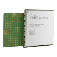
Telit Wireless Solutions LE910C1-AP Manuals
Manuals and User Guides for Telit Wireless Solutions LE910C1-AP. We have
6
Telit Wireless Solutions LE910C1-AP manuals available for free PDF download: Hardware Design Manual, Hardware User's Manual, Hw Design Manual, Thermal Design Manual
Telit Wireless Solutions LE910C1-AP Hardware User's Manual (119 pages)
Brand:
Telit Wireless Solutions
| Category:
Control Unit
| Size: 3 MB
Table of Contents
Table of Contents
5
1 Introduction
13
Scope
13
Audience
13
Contact Information, Support
13
Text Conventions
14
Related Documents
15
Table 2: Related Documents
15
Abbreviations
16
2 General Product Description
17
Overview
17
Applications
17
Table 1: Applicability Table
17
General Functionality and Main Features
18
Block Diagram
21
Figure 1: LE910C1 Block Diagram
21
Environmental Requirements
22
Temperature Range
22
Rohs Compliance
22
Frequency Bands
23
RF Bands Per Regional Variant
23
Table 3: RF Bands Per Regional Variant
23
Reference Table of RF Bands Characteristics
24
Table 4: RF Bands Characteristics
24
RF Parameters
27
Sensitivity
27
Output Power
27
LE910C1 Mechanical Specifications
28
Dimensions
28
Weight
28
3 LE910C1 Module Connections
29
Pin-Out
29
Table 5: LE910C1 Pin-Out
29
LE910C1 - Signals that Must be Connected
40
Table 6: Mandatory Signals
40
LGA Pads Layout
42
Figure 2: LGA Pads Layout
42
Backward Compatibility to Xe910 Family
43
Figure 3: LE910C1 Vs. LE910 Pin-Out Comparison (Top View)
43
4 Electrical Specifications
44
Absolute Maximum Ratings - Not Operational
44
Recommended Operating Conditions
44
Table 7: Absolute Maximum Ratings - Not Operational
44
Table 8: Recommended Operating Conditions
44
Logic Level Specifications
45
1.8V Pads - Absolute Maximum Ratings
45
1.8V Standard Gpios
45
Table 9: Absolute Maximum Ratings - Not Functional
45
Table 10: Operating Range - Interface Levels (1.8V CMOS)
45
1.8V SD Card Pads
46
1.8V SIM Card Pads
46
Table 11: Operating Range - SD Card Pads Working at 1.8V
46
Table 12: Operating Range - SIM Pads Working at 1.8V
46
Dual Voltage Pads - Absolute Maximum Ratings
47
SD Card Pads @ 2.95V
47
Table 13: Absolute Maximum Ratings - Not Functional
47
Table 14: Operating Range - for SD Card Pads Operating at 2.95V
47
SIM Card Pads @2.95V
48
Table 15: Operating Range - for SIM Pads Operating at 2.95V
48
5 Hardware Commands
49
Turning on the LE910C1 Module
49
Initialization and Activation State
49
Figure 4: Power-On Circuit
49
Figure 5: LE910C1 Initialization and Activation
50
Turning off the LE910C1 Module
52
Shutdown by Software Command
52
Figure 6: Shutdown by Software Command
52
Hardware Shutdown
53
Figure 7: Hardware Shutdown
53
Unconditional Hardware Shutdown
54
Figure 8: Circuit for Unconditional Hardware Shutdown
54
Figure 9 Power down Timing Using HW_SHUTDOWN_N
54
6 Power Supply
55
Power Supply Requirements
55
Table 16: Power Supply Requirements
55
Table 17: LE910C1 Current Consumption
55
General Design Rules
58
Electrical Design Guidelines
58
+ 5V Input Source Power Supply - Design Guidelines
58
Figure 10: Example of Linear Regulator with 5V Input
59
Input Source Power Supply - Design Guidelines
59
Figure 11: Example of Switching Regulator with 12V Input - Part 1
60
Figure 12: Example of Switching Regulator with 12V Input - Part 2
60
Battery Source Power Supply - Design Guidelines
61
Thermal Design Guidelines
62
Power Supply PCB Layout Guidelines
63
7 Antenna(S)
64
GSM/WCDMA/LTE Antenna Requirements
64
Table 18: GSM / WCDMA/ LTE Antenna Requirements
64
Table 19: Antenna Line on PCB Requirements
64
GSM/WCDMA/LTE Antenna - PCB Line Guidelines
65
GSM/WCDMA/LTE Antenna - Installation Guidelines
66
Antenna Diversity Requirements
66
Table 20: Antenna Diversity Requirements
66
GNSS Antenna Requirements
67
Combined GNSS Antenna
67
Linear and Patch GNSS Antenna
67
Front End Design Considerations
67
GNSS Antenna - PCB Line Guidelines
68
Table 21: Antenna Line on PCB Requirements
68
GNSS Antenna - Installation Guidelines
69
8 Hardware Interfaces
70
Table 22: LE910C1 Hardware Interfaces
70
USB Port
71
Table 23: USB Interface Signals
71
HSIC Interface
72
SGMII Interface (Optional)
72
Ethernet Control Interface
72
Table 24: Ethernet Control Interface Signals
72
Serial Ports
73
Modem Serial Port 1 Signals
74
Table 25: Modem Serial Port 1 Signals
74
Modem Serial Port 2
75
Table 26 Modem Serial Port 2 Signals
75
Figure 13: RS232 Level Adaption Circuitry Example
76
RS232 Level Translation
76
Figure 14: RS232 Serial Port Lines Connection Layout
77
Peripheral Ports
78
Figure 15: SPI Signal Connectivity
78
SPI - Serial Peripheral Interface
78
Table 27: SPI Signals
78
I2C - Inter-Integrated Circuit
79
SD/MMC Card Interface
79
Figure 16: SD/MMC Interface Connectivity
80
Table 28: SD Card Signals
80
Table 29: Wifi SDIO Interface Signals
81
Wifi SDIO Interface
81
Audio Interface
83
Digital Audio
83
Table 30: Digital Audio Interface (DVI) Signals
83
Figure 17: Primary PCM Timing
84
Short Frame Timing Diagrams
84
Table 31: PCM_CODEC Timing Parameters
85
Figure 18: Auxiliary PCM Timing
86
Long Frame Timing Diagrams
86
Table 32: AUX_PCM_CODEC Timing Parameters
87
General Purpose I/O
88
Table 33: Primary Gpios
88
1VV0301298 Rev. 1.08 - 2017-11-14
90
Using a GPIO Pad as an Interrupt / Wakeup Source
90
Using a GPIO Pad as Input
90
Using a GPIO Pad as Output
90
Figure 19: GPIO Output Pad Equivalent Circuit
91
9 Miscellaneous Functions
92
Indication of Network Service Availability
92
Table 34: Network Service Availability Indication
92
Figure 20: Status LED Reference Circuit
92
Indication of Software Ready
93
RTC - Real Time Clock
93
VAUX Power Output
93
Table 35: Operating Range - VAUX Power Supply
93
ADC Converter
94
Description
94
Using the ADC Converter
94
Using the Temperature Monitor Function
94
Table 36: ADC Parameters
94
GNSS Characteristics
95
10 Mounting the Module on Your Board
96
General
96
Finishing & Dimensions
96
Figure 21: LE910C1 Mechanical Dimensions (Bottom View)
96
Figure 22: LE910C1 Mechanical Dimensions (Top View)
97
Figure 23: LE910C1 Mechanical Dimensions (Side View)
98
Recommended Footprint for the Application
99
Figure 24: Recommended Footprint - Top View, 181 Pads (Dimensions Are in MM, Top View)
99
Stencil
100
PCB Pad Design
100
Figure 25: PCB Pad Design
100
Recommendations for PCB Pad Dimensions (MM)
101
Table 38: Recommendations for PCB Pad Surfaces
101
Figure 26: PCB Pad Dimensions
101
Solder Paste
102
Solder Reflow
102
Figure 27: Solder Reflow Profile
102
Table 39: Solder Profile Characteristics
103
11 Application Guide
104
Debug of the LE910C1 Module in Production
104
Bypass Capacitor on Power Supplies
105
SIM Interface
106
SIM Schematic Example
106
Table 40: SIM Interface - C1 Range
106
Figure 28: SIM Schematics
106
EMC Recommendations
107
Download and Debug Port
108
Fast Boot Mode
108
Recovery Boot Mode
108
12 Packing System
109
Packing System - Tray
109
Figure 29: Packing
109
Figure 30: Tray Drawing
110
Tape & Reel
111
Figure 31: Module Positioning into the Carrier
111
Figure 32: Carrier Tape Detail
111
Figure 33: Reel Detail
112
Moisture Sensitivity
113
Figure 34: Reel Box Detail
113
13 Safety Recommendations
114
14 Conformity Assessment Issues
115
FCC/ISED Regulatory Notices
115
15 Document History
118
Advertisement
Telit Wireless Solutions LE910C1-AP Hardware Design Manual (149 pages)
Brand:
Telit Wireless Solutions
| Category:
Control Unit
| Size: 4 MB
Table of Contents
Applicability Table
2
Table of Contents
4
Contents
4
1 Introduction
10
Scope
10
Audience
10
Contact Information, Support
10
Symbol Conventions
11
Related Documents
11
2 General Product Description
13
Overview
13
Applications
14
General Functionality and Main Features
14
Block Diagram
16
Environmental Requirements
18
Temperature Range
18
Rohs Compliance
18
Operating Frequency Bands
18
RF Bands Per Regional Variant
18
Reference Table of RF Bands Characteristics
20
RF Parameters
23
Sensitivity
23
Output Power
24
Mechanical Specifications
25
Dimensions
25
Weight
25
3 Module Connections
26
Pin-Out
26
Signals that Must be Connected
34
LGA Pads Layout
35
Backward Compatibility to Xe910 Family
35
4 Electrical Specifications
37
Absolute Maximum Ratings - Not Operational
37
Recommended Operating Conditions
37
Logic Level Specifications
38
Pads - Absolute Maximum Ratings
38
Standard Gpios
38
SD Card Pads
39
SIM Card Pads
39
Dual Voltage Pads - Absolute Maximum Ratings
40
SD Card Pads @ 2.95V
40
SIM Card Pads @2.95V
40
5 Hardware Commands
42
Turning on the Le910Cx Module
42
Initialization and Activation State
42
Turning off the Le910Cx Module
46
Shutdown by Software Command
47
Hardware Shutdown
47
Unconditional Hardware Shutdown
48
Powering off the Module
49
Fast Power down
50
Fast Shut down by Hardware
50
Fast Shut down by Software
53
6 Power Supply
54
Power Supply Requirements
54
Power Consumption
54
General Design Rules
56
Electrical Design Guidelines
57
Input Source Power Supply - Design Guidelines
57
Input Source Power Supply - Design Guidelines
58
Battery Source Power Supply - Design Guidelines
59
Thermal Design Guidelines
60
Power Supply PCB Layout Guidelines
61
7 Antenna(S)
63
GSM/WCDMA/TD-SCDMA/LTE Antenna Requirements
63
GSM/WCDMA/TD-SCDMA/LTE Antenna - PCB Line Guidelines
64
GSM/WCDMA/LTE Antenna - Installation Guidelines
65
Antenna Diversity Requirements
65
GNSS Antenna Requirements
66
Combined GNSS Antenna
67
Linear and Patch GNSS Antenna
67
Front End Design Considerations
67
GNSS Antenna - PCB Line Guidelines
68
GNSS Antenna - Installation Guidelines
68
8 Hardware Interfaces
69
USB Port
69
HSIC Interface (Optional)
71
SGMII Interface
71
Ethernet Control Interface
71
Serial Ports
72
Modem Serial Port 1 Signals
72
Modem Serial Port 2
74
RS232 Level Translation
75
Peripheral Ports
76
SPI - Serial Peripheral Interface
76
I2C - Inter-Integrated Circuit
77
SD/MMC Card Interface
78
Wifi SDIO Interface
79
Audio Interface
80
Digital Audio
80
Short Frame Timing Diagrams
82
Long Frame Timing Diagrams
83
I2S Digital Audio Diagram
85
General Purpose I/O
86
Using a GPIO Pad as Input
88
Using a GPIO Pad as an Interrupt / Wakeup Source
89
Using a GPIO Pad as Output
89
9 Miscellaneous Functions
90
Indication of Network Service Availability
90
Indication of Software Ready
91
RTC - Real Time Clock
91
VAUX Power Output
91
ADC Converter
91
Description
91
Using the ADC Converter
92
Using the Temperature Monitor Function
92
GNSS Characteristics
92
10 Mounting the Module on Your Board
94
General
94
Finishing & Dimensions
94
Recommended Footprint for the Application
100
Stencil
104
PCB Pad Design
104
Recommendations for PCB Pad Dimensions (MM)
104
Solder Paste
105
Solder Reflow
105
Cleaning
106
11 Application Guide
108
Debug of the Le910Cx Module in Production
108
Bypass Capacitor on Power Supplies
108
SIM Interface
109
SIM Schematic Example
109
EMC Recommendations
110
Download and Debug Port
110
Recovery Boot Mode
111
12 Packing System
112
Packing System - Tray
112
Tape & Reel
115
Moisture Sensitivity
120
13 Conformity Assessment Issues
121
Conformity Assessment Issues
121
Approvals Compliance Summary
121
APAC Approvals
123
Australia RCM
123
Japan JRL/JTBL Regulatory Notices
123
Taiwan NCC Regulatory Notices
123
EMEA Approvals
124
EU RED Declaration of Conformity
124
RED Antennas
124
UKCA Declaration of Conformity
125
Americas Approvals
125
USA FCC Approval
125
FCC Certificates
125
Applicable FCC Rules
126
FCC Regulatory Notices
126
FCC Antenna Info
128
Canada ISED Approval
130
ISED Database
130
Applicable ISED Rules
130
ISED Regulatory Notices
131
Brazil ANATEL Regulatory Notices
135
Bolivia ATT Regulatory Notices
135
PERU MTC Regulatory Notices
135
Colombia CRC Regulatory Notices
135
Paraguay CONATEL Regulatory Notices
136
Argentina RAMATEL Regulatory Notices (Former ENACOM)136
136
14 Product and Safety Information
138
Copyrights and Other Notices
138
Copyrights
138
Computer Software Copyrights
138
Usage and Disclosure Restrictions
139
License Agreements
139
Copyrighted Materials
139
High Risk Materials
139
Trademarks
139
3Rd Party Rights
140
Telit Wireless Solutions LE910C1-AP Hardware User's Manual (116 pages)
Brand:
Telit Wireless Solutions
| Category:
Control Unit
| Size: 2 MB
Table of Contents
Table of Contents
5
Introduction
13
Scope
13
Audience
13
Contact Information, Support
13
Text Conventions
14
Related Documents
15
Table 2: Related Documents
15
Abbreviations
16
General Product Description
17
Overview
17
Applications
17
General Functionality and Main Features
18
Block Diagram
21
Figure 1: Le910Cx Block Diagram
21
Environmental Requirements
22
Temperature Range
22
Rohs Compliance
22
Frequency Bands
23
RF Bands Per Regional Variant
23
Table 3: RF Bands Per Regional Variant
23
Reference Table of RF Bands Characteristics
24
Table 4: RF Bands Characteristics
24
Sensitivity
26
Le910Cx Mechanical Specifications
27
Dimensions
27
Weight
27
Le910Cx Module Connections
28
Pin-Out
28
Table 5: Le910Cx Pin-Out
28
Le910Cx - Signals that Must be Connected
39
Table 6: Mandatory Signals
39
LGA Pads Layout
41
Figure 2: LGA Pads Layout
41
Backward Compatibility to Xe910 Family
42
Figure 3: Le910Cx Vs. LE910 Pin-Out Comparison (Top View)
42
Electrical Specifications
43
Absolute Maximum Ratings - Not Operational
43
Recommended Operating Conditions
43
Table 7: Absolute Maximum Ratings - Not Operational
43
Table 8: Recommended Operating Conditions
43
Logic Level Specifications
44
1.8V Pads - Absolute Maximum Ratings
44
1.8V Standard Gpios
44
Table 9: Absolute Maximum Ratings - Not Functional
44
Table 10: Operating Range - Interface Levels (1.8V CMOS)
44
1.8V SD Card Pads
45
1.8V SIM Card Pads
45
Table 11: Operating Range - SD Card Pads Working at 1.8V
45
Table 12: Operating Range - SIM Pads Working at 1.8V
45
Dual Voltage Pads - Absolute Maximum Ratings
46
SD Card Pads @ 2.95V
46
Table 13: Absolute Maximum Ratings - Not Functional
46
Table 14: Operating Range - for SD Card Pads Operating at 2.95V
46
SIM Card Pads @2.95V
47
Table 15: Operating Range - for SIM Pads Operating at 2.95V
47
Hardware Commands
48
Turning on the Le910Cx Module
48
Initialization and Activation State
48
Figure 4: Power-On Circuit
48
Figure 5: Le910Cx Initialization and Activation
49
Turning off the Le910Cx Module
50
Shutdown by Software Command
50
Figure 6: Shutdown by Software Command
50
Hardware Shutdown
51
Figure 7: Hardware Shutdown
51
Unconditional Hardware Shutdown
52
Figure 8: Circuit for Unconditional Hardware Shutdown
52
Figure 9 Power down Timing Using HW_SHUTDOWN_N
52
Power Supply
53
Power Supply Requirements
53
Table 16: Power Supply Requirements
53
Table 17: Le910Cx Current Consumption
53
General Design Rules
55
Electrical Design Guidelines
55
+ 5V Input Source Power Supply - Design Guidelines
55
Input Source Power Supply - Design Guidelines
56
Figure 10: Example of Linear Regulator with 5V Input
56
Figure 11: Example of Switching Regulator with 12V Input - Part 1
57
Figure 12: Example of Switching Regulator with 12V Input - Part 2
57
Battery Source Power Supply - Design Guidelines
58
Thermal Design Guidelines
59
Power Supply PCB Layout Guidelines
60
Antenna(S)
61
GSM/WCDMA/LTE Antenna Requirements
61
Table 18: GSM / WCDMA/ LTE Antenna Requirements
61
Table 19: Antenna Line on PCB Requirements
61
GSM/WCDMA/LTE Antenna - PCB Line Guidelines
62
GSM/WCDMA/LTE Antenna - Installation Guidelines
63
Antenna Diversity Requirements
63
Table 20: Antenna Diversity Requirements
63
GNSS Antenna Requirements
64
Combined GNSS Antenna
64
Linear and Patch GNSS Antenna
64
Front End Design Considerations
64
GNSS Antenna - PCB Line Guidelines
65
Table 21: Antenna Line on PCB Requirements
65
GNSS Antenna - Installation Guidelines
66
Hardware Interfaces
67
Table 22: Le910Cx Hardware Interfaces
67
USB Port
68
Table 23: USB Interface Signals
68
HSIC Interface
69
SGMII Interface (Optional)
69
Ethernet Control Interface
69
Table 25: Ethernet Control Interface Signals
69
Serial Ports
70
Modem Serial Port 1 Signals
71
Table 24: Modem Serial Port 1 Signals
71
Modem Serial Port 2
72
Table 25 Modem Serial Port 2 Signals
72
RS232 Level Translation
73
Figure 13: RS232 Level Adaption Circuitry Example
73
Figure 14: RS232 Serial Port Lines Connection Layout
74
Peripheral Ports
75
SPI - Serial Peripheral Interface
75
Table 26: SPI Signals
75
Figure 15: SPI Signal Connectivity
75
I2C - Inter-Integrated Circuit
76
SD/MMC Card Interface
76
Table 27: SD Card Signals
77
Figure 16: SD/MMC Interface Connectivity
77
Wifi SDIO Interface
78
Table 28: Wifi SDIO Interface Signals
78
Audio Interface
80
Digital Audio
80
Table 29: Digital Audio Interface (DVI) Signals
80
Short Frame Timing Diagrams
81
Figure 17: Primary PCM Timing
81
Table 30: PCM_CODEC Timing Parameters
82
Long Frame Timing Diagrams
83
Figure 18: Auxiliary PCM Timing
83
Table 31: AUX_PCM_CODEC Timing Parameters
84
General Purpose I/O
85
Table 32: Primary Gpios
85
Using a GPIO Pad as Input
87
Using a GPIO Pad as an Interrupt / Wakeup Source
87
Using a GPIO Pad as Output
87
Figure 19: GPIO Output Pad Equivalent Circuit
88
Miscellaneous Functions
89
Indication of Network Service Availability
89
Table 33: Network Service Availability Indication
89
Figure 20: Status LED Reference Circuit
89
Indication of Software Ready
90
RTC - Real Time Clock
90
VAUX Power Output
90
Table 34: Operating Range - VAUX Power Supply
90
ADC Converter
91
Description
91
Using the ADC Converter
91
Using the Temperature Monitor Function
91
Table 35: ADC Parameters
91
GNSS Characteristics
92
Mounting the Module on Your Board
93
General
93
Finishing & Dimensions
93
Figure 21: Le910Cx Mechanical Dimensions (Bottom View)
93
Figure 22: Le910Cx Mechanical Dimensions (Top View)
94
Figure 23: Le910Cx Mechanical Dimensions (Side View)
95
Recommended Footprint for the Application
96
Figure 24: Recommended Footprint - Top View, 181 Pads (Dimensions Are in MM, Top View)
96
Stencil
97
PCB Pad Design
97
Figure 25: PCB Pad Design
97
Recommendations for PCB Pad Dimensions (MM)
98
Table 37: Recommendations for PCB Pad Surfaces
98
Figure 26: PCB Pad Dimensions
98
Solder Paste
99
Solder Reflow
99
Figure 27: Solder Reflow Profile
99
Table 38: Solder Profile Characteristics
100
Application Guide
101
Debug of the Le910Cx Module in Production
101
Bypass Capacitor on Power Supplies
102
SIM Interface
103
SIM Schematic Example
103
Table 39: SIM Interface - C1 Range
103
Figure 28: SIM Schematics
103
EMC Recommendations
104
Download and Debug Port
105
Fast Boot Mode
105
Recovery Boot Mode
105
Packing System
106
Packing System - Tray
106
Figure 29: Packing
106
Figure 30: Tray Drawing
107
Tape & Reel
108
Figure 31: Module Positioning into the Carrier
108
Figure 32: Carrier Tape Detail
108
Figure 33: Reel Detail
109
Moisture Sensitivity
110
Figure 34: Reel Box Detail
110
Safety Recommendations
111
Conformity Assessment Issues
112
FCC/ISED Regulatory Notices
112
Document History
115
Advertisement
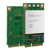
Telit Wireless Solutions LE910C1-AP Hardware Design Manual (79 pages)
mPCIe Cellular Module
Brand:
Telit Wireless Solutions
| Category:
Control Unit
| Size: 2 MB
Table of Contents
Notice
2
Copyrights
2
Computer Software Copyrights
2
Usage and Disclosure Restrictions
3
Applicability Table
4
Contents
5
Table of Contents
5
1 Introduction
10
Scope
10
Audience
10
Contact Information, Support
10
Text Conventions
11
Related Documents
12
2 General Product Description
13
Overview
13
Product Variants and Frequency Bands
14
Target Market
14
Table 1 Product Variants and Frequency Bands
14
Main Features
15
Table 2 Main Features
16
TX Output Power
17
RX Sensitivity
17
Table 3 Tx Output Power
17
Table 4 Rx Sensitivity
17
Mechanical Specifications
18
Dimensions
18
Weight
18
Temperature Range
19
Table 5 Temperature Range
19
3 Pins Allocation
20
Pin-Out
20
Table 6 Pin-Out
24
4 Power Supply
25
Power Supply Requirements
25
Power Consumption
25
Table 7 Power Supply Requirements
25
General Design Rules
26
Electrical Design Guidelines
26
Source Power Supply Design Guidelines
26
Figure 1 Linear Regulator with 5V Input
26
Source Power Supply Design Guidelines
27
Figure 2 Switching Regulator 12V
27
Battery Source Power Supply Design Guidelines
28
Thermal Design Guidelines
29
Power Supply PCB Layout Guidelines
30
Figure 3 Power Supply Recommended Circuit
31
Table 8 Vaux/Pwrmon Power Output
32
VAUX/PWRMON Power Output
32
Gnss Lna Bias
33
Table 9 Gnss Lna Bias
33
5 Electrical Specification
34
Absolute Maximum Ratings - Not Operational
34
Recommended Operating Conditions
34
Table 10 Absolute Maximum Ratings - Not Operational
34
Table 11 Recommended Operating Conditions
34
6 Digital Section
35
Logic Levels
35
Table 12 Absolute Maximum Rating Cmos 1.8V
35
Table 13 Absolute Maximum Rating Cmos 3.3V
35
Table 13 Operating Range Cmos 1.8V
36
Table 14 Operating Range Cmos 3.3V
36
Table 15 Operating Range Sim Card Pads
37
Power on
38
Figure 4 Power on Timing Diagramm
38
Unconditional Restart
41
Figure 5 Recomended Reset Driver Cuircuit
42
Power off Procedure
44
Figure 6 Shutdown by Software Command
44
Control Signals
46
Wake_N
46
Table 16 Perst_N
46
Table 17 Control Signals
46
Figure 7 Wake_N Internal Driver
47
W_Disable_N
48
Led_Wwan_N
48
Figure 8 Led_Wwan_N Internal Driver
48
Perst_N
49
Table 18 Perst_N Operating Levels
49
Hardware Interfaces
50
USB Port
50
Table 19 Hardware Interfaces
50
Table 20 Usb Interface
51
Serial Port
52
Modem Serial Port 1 Signals
52
Table 21 Modem Serial Port 1 Signals
52
RS232 Level Translation
53
Figure 9 Level Adapter Example
54
Figure 10 Rs232 Db-9 Pinout
54
I2C - Inter-Integrated Circuit
55
Digital Audio
55
Table 22 Digital Audio Interface
55
Figure 11 Sim Interface
57
SIM Interface
57
Table 23 Sim Interface Signals
57
7 Rf Section
58
Bands Variants
58
TX and RX Characteristics
58
Antenna Requirements
58
Antenna Connectors
58
Figure 12 Ufl Antenna Connectors
58
Main GSM/WCDMA/LTE Antenna Requirements
59
Table 24 Main Antenna Requirements
59
Antenna Diversity Requirements
60
GNSS Antenna Requirements
60
Table 25 Diversity Antenna Requirements
60
Combined GNSS Antenna
61
Linear and Patch GNSS Antenna
61
8 Mechanical Design
62
Mechanical Dimensions
62
Mechanical Drawing
62
Top View
62
Figure 13 Le910C1-Mpcie Top View (Dimensions Are in MM)
62
Bottom View
63
Figure 14 Le910C1-Mpcie Bottom View
63
Side View
64
Figure 15 Le910C1-Mpcie Side View
64
9 Application Pcb Design
65
Recommended Footprint for the Application
65
Figure 16 Le910C1-Mpcie Footprint Reference
65
10 Emc Recommendations
66
Table 26 Emc Recommendations
66
11 Packing System
67
Tray
67
Table 27 Tray Packing
67
Table 28 Packing Quantities
67
Figure 17 Le910C1-Mpcie Tray Organization
68
Tray Drawing
69
Figure 18 Le910C1-Mpcie Tray Drawing
69
Moisture Sensitivity
70
12 Conformity Assessment Issues
71
Declaration of Conformity
71
13 Safety Recommendations
72
Read Carefully
72
14 Reference Table of Rf Bands Characteristics
73
Table 29 Reference Table of Rf Bands
75
15 Acronyms
76
Table 30 Acronyms
77
16 Document History
78
Table 31 Document History
78
Telit Wireless Solutions LE910C1-AP Hw Design Manual (73 pages)
mPCIe
Brand:
Telit Wireless Solutions
| Category:
PCI Card
| Size: 1 MB
Table of Contents
Applicability Table
2
Table of Contents
3
Contents
3
1 Introduction
7
Scope
7
Audience
7
Contact Information, Support
7
Symbol Conventions
8
Related Documents
8
2 General Product Description
9
Overview
9
Product Variants and Frequency Bands
9
Target Market
10
Main Features
10
TX Output Power
11
RX Sensitivity
11
Mechanical Specifications
13
Dimensions
13
Weight
13
Temperature Range
13
3 Pins Allocation
14
Pin-Out
14
Pin-Out for the Full Compatibility with PCI Express Minicard Specification
16
4 Power Supply
20
Power Supply Requirements
20
Power Consumption
20
General Design Rules
20
Electrical Design Guidelines
21
Source Power Supply Design Guidelines
21
Source Power Supply Design Guidelines
22
Thermal Design Guidelines
23
Power Supply PCB Layout Guidelines
24
VAUX Power Output
26
Gnss Lna Bias
26
5 Electrical Specification
28
Absolute Maximum Ratings - Not Operational
28
Recommended Operating Conditions
28
6 Digital Section
29
Logic Levels
29
Power on
30
Unconditional Restart
32
Power off Procedure
35
Control Signals
36
Wake_N
37
W_Disable_N
38
Led_Wwan_N
38
Perst_N
39
Hardware Interfaces
40
USB Port
40
Serial Port
41
Modem Serial Port 1 Signals
42
RS232 Level Translation
42
I2C - Inter-Integrated Circuit
44
Digital Audio
44
SIM Interface
45
7 Rf Section
47
Band Variants
47
TX and RX Characteristics
47
Antenna Requirements
47
Antenna Connectors
47
Main GSM/WCDMA/LTE Antenna Requirements
48
Antenna Diversity Requirements
48
GNSS Antenna Requirements
49
Combined GNSS Antenna
50
Linear and Patch GNSS Antenna
50
8 Mechanical Design
51
Mechanical Dimensions
51
Mechanical Drawing (with SIM Holder)
51
Top View
51
Bottom View
53
Side View
54
Mechanical Drawing (Without SIM Holder)
55
Top View
55
Bottom View
56
Side View
57
9 Application Pcb Design
58
Recommended Footprint for the Application
58
10 Emc Recommendations
59
11 Packaging
60
Tray
60
Tray Packing
60
Packing Quantities
60
Tray Drawing
62
Moisture Sensitivity
63
12 Conformity Assessment Issues
64
Declaration of Conformity
64
13 Reference Table of Rf Bands Characteristics
65
14 Product and Safety Information
67
Copyrights and Other Notices
67
Copyrights
67
Computer Software Copyrights
67
Usage and Disclosure Restrictions
68
License Agreements
68
Copyrighted Materials
68
High Risk Materials
68
Trademarks
69
3Rd Party Rights
69
Waiwer of Liability
69
Safety Recommendations
70
15 Glossary
71
16 Document History
72
Telit Wireless Solutions LE910C1-AP Thermal Design Manual (26 pages)
Brand:
Telit Wireless Solutions
| Category:
Control Unit
| Size: 0 MB
Table of Contents
Applicability Table
2
Table of Contents
3
Contents
3
Introduction
5
Thermal Model
6
Temperature Sensor and Hotspot
6
Temperature Reading and Monitoring
7
Thermal Mitigation Algorithm
8
How to Change Thermal Mitigation Level Range
9
Thermal Model
13
Temperature Range
14
Current Consumption in each Mode
14
Thermal Design
16
Thermal Design Guidelines
16
Thermal Design Solution
17
Product and Safety Information
20
Copyrights and Other Notices
20
Copyrights
20
Computer Software Copyrights
20
Usage and Disclosure Restrictions
21
License Agreements
21
Copyrighted Materials
21
High Risk Materials
21
Trademarks
22
Third Party Rights
22
Waiwer of Liability
22
Safety Recommendations
23
Advertisement
Related Products
Telit Wireless Solutions LE910C1-APX
Telit Wireless Solutions LE910C1-NS
Telit LE910C1-EU
Telit Wireless Solutions LE910C1-NA
Telit Wireless Solutions LE910C1 Series
Telit Wireless Solutions LE910C1C1
Telit Wireless Solutions LE910C1-NAD
Telit Wireless Solutions LE910C1-NFD
Telit Wireless Solutions LE910C1-SAD
Telit Wireless Solutions LE910C1-SAXD
Telit Wireless Solutions Categories
Control Unit
Wireless modules
Motherboard
Computer Hardware
Microcontrollers
More Telit Wireless Solutions Manuals
Login
Sign In
OR
Sign in with Facebook
Sign in with Google
Upload manual
Upload from disk
Upload from URL