Table of Contents
Advertisement
Quick Links
Advertisement
Table of Contents

Related Manuals for HighPoint HPT366


Summary of Contents for HighPoint HPT366
- Page 1 OINT ECHNOLOGIES,INC. www.highpoint-tech.com...
- Page 2 The products described in this publication are products of HighPoint Technologies. Copyright 1999 By HighPoint Technologies, Inc. All Rights Reserved Printed in U.S.A.
- Page 3 HighPoint Technologies,Inc Preface Preface This manual assumes some prior knowledge of current and information of HPT366 Standard. The data manual organized into the following chapter : Chapter 1- Overview, Chapter 2- Signal Description, Chapter 3- Registers. Chapter 4- Electrical Parameters, Chapter 5- Timing, Appendix A- Mechanical Dimensions.
-
Page 4: Table Of Contents
HighPoint Technologies,Inc Contents Table of Contents Chapter 1 Overview Introduction ........................... 1-1 1.1 HPT366 Block Diagram ......................1-2 1.2 Features ..........................1-3 Chapter 2 Signal Description Introduction Pins ..........................2-1 2.1 144 Pins Signal Description ...................... 2-2 2.2 144 Pins Listing ........................2-3 System Pins .......................... - Page 5 DC Specifications ........................4-2 AC Specifications ........................4-3 Chapter 5 Timing Introduction ............................. 5-1 5.1 Timing Parameters ........................5-2 5.2 Clock Timing ..........................5-3 5.3 Read Transaction ........................5-4 5.4 Write Transaction ........................5-5 5.5 IDE Timing ........................5-6,5-7,5-8 HPT366 Data Manual www.highpoint-tech.com...
- Page 6 A.1 144 Pins LQFP ........................A-2 Appendix B Diagrams Introduction ............................ B-1 B.1 Schematic Diagrams For Add-On Card ..................B-2 B.2 Layout For Add-On Card ......................B-3 B.3 Schematic Diagrams For Main Board ................B-4,B-5 HPT366 Data Manual iiii www.highpoint-tech.com...
-
Page 7: Overview
HighPoint Technologies,Inc Overview/Introduction Chapter 1 Overview Introduction This chapter will combines information and features for the HPT366. HPT366 has been designed to let you add additional high performance device(s) to your current computer system. HPT366 Data Manual www.highpoint-tech.com... - Page 8 1.1 Block Diagram Decoder Primary Timing Master Control1 PCI IF FIFO IDE IF Timing Primary Control2 Slave Decoder Secondary Timing Master Control1 FIFO PCI IF IDE IF Timing Secondary Control2 Slave PROM Serial EPROM Parallel EPROM HPT366 Data Manual www.highpoint-tech.com...
-
Page 9: Features
(Loading address 0 for serial size EPROM, loading address 400H for parallel EPROM.) • 144 Pin LQFP(Dedicated Parallel EPROM pins). • Small foot print 144 pin LQFP • Up to 44MHz PCI bus Clock. • Multifunction • Embeded serial resistor on chip for ATA spec. HPT366 Data Manual www.highpoint-tech.com... -
Page 10: Signal Description
* PCI Interrupt Pins, * Address/Data Pins, * IDE Interface Pins, * EPROM Interface Pins, * Other Pins. There are three signal type definitions: Input, a standard input-only signal. Totem Pole Output, a standard output driver. Input and Output. HPT366 Data Manual www.highpoint-tech.com... - Page 11 PIOW_ gndado PIOR_ HPT366 PIORDY SD6/MD6 PDACK_ 144 Pins IRQ14 PA1/MA14 SD7/MD7 PCBLID/MA16 PA0/MA13 SRST_ PA2/EFMCS_ SDA/EFM_WE_ PCS0_/MA0 SCL/EFM_OE_ PCS1_/MA1 INTA_ INTB_ PCIRST_ gndado PCICLK gndado GNT_ PCIREQ_ AD31 AD30 gndado AD29 AD28 C_BE_0 Pin 1 HPT366 Data Manual www.highpoint-tech.com...
-
Page 12: 144 Pins Listing
Ground reference power supply IC, input and output. 90,91,92 VSSI Ground reference power supply onput, input and IC. 1,25,35, Positive power supply output. 98,121,144 72,73 VDDI Positive power supply output and IC. 13,40,46, gndado Ground Output 71,123,137 HPT366 Data Manual www.highpoint-tech.com... -
Page 13: Interface Control Pins
Pin Number Pin Name Type Description PCIREQ_ Request indicates to the system arbiter that this agent desires use of the PCI bus. GNT_ Grant indicates to the agent that access to the PCI bus has been granted. HPT366 Data Manual www.highpoint-tech.com... -
Page 14: Pci Interrupt Pins
C_BE_3 to byte 3. Parity is the even parity bit that protects the AD(31-0) and C_BE_(3-0) lines. During address phase, both the address and command bits are covered. During data phase, both data and byte enables are covered. HPT366 Data Manual www.highpoint-tech.com... -
Page 15: Ide Interface Pins
Primary IDE Channel I/O Ready SDRQ Secondary IDE DMA Request PDRQ Primary IDE DMA Request 61,63,65,67, PD(15-0) Primary IDE Data 69,74,76,78, 79,77,75,70, 68,66,64,62 51,54,52 PA(2-0) Primary IDE Device Address Them are also used as EFMCS_ and Memory Address Bus signal. HPT366 Data Manual www.highpoint-tech.com... -
Page 16: Eprom Interface Pins
SDA/EFM_WE_ & TRI signals are both high-LEV, the configuration will be loaded from parallel EPROM automatically. It is also used as a SDA signal. PA2/ EPROM Chip Select. It is also used as a Primary IDE Device EFMCS_ Address signal. HPT366 Data Manual www.highpoint-tech.com... -
Page 17: Other Pins
When system reset, the MA7 signal will be latched on rising edge of PCIRST_ signal. If the value is 1, the IC is packaged of 144 Pins. The MA7 pin must have a external pull_up resistor (<5K). HPT366 Data Manual www.highpoint-tech.com... -
Page 18: Registers
This chapter will introduction PCI Configuration Registers and I/O Space Registers. HPT366 have two functions. In this chapter, there just list the registers of most same as PCI function 0, expect a few registers which have been listed at the same location. -
Page 19: Registers Listing
Header Type Register Command Block Register Registers Control Block Register I/O Space Base Register CardBus CIS Pointer Register Subsystem Vendor ID Register Subsystem ID Register Expansion ROM Base Register 3-10 Interrupt Line Register 3-10 Interrupt Pin Register HPT366 Data Manual www.highpoint-tech.com... - Page 20 3-15 MISC.Control4 Register Bus Status1 Register 3-16 Bus Status2 Register 3-17 Cable Select Register 3-17 Bus Master Command Register 3-18 I/O Space Registers Bus Master Status Register 3-18 Bus Master Scatter Gather Table Base Register 3-19 HPT366 Data Manual www.highpoint-tech.com...
-
Page 21: Pci Configuration Registers
These fields identify the manufacturer of the device and particular device. Command Register Address: 04h-05h Attribute: R/W DESCRIPTION 15:10 Reserved Fast Back-to-Back Enable(Not Implemented).Hardwired 0 8 : 3 Reserved Bus Master Enable.If set 1,Master Mode Enable. Memory Space Enable.1=Enable.0=Disable. I/O Space Enable.1=Enable.0=Disable. HPT366 Data Manual www.highpoint-tech.com... -
Page 22: Status Register
DEVSEL_ Timing.Hardwired 01-Medium. Reserved *Notes: Reads to this register behave normally. Revision Identification Register Address: 08h Attribute: Read Only/Power On Loading DESCRIPTION 7 : 0 Revision ID Byte=01h. *Note: This field specifies device and revision identifiers. HPT366 Data Manual www.highpoint-tech.com... -
Page 23: Class Code Register
Latency Timer Register Address:0Dh Attribute: R/W DESCRIPTION 7 : 0 Latency Timer *Notes: The Latency Timer Register specifies, in units of PCI bus clocks, the value of the Latency Timer for this PCI bus master. HPT366 Data Manual www.highpoint-tech.com... -
Page 24: Header Type Register
*Notes: In mode the registers of the IDE channels are completely relocatable in I/O space. Base Address sters in the PCI IDE controller Configuration Space registers are used to map the IDE register into pace. HPT366 Data Manual www.highpoint-tech.com... -
Page 25: Control Block Register
I/O Space Base Register Address: 20h-23h Attribute: R/W DESCRIPTION 31:8 I/O Base Address. Reserved. Hardwired to 1. CardBus CIS Pointer Register Address: 28h Attribute: Read Only. Power On Loading Description 31:0 CardBus CIS Pointer. HPT366 Data Manual www.highpoint-tech.com... -
Page 26: Subsystem Vendor Id Register
ROM. When the bit is set, address decoding is enabled, and a device is used with or without an expansion ROM depending on the system configuratio. To access the external memory interface, also set the Memory Space bit in the Command register. It exists in function 0 only! HPT366 Data Manual www.highpoint-tech.com... -
Page 27: Interrupt Line Register
In the function 2, Hardwired to 2. Connected to INTB_. *Notes: This register tells which interrupt pin the device uses. Its value is set to 01h for the Function A INTA_ signal, and 02h for the Function B INTB_ signal at power-up. HPT366 Data Manual 3-10 www.highpoint-tech.com... -
Page 28: Ide Timing0 Register
Primary Drive 0 cmd_pre_high_time. 21:19 Primary Drive 0 pre_high_time. 18:16 Primary Drive 0 udma_cycle_time. 15:12 Primary Drive 0 cmd_low_time. 11:8 Primary Drive 0 cmd_high_time. Primary Drive 0 low time cycle number. Primary Drive 0 high time cycle number. HPT366 Data Manual 3-11 www.highpoint-tech.com... -
Page 29: Ide Timing1 Register
Primary Drive 1 cmd_pre_high_time. 21:19 Primary Drive 1 pre_high_time. 18:16 Primary Drive 1 udma_cycle_time. 15:12 Primary Drive 1 cmd_low_time. 11:8 Primary Drive 1 cmd_high_time. Primary Drive 1 low time cycle number. Primary Drive 1 high time cycle number. HPT366 Data Manual 3-12 www.highpoint-tech.com... -
Page 30: Misc.control1 Register
IDE Device Registers are allocated to I/O. BA OFFSET 0X10, 0X14. This Bit =0 (Disable) means all Primary IDE Registers are at Default IDE Address. This bit is Read Only. (Note: In Function second, it's adress is 170-177 and 376.) HPT366 Data Manual 3-13 www.highpoint-tech.com... -
Page 31: Misc.control2 Register
State Machine by Writing a 1 to this bit. Clear Master State Machine is one PCI Clock Pulse. Clear SG Counter bit. 0=Not Clear Counter. 1=Clear Counter. Software Clear SG Counter by Writing a 1 to this bit. Clear SG Counter is one PCI Clock Pulse. HPT366 Data Manual 3-14 www.highpoint-tech.com... -
Page 32: Misc.control3 Register
0 to disable pseudo-dma. After reset,this bit is set to 0. R/W Bus Parking AD&CBE output enable. 1=enable, 0=disable. If this bit enable when PCI GNT_ Parking on IDE,PCI AD&CBE will be drive by HPT366. After Reset this bit=0. R/W 29-27 SG State Machine Number. -
Page 33: Bus Status1 Register
Attribute: Bit 0-5 is Read Only; Bit 6-7 is R/W. DESCRIPTION Secondary channel POLL_INT_EN Primary channel Auto POLL Interrupt Enable. If this bit is "1", HPT366 hardware will generate an interrupt upon a successful auto Poll. (R/W) Secondary channel DMARQ. -
Page 34: Bus Status2 Register
Secondary IRQ_DEV1. R Secondary channel IRQ_DEV0. R Primary Auto POLL Function Enable. If this bit is set, HPT366 will start auto poll function after an NOP Auto Poll command is issued by the host. As defined by ATA/ATAPI-4 specification, HPT366 will return ERR bit as "0"... -
Page 35: I/O Space Registers
Bus Master R/W Control.Bus Master Read (Disk Write)=0,Bus Master Write (DiskRead)=1. Reserved Start/Stop Bit.Start=1, Stop=0.When This Bit is set to 1, Bus Master operat- ion will be started. After this Bit is clear to 0,Bus Master operation will be stopped. HPT366 Data Manual 3-18 www.highpoint-tech.com... -
Page 36: Bus Master Status Register
Read Only Bit. Bus Master Active Bit. 1=Bus master operation is processing. 0=no bus master operation. Bus Master Scatter Gather Table Base Register Primary Channel: 04h-07h Secondary Channel: 0Ch-0Fh Attribute: R/W DESCRIPTION 31:2 Bus Master Scatter Gather Table Base Address. 1 : 0 Reserved HPT366 Data Manual 3-19 www.highpoint-tech.com... -
Page 37: Electrical Parameters
Electrical Parameters/Introduction Chapter 4 Electrical Parameters Introduction This chapter defines all the electrical characteristics and constraints of PCI components, systems. The PCI electrical definition provides for 3.3V signaling environments, and all IOs of HPT366 are 5V tolerant. HPT366 Data Manual www.highpoint-tech.com... -
Page 38: Signaling Environment
3. Lower capacitance on this input-only pin allows for non-resistive coupling to AD[xx]. 4. This is a recommendation, not an absolute requirement. The actual value should be provided with the component data sheet. HPT366 Data Manual www.highpoint-tech.com... -
Page 39: Ac Specifications
The equation defined maxima should be met by design. 3. This parameter is to be interpreted as the cumulative edge rate across the specified range, rather than the instantaneous rate at any point within the transition range. HPT366 Data Manual www.highpoint-tech.com... -
Page 40: Timing
HighPoint Technologies,Inc Timing/Introduction Chapter 5 Timing Introduction This chapter is organized into the following sections: Timing Parameters Clock Timing Read Transaction Write Transaction IDE Timing HPT366 Data Manual www.highpoint-tech.com... -
Page 41: Timing Parameters
10; REQ has a setup of 12. All other signals are bused. 3. RST_ is asserted and deasserted asynchronously with respect to CLK. 4. All output drivers must be asynchronously floated when RST_ is active. HPT366 Data Manual www.highpoint-tech.com... -
Page 42: Clock Timing
The clock may only be stopped in a low state. 2. The minium clock period must not be violated for any single clock cycle, i.e., accounting for all system jitter. HPT366 Data Manual www.highpoint-tech.com... -
Page 43: Read Transaction
The transaction starts with an address phase which occurs when FRAME_ is asserted for the first time and occurs on clock2. During the address pha- se, AD[31:0] contain a valid address and C_BE_[3:0] contain a valid bus command. HPT366 Data Manual www.highpoint-tech.com... -
Page 44: Write Transaction
2. A write transaction is similar to a read transaction ex- cept no turnaround cycle is required following the address phase becau- se the master provides both address and data. Data phases work the sa- me for both read and write transactions. HPT366 Data Manual www.highpoint-tech.com... -
Page 45: Ide Timing
3. The negation of IORDY_ by the device is used to extend the PIO cycle. The determination of whether the cycle is to be extended is made by the host after A from the assertion of DIOR-or DIOW-. HPT366 Data Manual www.highpoint-tech.com... - Page 46 DIOR-/DIOW- to address valid hold (min) Read Data Valid to IORDY active(if IORDY initially low after tA) (min) IORDY Setup time (min) IORDY Pulse Width (max) 1250 1250 1250 1250 1250 IORDY assertion to release (max) HPT366 Data Manual www.highpoint-tech.com...
- Page 47 If the device is driving IORDY# ne- gated at the time t after the activation of DIOR- or DIOW-, then RD shall be met and t is not applicable. HPT366 Data Manual www.highpoint-tech.com...
-
Page 48: Mechanical Dimensions
HighPoint Technologies,Inc Mechanical Dimensions Appendix A Mechanical Dimensions This chapter contains the package drawing for the HPT366. One configuration is available, a 144 Pins LQFP. HPT366 Data Manual www.highpoint-tech.com... -
Page 49: 144 Pins Lqfp
HighPoint Technologies,Inc Mechanical Dimensions/144 Pins LQFP A.2 144 Pins LQFP HPT366 Data Manual www.highpoint-tech.com... -
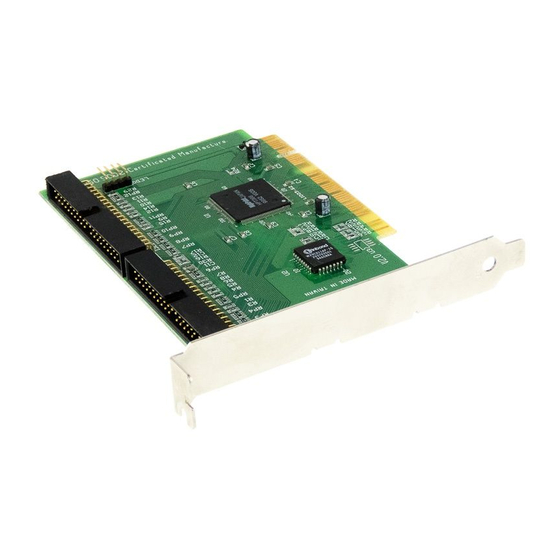
Page 50: Diagrams Introduction
HighPoint Technologies,Inc Diagrams/Introduction Appendix B Diagrams Introduction This appendix contains the following items: * Schematic Diagrams For Add-On Card; * Layout For Add-On Card; * Schematic Diagrams For Main Board. HPT366 Data Manual www.highpoint-tech.com... - Page 51 HighPoint Technologies,Inc Diagrams/Schematic Diagrams For Add-On Card B.1 Schematic Diagrams HPT366 Data Manual www.highpoint-tech.com...
- Page 52 HighPoint Technologies,Inc Diagrams/Layout For Add-On Card B.2 Layout Top Layer HPT366 Data Manual www.highpoint-tech.com...
-
Page 53: Schematic Diagrams For Main Board
HighPoint Technologies,Inc Diagrams/Schematic Diagrams For Main Board B.3 Schematic Diagrams For Main Board HPT366 Data Manual www.highpoint-tech.com... - Page 54 3. Connecting TRI pin(Pin 81) to low will float the ATA Bus. This feature can be used for hotswap application. 4. HPT366’s power supply is 3.3v. The option box on the lower right corner on the schematics may be used for system with 5v supply.
Need help?
Do you have a question about the HPT366 and is the answer not in the manual?
Questions and answers