Table of Contents
Advertisement
Quick Links
www.ti.com
User's Guide
OPA928 Evaluation Module
This user's guide describes the operation and use of the OPA928 evaluation module (EVM). The user's guide
provides information on how to set up the EVM and describes different circuit configurations that can be used to
evaluate the performance of the
the terms evaluation board, evaluation module, and EVM are synonymous with the OPA928EVM. This document
also includes an electrical schematic, simplified schematics of OPA928 applications circuits, a printed circuit
board (PCB) layout drawing, and a parts list for the EVM.
For best possible performance, make sure to review the
SBOU282A – DECEMBER 2022 – REVISED MARCH 2023
Submit Document Feedback
ABSTRACT
OPA928
femtoampere, input-bias-current op amp. Throughout this document,
Note
Copyright © 2023 Texas Instruments Incorporated
Section 1.1
before handling the EVM board.
OPA928 Evaluation Module
1
Advertisement
Table of Contents

Related Manuals for Texas Instruments OPA928


Summary of Contents for Texas Instruments OPA928
- Page 1 OPA928 Evaluation Module ABSTRACT This user’s guide describes the operation and use of the OPA928 evaluation module (EVM). The user's guide provides information on how to set up the EVM and describes different circuit configurations that can be used to...
-
Page 2: Table Of Contents
1 Read This First..................................3 1.1 EVM Cleanliness Guidelines..............................3 Overview....................................4 2.1 Guarding and Shielding..............................4 3 Getting Started..................................5 3.1 Related Documentation From Texas Instruments......................3.2 Electrostatic Discharge Caution............................4 EVM Circuit Description.................................6 4.1 High-Impedance Amplifier Circuit............................6 4.2 Transimpedance Amplifier Circuit............................5 Cleaning the EVM..................................13 5.1 Ultrasonic Wash................................ -
Page 3: Read This First
The EVM must be cleaned per these instructions anytime the board is soldered or modified near sensitive nodes, or if these nodes become contaminated by other means. SBOU282A – DECEMBER 2022 – REVISED MARCH 2023 OPA928 Evaluation Module Submit Document Feedback Copyright © 2023 Texas Instruments Incorporated... -
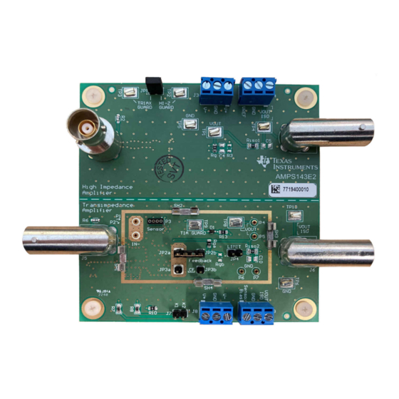
Page 4: Overview
The two OPA928 amplifiers, U1 and U2, are located on the bottom side of the EVM and are enclosed within grounded RF shields to protect from contamination, noise, and electromagnetic interference (EMI). The top side of the EVM features a variety of pin sockets, jumpers, and other components that provide easy configuration, while limiting the potential for performance-degrading contamination at sensitive nodes. -
Page 5: Getting Started
TIA circuit has an additional terminal block (J7) requiring two independently-controlled 5-V channels to drive a T-switch that discharges the feedback loop (see Section 4.2.2.1). The EVM can be used without this function, in which case J7 can be ignored. 3.1 Related Documentation From Texas Instruments Document Literature Number OPA928 product data sheet SBOSA77 3.2 Electrostatic Discharge Caution... -
Page 6: Evm Circuit Description
The guard buffer tracks the potential of the amplifier input as the common-mode input voltage changes. The guard pin of the OPA928 can be connected to the triax cable guard by installing a shunt jumper at JP1. If the guard of the triax connector is not driven by another source, install the jumper at JP1. The amplifier and input traces are located on the bottom of the PCB and are fully enclosed by a grounded RF shield to prevent noise and EMI from coupling into the signal path. -
Page 7: Transimpedance Amplifier Circuit
The input path consists of BNC connector (J5) and 0-Ω series resistor (R4) connected to the inverting input of the OPA928 (U2). The inverting input can be accessed directly through pin sockets P1 and P2. -
Page 8: Table 4-1. Tia Jumper Block Connections
Table 4-2. TIA Pin Socket Configurations Designator Node P1, P2 Inverting Input (U2) Sensor Bias (J9) P4, P5 Vout (U2) P6, P7 Analog Ground (GND) OPA928 Evaluation Module SBOU282A – DECEMBER 2022 – REVISED MARCH 2023 Submit Document Feedback Copyright © 2023 Texas Instruments Incorporated... -
Page 9: Figure 4-3. T-Switch Timing Diagram
When the pins of J7 are not actively driven, the control logic is pulled to ground by R11 and R12, resulting in a default logic low for normal TIA operation. SBOU282A – DECEMBER 2022 – REVISED MARCH 2023 OPA928 Evaluation Module Submit Document Feedback Copyright © 2023 Texas Instruments Incorporated... -
Page 10: Figure 4-4. T-Switch Logic Low (Normal Operation)
T-switch circuit when the logic is driven high and the feedback is discharged. K1 opens and K2 closes, switching 10-kΩ resistor R5 into the feedback parallel to CF. This 10-kΩ resistor provides OPA928 Evaluation Module SBOU282A – DECEMBER 2022 – REVISED MARCH 2023 Submit Document Feedback Copyright © 2023 Texas Instruments Incorporated... -
Page 11: Figure 4-6. T-Switch Logic High (Discharge Feedback)
C9, is populated in parallel to R5 to maintain stability when the T-switch is active. 10 k 100 pF – Riso2 OPA928 Sensor ¡ Bias Figure 4-7. T-Switch Logic High Equivalent Circuit (Discharge Feedback) SBOU282A – DECEMBER 2022 – REVISED MARCH 2023 OPA928 Evaluation Module Submit Document Feedback Copyright © 2023 Texas Instruments Incorporated... -
Page 12: Figure 4-8. Guarded Diode Limiter
Instead, the circuit shown in Figure 4-8 takes advantage of the OPA928 internal guard buffer and the internal ESD protection to implement a guarded diode limiter. The internal guard buffer maintains the input common-mode potential on both sides of the internal ESD diodes. -
Page 13: Cleaning The Evm
6 Schematic, PCB Layout, and Bill of Materials This section provides the OPA928EVM hardware schematics, PCB layout and bill of materials. SBOU282A – DECEMBER 2022 – REVISED MARCH 2023 OPA928 Evaluation Module Submit Document Feedback Copyright © 2023 Texas Instruments Incorporated... -
Page 14: Evm Schematic
GND HI-Z 5016 5016 OSTTE030161 3.3pF GUARD HI-Z 5016 Rgnd GND HI-Z GND TIA GND HI-Z Figure 6-1. OPA928EVM Hi-Z Schematic OPA928 Evaluation Module SBOU282A – DECEMBER 2022 – REVISED MARCH 2023 Submit Document Feedback Copyright © 2023 Texas Instruments Incorporated... -
Page 15: Figure 6-2. Opa928Evm Tia Schematic
GND TIA DGND GND TIA GND TIA S1711-46R 100k 100k S1711-46R DGND S1711-46R DGND GND TIA Figure 6-2. OPA928EVM TIA Schematic SBOU282A – DECEMBER 2022 – REVISED MARCH 2023 OPA928 Evaluation Module Submit Document Feedback Copyright © 2023 Texas Instruments Incorporated... -
Page 16: Pcb Layout
The top and bottom solder mask layers are included to show where the solder mask was removed from guard copper and RF shield mount areas. Figure 6-3. Top Overlay Figure 6-4. Top Solder Mask OPA928 Evaluation Module SBOU282A – DECEMBER 2022 – REVISED MARCH 2023 Submit Document Feedback Copyright © 2023 Texas Instruments Incorporated... -
Page 17: Figure 6-5. Top Layer Pcb Layout
Schematic, PCB Layout, and Bill of Materials Figure 6-5. Top Layer PCB Layout Figure 6-6. Internal Power Layer PCB Layout SBOU282A – DECEMBER 2022 – REVISED MARCH 2023 OPA928 Evaluation Module Submit Document Feedback Copyright © 2023 Texas Instruments Incorporated... -
Page 18: Figure 6-7. Internal Guard Layer Pcb Layout
Schematic, PCB Layout, and Bill of Materials www.ti.com Figure 6-7. Internal Guard Layer PCB Layout Figure 6-8. Bottom Layer PCB Layout OPA928 Evaluation Module SBOU282A – DECEMBER 2022 – REVISED MARCH 2023 Submit Document Feedback Copyright © 2023 Texas Instruments Incorporated... -
Page 19: Figure 6-9. Bottom Solder Mask
Schematic, PCB Layout, and Bill of Materials Figure 6-9. Bottom Solder Mask Figure 6-10. Bottom Overlay SBOU282A – DECEMBER 2022 – REVISED MARCH 2023 OPA928 Evaluation Module Submit Document Feedback Copyright © 2023 Texas Instruments Incorporated... -
Page 20: Bill Of Materials
1.0 x 2.0 x 0.75 Fotofab MP2, MP3 Standard RF Shield 1.0 x 1.5 x 0.25 RF_SHIELD 1.0 x 1.5 x 0.25 Fotofab OPA928 Evaluation Module SBOU282A – DECEMBER 2022 – REVISED MARCH 2023 Submit Document Feedback Copyright © 2023 Texas Instruments Incorporated... - Page 21 4 (1 x 4) Position Shunt Connector Black JUMPER 69144-204LF Amphenol ICC Open Top 0.100" (2.54mm) Gold or Gold, GXT™ SBOU282A – DECEMBER 2022 – REVISED MARCH 2023 OPA928 Evaluation Module Submit Document Feedback Copyright © 2023 Texas Instruments Incorporated...
- Page 22 Amplifier, SOIC8 0805 C5, C10 0805 FID1, FID2, Fiducial mark. There is nothing to buy or FID3 mount. R3, Rgb 0805 OPA928 Evaluation Module SBOU282A – DECEMBER 2022 – REVISED MARCH 2023 Submit Document Feedback Copyright © 2023 Texas Instruments Incorporated...
- Page 23 STANDARD TERMS FOR EVALUATION MODULES Delivery: TI delivers TI evaluation boards, kits, or modules, including any accompanying demonstration software, components, and/or documentation which may be provided together or separately (collectively, an “EVM” or “EVMs”) to the User (“User”) in accordance with the terms set forth herein.
- Page 24 www.ti.com Regulatory Notices: 3.1 United States 3.1.1 Notice applicable to EVMs not FCC-Approved: FCC NOTICE: This kit is designed to allow product developers to evaluate electronic components, circuitry, or software associated with the kit to determine whether to incorporate such items in a finished product and software developers to write software applications for use with the end product.
- Page 25 www.ti.com Concernant les EVMs avec antennes détachables Conformément à la réglementation d'Industrie Canada, le présent émetteur radio peut fonctionner avec une antenne d'un type et d'un gain maximal (ou inférieur) approuvé pour l'émetteur par Industrie Canada. Dans le but de réduire les risques de brouillage radioélectrique à...
- Page 26 www.ti.com EVM Use Restrictions and Warnings: 4.1 EVMS ARE NOT FOR USE IN FUNCTIONAL SAFETY AND/OR SAFETY CRITICAL EVALUATIONS, INCLUDING BUT NOT LIMITED TO EVALUATIONS OF LIFE SUPPORT APPLICATIONS. 4.2 User must read and apply the user guide and other available documentation provided by TI regarding the EVM prior to handling or using the EVM, including without limitation any warning or restriction notices.
- Page 27 Notwithstanding the foregoing, any judgment may be enforced in any United States or foreign court, and TI may seek injunctive relief in any United States or foreign court. Mailing Address: Texas Instruments, Post Office Box 655303, Dallas, Texas 75265 Copyright © 2023, Texas Instruments Incorporated...
- Page 28 TI products. TI’s provision of these resources does not expand or otherwise alter TI’s applicable warranties or warranty disclaimers for TI products. TI objects to and rejects any additional or different terms you may have proposed. IMPORTANT NOTICE Mailing Address: Texas Instruments, Post Office Box 655303, Dallas, Texas 75265 Copyright © 2023, Texas Instruments Incorporated...
Need help?
Do you have a question about the OPA928 and is the answer not in the manual?
Questions and answers