
Related Manuals for Aim AMCX-FDX-2


Summary of Contents for Aim AMCX-FDX-2
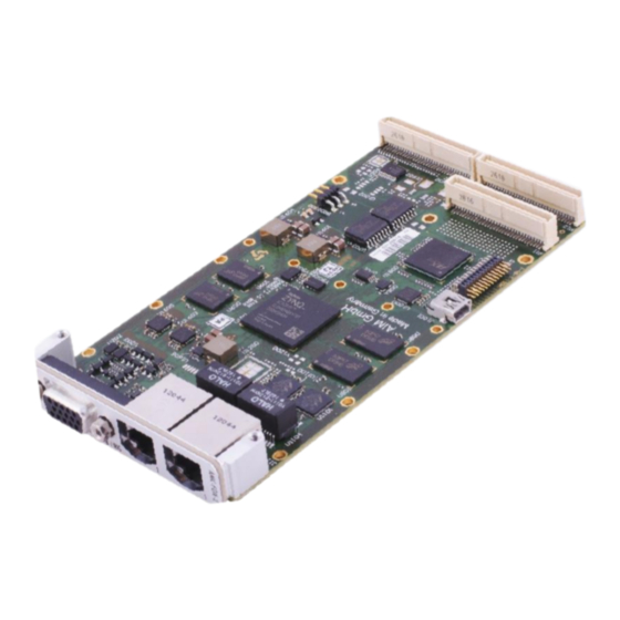
- Page 1 AMCX-FDX-2 10/100/1000Mbit AFDX / ARINC664 Test and Simulation PMC Interface Module Hardware Manual V01.00 Rev. A September 2017...
- Page 3 AMCX-FDX-2 10/100/1000Mbit AFDX/ARINC664 Test and Simulation PMC Interface Module Hardware Manual V01.00 Rev. A September 2017 AIM No. 60-15A30-16-0100-A AMCX-FDX-2 Hardware Manual...
- Page 4 Notice: The information that is provided in this document is believed to be accurate. No responsibility is assumed by AIM GmbH for its use. No license or rights are granted by implication in connection therewith. Specifications are subject to change without notice.
- Page 5 DOCUMENT HISTORY The following table defines the history of this document. Version Cover Date Created by Description 01.00 Rev A 13.09.2017 Marco Maier First Release AMCX-FDX-2 Hardware Manual...
- Page 6 THIS PAGE IS INTENTIONALLY LEFT BLANK AMCX-FDX-2 Hardware Manual...
-
Page 7: Table Of Contents
Connecting to Other Devices ....................4 2.3.1 AFDX Connection ........................5 2.3.2 Trigger, Discrete and IRIG Connector ..................5 2.3.3 AMCX-FDX-2 Rear I/O Interface ..................... 7 Structure of the AMCX-FDX-2 ................9 System on Chip (SoC) ......................11 3.1.1 Ethernet MAC Features ......................11 3.1.2 PCI-Express Bus and DMA Engine ..................11... - Page 8 LIST OF FIGURES Figure Title Page Figure 2-1: Installing the AMCX-FDX-2 on a PMC carrier module ........4 Figure 2-2: Front panel View of AMCX-FDX-2 ..............4 Figure 2-3: Pinout DSUB ....................5 Figure 3-1: AMCX-FDX-2 Block Diagram ..............10 Figure 3-2: GPI/O AMCX-FDX-2 circuitry ..............
-
Page 9: Introduction
'Applicable Documents' section. The AMCX-FDX-2 module is a member of AIM's family of advanced PMC-Bus modules for analysing, simulating, monitoring and testing of avionic Databus Systems. The AMCX-FDX-2 module is used to simulate, monitor and inject protocol errors of AFDX based network systems as well as common Ethernet networks with a data rate of 10/100/1000 Mbit/s. -
Page 10: How This Manual Is Organized
2 device, and connect the device to other external interfaces including the AFDX Network, IRIG-B, and triggers. Section 3 - Structure of the AMCX-FDX-2 - describes the physical hardware interfaces of the AMCX-FDX-2 using a block diagram and a description of... -
Page 11: Instalation
2 INSTALATION 2.1 Preparation and Precaution for Installation The AMCX-FDX-2 features full PMC Plug and Play capability, therefore, there are no jumpers or switches on the board that require modification by the user in order to interface to the PMC bus. -
Page 12: Connecting To Other Devices
PMC carrier module 2.3 Connecting to Other Devices The external interfaces of the AMCX-FDX-2 consist of two RJ45 Ethernet connectors, Trigger In/Out signal, Discrete IO signals, Ground as well as IRIG In/Out interface for multi-channel time tag synchronization. -
Page 13: Afdx Connection
2.3.2 Trigger, Discrete and IRIG Connector For multi-channel time tag synchronization an input for the on-board IRIG-Decoder and an output for inter-board synchronization is available. The output format is an AIM specific IRIG coded signal. The connector also provides four Trigger input/output signals, which can be used with dedicated applications. - Page 14 No connection required Multiple AIM-Modules with no common synchronization requirement No connection required Single or multiple AIM-Module(s) with external IRIG-B source Connect external IRIG-B source to IRIG-IN and GND of all modules Multiple AIM-Modules with no external IRIG-B source internally synchronized.
-
Page 15: Amcx-Fdx-2 Rear I/O Interface
2. Instalation 2.3.3 AMCX-FDX-2 Rear I/O Interface Instead of using the front panel interface, the P14 PMC Rear I/O connector can be used to access Trigger lines, Discrete I/O and the PXI Trigger Interface. PMC Connector P14 Signal Signal Reserved... - Page 16 2. Instalation THIS PAGE INTENTIONALLY LEFT BLANK AMCX-FDX-2 Hardware Manual...
-
Page 17: Structure Of The Amcx-Fdx-2
3. Structure of the AMCX-FDX-2 3 STRUCTURE OF THE AMCX-FDX-2 The structure of the AMCX-FDX-2 board is shown in the block diagram on the next page. The AMCX-FDX-2 comprises the following main sections: System on a Chip design with ... -
Page 18: Figure 3-1: Amcx-Fdx-2 Block Diagram
2 GB PS Dual- RX RAM Core (optional) NAND / QSPI Boot Flash PCIe Endpoint IRIG NOVRAM PCIe 2.0 x1 PCIe-to-PCI Quartz & Bridge Clock Buffer 32bit / 66MHz PCI Host PMC connector Figure 3-1: AMCX-FDX-2 Block Diagram AMCX-FDX-2 Hardware Manual... -
Page 19: System On Chip (Soc)
Receiver data from On-Board memory to Host memory. This is done fully independent from any processor interaction to ensure maximum performance. On the AMCX-FDX-2, this PCIe endpoint is used as a local bus, connected to a powerful PCIe-to-PCI Bridge for interfacing the Host PMC Interface. -
Page 20: Irig- And Time Code Section
3.1.3.2 Timecode Encoder/Decoder On the AMCX-FDX-2 a freewheeling IRIG function is implemented. If no external IRIG signal is detected, the IRIG Decoder switches automatically to the freewheeling operation mode. If an external IRIG-B signal is detected in freewheeling mode, the Time Tag is automatically synchronized to this external IRIG-B signal. -
Page 21: Application Specific Processor
Setup Receive and Transmit DMA machines in the PL Relieve the Host system, fasten up the board and expands the capability of the AMCX-FDX-2 module to a high level instrument. 3.1.5 BIU Processor Core 2 of the Dual Core Processor is used as Bus Interface Processor (BIP) and handles the real time critical control of the two AFDX ports. -
Page 22: Pcie-To-Pci Bridge
AMCX-FDX-2 3.3 PCIe-to-PCI Bridge The AMCX-FDX-2 interfaces to the Host with a 32bit PCI / PMC Interface running up to 66MHz. The PCIe-to-PCI Bridge has 3.3V and 5V tolerant I/O, and supports PCI Revision 3.0 protocols. PCI Power Management 1.1 is supported. -
Page 23: Figure 3-2: Gpi/O Amcx-Fdx-2 Circuitry
Discrete input circuitry AMCX-FDX-2 Board Figure 3-2: GPI/O AMCX-FDX-2 circuitry Be aware that a series resistor must be provided when a user voltage is used (Figure 3- 3). This serial resistor must limit the current through the open collector transistor to maximum current (see technical data chapter for details). -
Page 24: Figure 3-3: Discrete Protection With External Resistor
3. Structure of the AMCX-FDX-2 Off-Board User Voltage serial Customized Discrete Output Discrete IO-Pin Front Connector FPGA Output AMCX-FDX-2 Board Figure 3-3: Discrete Protection with external resistor AMCX-FDX-2 Hardware Manual... -
Page 25: Technical Data
Data rate of 10/100/1000 Mbit per second Time stamp for received frames Frame length statistic Error Detection: CRC Error Unaligned Byte (only 10/100Mbit) Physical bus errors (invalid Symbol) Short Frame Error Long Frame Error AFDX MAC Frame Error AFDX IP Header Error AMCX-FDX-2 Hardware Manual... - Page 26 Rear I/O over P14 PMC connector Trigger In: TTL compatible Input Level and fast ESD protection diodes. Additional varistors on the Front IO nearby connector to suppress peaks of glitches. Rising Edge sensitive, Pulse width > 75 ns AMCX-FDX-2 Hardware Manual...
- Page 27 Otherwise the transistor can be damaged. (see chapter Discrete I/O). Dimensions: Single width PMC standard: 149.0mm x 74.0mm Weight: AMCX-FDX-2 appr. 100g Standard PC – Supply: Supply Voltage: +3.3V +/- 5% +5V +/- 5%...
- Page 28 4. Technical Data THIS PAGE IS INTENTIONALLY LEFT BLANK AMCX-FDX-2 Hardware Manual...
-
Page 29: Notes
Surface Mounted Device SRAM Static Random Access Memory SSRAM Synchronous Static Random Access Memory SDRAM Synchronous Dynamic RAM Software Test Access Port (for JTAG) Time Code Processor UART Universal Asynchronous Receiver and Transmitter PCI Express Mezzanine Card AMCX-FDX-2 Hardware Manual... - Page 30 5. NOTES THIS PAGE IS INTENTIONALLY LEFT BLANK AMCX-FDX-2 Hardware Manual...
-
Page 31: Certificate Of Volatility
All operating Data for handling the I/O Protocol will be stored in volatile memory only. No Transfer data is stored in Non-Volatile Memory. The Non-Volatile Memory only contains production relevant data for board personalisation, FPGA Logic or Firmware Code for the on board Microcontroller. AMCX-FDX-2 Hardware Manual...
Need help?
Do you have a question about the AMCX-FDX-2 and is the answer not in the manual?
Questions and answers