Table of Contents
Advertisement
Quick Links
CDCM9102EVM is the evaluation module (EVM) for the CDCM9102, a low-jitter clock generator that
provides reference clocks for communications standards such as PCI Express. This clock generator is
easy to configure and use. It provides two, 100-MHz, differential clock ports. The supported output types
for these ports include LVPECL, LVDS, or a pair of LVCMOS buffers. An ac-coupled network supports
HCSL signaling. The user configures the desired output buffer type by strapping device pins. Additionally,
the EVM has a single-ended, 25-MHz clock output port. Uses for this port include general-purpose
clocking, clocking Ethernet PHYs, or providing a reference clock for additional clock generators. All
generated clocks derive from a single, 25-MHz crystal that is external to the device. This fully assembled
and factory-tested evaluation board allows complete validation of all device functions.
......................................................................................................................
1
2
3
4
4.1
5
5.1
5.2
6
6.1
6.2
7
7.1
7.2
....................................................................................................................
8
1
2
3
4
5
1
2
3
SCAU048 - March 2012
Submit Documentation Feedback
CDCM9102EVM Clock Evaluation Module
.........................................................................................................
.........................................................................................
..............................................................................................................
........................................................................................
.......................................................................................................
.......................................................................................
................................................................................
.................................................................................................
.....................................................................................
................................................................................
.................................................................................................
...........................................................................................
....................................................................................
List of Figures
.....................................................................................
.................................................................................
.........................................................................................
...............................................................................................
......................................................................................................
................................................................................................
.........................................................................................................
Copyright © 2012, Texas Instruments Incorporated
Contents
List of Tables
CDCM9102EVM Clock Evaluation Module
User's Guide
SCAU048 - March 2012
2
2
3
3
3
3
3
4
4
4
4
5
5
5
6
2
..............................
3
4
5
6
4
4
5
1
Advertisement
Table of Contents

Related Manuals for Texas Instruments CDCM9102EVM


Summary of Contents for Texas Instruments CDCM9102EVM
-
Page 1: Table Of Contents
SCAU048 – March 2012 CDCM9102EVM Clock Evaluation Module CDCM9102EVM is the evaluation module (EVM) for the CDCM9102, a low-jitter clock generator that provides reference clocks for communications standards such as PCI Express. This clock generator is easy to configure and use. It provides two, 100-MHz, differential clock ports. The supported output types for these ports include LVPECL, LVDS, or a pair of LVCMOS buffers. -
Page 2: Features
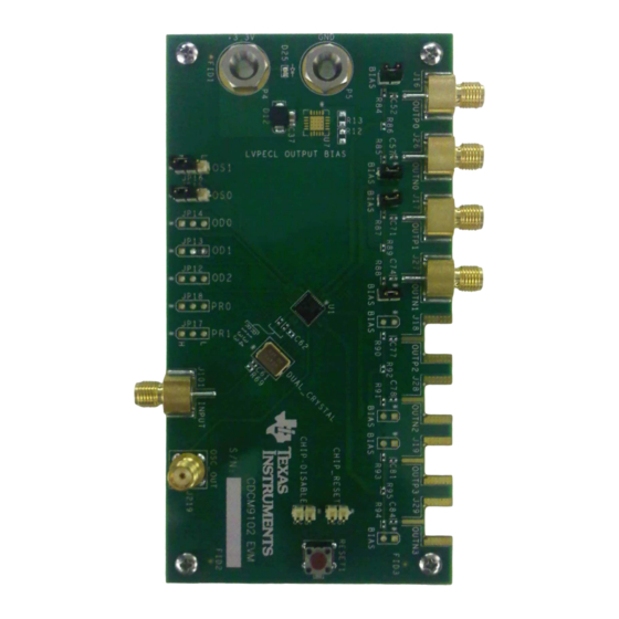
• Termination available for LVPECL, LVDS, and LVCMOS output clocks spacer for space between last listitem and image Figure 1. CDCM9102EVM Evaluation Module General Description The CDCM9102 is a high-performance, low-phase-noise clock generator. The CDCM9102 has one crystal and low-voltage CMOS (LVCMOS) input buffer and two universal outputs. -
Page 3: Signal Path And Control Circuitry
PLL from the other power pins. This EVM can operate from a 3-V to 3.6-V supply voltage. Input Clock Selection The CDCM9102EVM offers the options to use either a crystal or a single-ended clock source as the clock input. Configuring a Crystal Input The EVM is available with an optional 25-MHz crystal. -
Page 4: Configuring A Single-Ended Input
Table 2. Power-Down Configuration OE (Pin 7) Mode Device Core Output Power down Power down Hi-Z Normal Active Active CDCM9102EVM Clock Evaluation Module SCAU048 – March 2012 Submit Documentation Feedback Copyright © 2012, Texas Instruments Incorporated... -
Page 5: Output Buffer Termination
An optional bypassed output (OSC_OUT) is only available if the user chooses the PLL output(s) at an LVPECL signaling level. J219 is the SMA for this output. SCAU048 – March 2012 CDCM9102EVM Clock Evaluation Module Submit Documentation Feedback Copyright © 2012, Texas Instruments Incorporated... -
Page 6: Schematic
Schematic www.ti.com Schematic Figure 5. CDCM9102EVM Schematic CDCM9102EVM Clock Evaluation Module SCAU048 – March 2012 Submit Documentation Feedback Copyright © 2012, Texas Instruments Incorporated... - Page 7 Any exceptions to this are strictly prohibited and unauthorized by Texas Instruments unless user has obtained appropriate experimental/development licenses from local regulatory authorities, which is responsibility of user including its acceptable authorization.
- Page 8 Also, please do not transfer this product, unless you give the same notice above to the transferee. Please note that if you could not follow the instructions above, you will be subject to penalties of Radio Law of Japan. Texas Instruments Japan Limited (address) 24-1, Nishi-Shinjuku 6 chome, Shinjukku-ku, Tokyo, Japan...
- Page 9 This development kit is NOT certified as Confirming to Technical Regulations of Radio Law of Japan http://www.tij.co.jp 【ご使用にあたっての注】 本開発キットは技術基準適合証明を受けておりません。 本製品のご使用に際しては、電波法遵守のため、以下のいずれかの措置を取っていただく必要がありますのでご注意ください。 1. 電波法施行規則第6条第1項第1号に基づく平成18年3月28日総務省告示第173号で定められた電波暗室等の試験設備でご使用いただく。 2. 実験局の免許を取得後ご使用いただく。 3. 技術基準適合証明を取得後ご使用いただく。 なお、本製品は、上記の「ご使用にあたっての注意」を譲渡先、移転先に通知しない限り、譲渡、移転できないものとします。 上記を遵守頂けない場合は、電波法の罰則が適用される可能性があることをご留意ください。 日本テキサス・インスツルメンツ株式会社 東京都新宿区西新宿6丁目24番1号 西新宿三井ビル http://www.tij.co.jp SPACER SPACER SPACER SPACER SPACER SPACER SPACER SPACER SPACER SPACER SPACER...
- Page 10 FDA Class III or similar classification, then you must specifically notify TI of such intent and enter into a separate Assurance and Indemnity Agreement. Mailing Address: Texas Instruments, Post Office Box 655303, Dallas, Texas 75265 Copyright © 2012, Texas Instruments Incorporated...
- Page 11 Any exceptions to this are strictly prohibited and unauthorized by Texas Instruments unless user has obtained appropriate experimental/development licenses from local regulatory authorities, which is responsibility of user including its acceptable authorization.
- Page 12 FCC Interference Statement for Class B EVM devices This equipment has been tested and found to comply with the limits for a Class B digital device, pursuant to part 15 of the FCC Rules. These limits are designed to provide reasonable protection against harmful interference in a residential installation. This equipment generates, uses and can radiate radio frequency energy and, if not installed and used in accordance with the instructions, may cause harmful interference to radio communications.
- Page 13 Also, please do not transfer this product, unless you give the same notice above to the transferee. Please note that if you could not follow the instructions above, you will be subject to penalties of Radio Law of Japan. Texas Instruments Japan Limited (address) 24-1, Nishi-Shinjuku 6 chome, Shinjuku-ku, Tokyo, Japan http://www.tij.co.jp...
- Page 14 FDA Class III or similar classification, then you must specifically notify TI of such intent and enter into a separate Assurance and Indemnity Agreement. Mailing Address: Texas Instruments, Post Office Box 655303, Dallas, Texas 75265 Copyright © 2012, Texas Instruments Incorporated...
- Page 15 IMPORTANT NOTICE Texas Instruments Incorporated and its subsidiaries (TI) reserve the right to make corrections, enhancements, improvements and other changes to its semiconductor products and services per JESD46, latest issue, and to discontinue any product or service per JESD48, latest issue.
Need help?
Do you have a question about the CDCM9102EVM and is the answer not in the manual?
Questions and answers