Table of Contents
Advertisement
Quick Links
NB7L1008MNGEVB
NB7L1008MNG Evaluation
Board User's Manual
Introduction
The NB7L1008 is a high performance differential
1:8 Clock/Data fanout buffer that operates up to
12 Gbps/7 GHz with a 2.5 V or 3.3 V power supply.
ON Semiconductor has developed a "universal" QFN−32
evaluation board and configured it for the NB7L1008. This
evaluation board was designed to provide a flexible and
convenient platform to quickly evaluate, characterize and
verify the operation of the NB7L1008.
This evaluation board manual contains:
•
Information on the NB7L1008 Evaluation Board
•
Test and Measurement Setup Procedures
This manual should be used in conjunction with the device
datasheet, which contains full technical details on the device
specifications and operation.
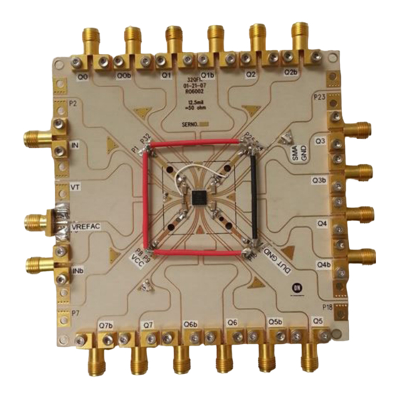
Board Layout
The NB7L1008 Evaluation Board provides a high
bandwidth, 50-W controlled impedance environment and is
implemented in one layer.
Table 1. DIFFERENTIAL INPUTS DRIVEN SINGLE – ENDED
Symbol
V
Single – Ended Input High Voltage
IH
V
Single – Ended Input Low Voltage
IL
V
Input Threshold Reference Voltage Range
th
V
Single – Ended Input Voltage (V
ISE
1. V
, V
, V
and V
parameters must be complied with simultaneously.
th
IH
IL
ISE
2. V
is applied to the complementary input when operating in single-ended mode.
th
Table 2. DIFFERENTIAL INPUTS DRIVEN DIFFERENTIALLY (IN, INB)
Symbol
V
Differential Input High Voltage
IHD
V
Differential Input Low Voltage
ILD
V
Differential Input Voltage (V
ID
I
Input High Current
IH
I
Input Low Current
IL
3. V
, V
, V
and V
parameters must be complied with simultaneously.
IHD
ILD
ID
CMR
If the input signals to the NB7L1008 require termination,
internal 50-W resistors are provided via the VT pin and
grounded using a SMA grounding plug then and should be
stimulated with the appropriate voltage levels.
© Semiconductor Components Industries, LLC, 2014
July, 2017 − Rev. 2
Characteristic
– V
)
IH
IL
Characteristic
– V
)
IHD
ILD
EVAL BOARD USER'S MANUAL
Layer Stack
L1 (Rogers)
High-performance SMA connectors are provided for all
high-speed input & output signal access.
Evaluation Board Assembly Instructions
The QFN−32 evaluation board is designed for
characterizing devices in a 50-W laboratory environment
using high bandwidth equipment.
Output Loading/Termination
LVPECL Outputs
(Notes 1 & 2)
Min
Typ
V
+ 75
−
th
V
−
EE
V
+ 1100
−
EE
200
−
(Note 3)
Min
Typ
V
+ 1100
−
EE
V
−
EE
100
−
−150
40
−150
5
NOTE: For this evaluation board, VT is connected to
ground, thus it can only be used for LVPECL
inputs.
1
www.onsemi.com
Max
Unit
V
mV
CC
V
− 100
mV
th
V
− 100
mV
CC
1200
mV
Max
Unit
V
mV
CC
V
− 100
mV
IHD
1200
mV
+150
mA
+150
mA
Publication Order Number:
EVBUM2241/D
Advertisement
Table of Contents

Subscribe to Our Youtube Channel
Related Manuals for ON Semiconductor NB7L1008MNGEVB


Summary of Contents for ON Semiconductor NB7L1008MNGEVB
- Page 1 1:8 Clock/Data fanout buffer that operates up to www.onsemi.com 12 Gbps/7 GHz with a 2.5 V or 3.3 V power supply. ON Semiconductor has developed a “universal” QFN−32 EVAL BOARD USER’S MANUAL evaluation board and configured it for the NB7L1008. This...
- Page 2 NB7L1008MNGEVB Figure 1. Test Board 1. Connect the appropriate power supplies to V 3. Connect a test measurement device to the device’s DUTGND. output SMA connectors. 2. Connect a signal generator to the input SMA NOTE: The test measurement device must contain 50-W connectors.
- Page 3 NB7L1008MNGEVB Figure 2. Schematic Drawing Table 6. BILL OF MATERIALS Manufacturer Part Number Components Manufacturer Description Web Site SMA Connector Rosenberger High Performance 32K243-40ME3 http://www.rosenberger.de SMA Connector, Side http://www.rosenbergerna.com Launch, Gold Plated SMA Connector Johnson-Emerson SMA Connector, Side 142-0701-801 http://www.digikey.com...
- Page 4 onsemi, , and other names, marks, and brands are registered and/or common law trademarks of Semiconductor Components Industries, LLC dba “onsemi” or its affiliates and/or subsidiaries in the United States and/or other countries. onsemi owns the rights to a number of patents, trademarks, copyrights, trade secrets, and other intellectual property. A listing of onsemi’s product/patent coverage may be accessed at www.onsemi.com/site/pdf/Patent−Marking.pdf.
Need help?
Do you have a question about the NB7L1008MNGEVB and is the answer not in the manual?
Questions and answers