Advertisement
Quick Links
Diagonal 8.923mm (Type 1/1.8) Progressive Scan CCD Image Sensor with Square Pixel for B/W Video Cameras
Description
The ICX274AL is a diagonal 8.923mm (Type 1/1.8)
interline CCD solid-state image sensor with a square
pixel array and 2.01M effective pixels. Progressive
scan allows all pixels' signals to be output
independently within approximately 1/15 second,
and output is also possible using various addition
and pulse elimination methods. This chip features an
electronic shutter with variable charge-storage time
which makes it possible to realize full-frame still
images without a mechanical shutter. Further, high
sensitivity and low dark current are achieved through
the adoption of Super HAD CCD technology.
This chip is suitable for image input applications
such as still cameras which require high resolution,
etc.
Features
• High horizontal and vertical resolution
• Supports the following modes
Progressive scan mode (with/without mechanical shutter)
2/8-line readout mode
2/4-line readout mode
2-line addition mode
Center scan modes (1), (2) and (3)
AF modes (1) and (2)
• Square pixel
• Horizontal drive frequency: 28.6364MHz (typ.), 36.0MHz (max.)
• Reset gate bias are not adjusted
• High sensitivity, low dark current
• Continuous variable-speed shutter function
• Excellent anti-blooming characteristics
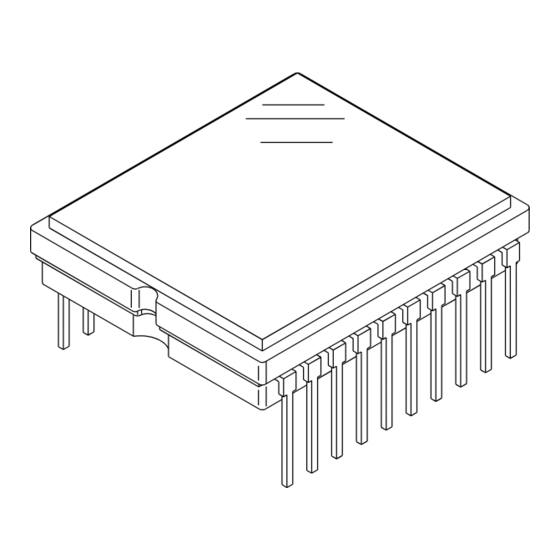
• 20-pin high-precision plastic package
Device Structure
• Interline CCD image sensor
• Image size:
• Total number of pixels:
• Number of effective pixels: 1628 (H) × 1236 (V) approx. 2.01M pixels
• Number of active pixels:
• Recommended number of
recording pixels:
• Chip size:
• Unit cell size:
• Optical black:
• Number of dummy bits:
• Substrate material:
Sony reserves the right to change products and specifications without prior notice. This information does not convey any license by
any implication or otherwise under any patents or other right. Application circuits shown, if any, are typical examples illustrating the
operation of the devices. Sony cannot assume responsibility for any problems arising out of the use of these circuits.
Diagonal 8.923mm (Type 1/1.8)
1688 (H) × 1248 (V) approx. 2.11M pixels
1620 (H) × 1220 (V) approx. 1.98M pixels
1600 (H) × 1200 (V) approx. 1.92M pixels
8.50mm (H) × 6.80mm (V)
4.40µm (H) × 4.40µm (V)
Horizontal (H) direction: Front 12 pixels, rear 48 pixels
Vertical (V) direction:
Horizontal 28
Vertical 1
Silicon
– 1 –
ICX274AL
20 pin DIP (Plastic)
V
12
Pin 11
Optical black position
Front 10 pixels, rear 2 pixels
Pin 1
2
10
H
48
(Top View)
E01X50C34
Advertisement

Related Manuals for Sony ICX274AL


Summary of Contents for Sony ICX274AL
- Page 1 Silicon Sony reserves the right to change products and specifications without prior notice. This information does not convey any license by any implication or otherwise under any patents or other right. Application circuits shown, if any, are typical examples illustrating the operation of the devices.
- Page 2 ICX274AL Block Diagram and Pin Configuration (Top View) Note) Horizontal register Note) : Photo sensor Pin Description Pin No. Symbol Description Pin No. Symbol Description Vφ Vertical register transfer clock Supply voltage φRG Vφ Vertical register transfer clock Reset gate clock Vφ...
- Page 3 ICX274AL Absolute Maximum Ratings Item Ratings Unit Remarks , φRG – φSUB –40 to +12 – φSUB Vφ , Vφ –50 to +15 2α 3α (α = A to C) Against φSUB – φSUB Vφ , Vφ –50 to +0.3 , GND –...
- Page 4 ICX274AL Bias Conditions Item Symbol Min. Typ. Max. Unit Remarks Supply voltage 14.55 15.0 15.45 ∗ Protective transistor bias No line addition ∗ Internally generated value Substrate voltage ∗ 2-line addition ∗ adjustment range 14.4 SUB2 Indicated Indicated Indicated ∆V Substrate voltage adjustment accuracy voltage –...
- Page 5 ICX274AL Clock Voltage Conditions Waveform Item Symbol Min. Typ. Max. Unit Remarks diagram Readout clock 14.55 15.0 15.45 voltage –0.05 0.05 = (V –0.2 0.05 –8.0 –7.5 –7.0 = (V Vφ 8.05 Vφ n – V n (n = 1 to 4) Vertical transfer –...
- Page 6 ICX274AL Clock Equivalent Circuit Constants Item Symbol Min. Typ. Max. Unit Remarks Cφ 3300 Cφ , Cφ 1200 Capacitance between vertical transfer clock and Cφ 2700 Cφ , Cφ 1000 Cφ 1800 Cφ 6800 Cφ V12 (A, B) Cφ V12C Cφ...
- Page 7 ICX274AL Vφ Rφ Rφ Hφ Hφ Cφ Rφ Rφ Hφ Hφ Cφ Cφ Cφ V12α (α = A to C) Cφ V2α4 (α = A to C) Cφ Rφ Cφ Vφ Vφ 2α (α = A to C) 2α (α = A to C) Cφ...
- Page 8 ICX274AL Drive Clock Waveform Conditions (1) Readout clock waveform 100% φM φM (2) Vertical transfer clock waveform Vφ Vφ , Vφ , Vφ Vφ , Vφ , Vφ Vφ = (V = (V Vφ n – V n (n = 1 to 4)
- Page 9 ICX274AL (3) Horizontal transfer clock waveform Hφ 2β Vφ Vφ Hφ 1β Cross-point voltage for the Hφ rising side of the horizontal transfer clocks Hφ and Hφ waveforms is V 1β 1β 2β The overlap period for twh and twl of horizontal transfer clocks Hφ...
- Page 10 ICX274AL Clock Switching Characteristics (Horizontal drive frequency: 28.6364MHz) Item Symbol Unit Remarks Min. Typ. Max. Min. Typ. Max. Min. Typ. Max. Min. Typ. Max. During Readout clock µs readout Vφ , Vφ Vertical transfer ∗ Vφ , Vφ 2α 3α...
- Page 11 ICX274AL Spectral Sensitivity Characteristics (excludes lens characteristics and light source characteristics) 1000 Wave Length [nm] Image Sensor Characteristics (Ta = 25°C) Measurement Item Symbol Min. Typ. Max. Unit Remarks method Sensitivity 1/30s accumulation No line addition ∗ Vsat Saturation signal Ta = 60°C...
- Page 12 ICX274AL Zone Definition of Video Signal Shading 1628 (H) 1236 (V) Zone 0, I Zone II, II’ Ignored region Effective pixel region Measurement System CCD signal output [ ∗ A] Signal output [ ∗ B] C.D.S Note) Adjust the AMP gain so that the gain between [ ∗ A] and [ ∗ B] equals 1.
- Page 13 ICX274AL Readout modes The diagrams below and on the following pages show the output methods for the following nine readout modes. Progressive scan mode 2/8-line readout mode 2/4-line readout mode 16 (V2C/V3C) 16 (V2C/V3C) 16 (V2C/V3C) 15 (V2C/V3C) 15 (V2C/V3C)
- Page 14 ICX274AL 2-line addition mode Center scan mode (1) Center scan mode (2) 16 (V2C/V3C) 16 (V2C/V3C) 16 (V2C/V3C) 15 (V2C/V3C) 15 (V2C/V3C) 15 (V2C/V3C) 14 (V2A/V3A) 14 (V2A/V3A) 14 (V2A/V3A) 13 (V2B/V3B) 13 (V2B/V3B) 13 (V2B/V3B) 12 (V2C/V3C) 12 (V2C/V3C)
- Page 15 ICX274AL Center scan mode (3) AF mode (1) AF mode (2) 16 (V2C/V3C) 16 (V2C/V3C) 16 (V2C/V3C) 15 (V2C/V3C) 15 (V2C/V3C) 15 (V2C/V3C) 14 (V2A/V3A) 14 (V2A/V3A) 14 (V2A/V3A) 13 (V2B/V3B) 13 (V2B/V3B) 13 (V2B/V3B) 12 (V2C/V3C) 12 (V2C/V3C) 12 (V2C/V3C)
- Page 16 ICX274AL Center scan and AF modes Undesired portions (Swept by vertical register high-speed transfer) Picture center cut-out portion Description of Center Scan and AF Mode Operation The center scan and AF modes realize high frame rates by sweeping the top and bottom of the picture with high-speed transfer and cutting out the center of the picture.
- Page 17 ICX274AL Measurement conditions (1) In the following measurements, the device drive conditions are at the typical values of the bias and clock voltage conditions, and the progressive scan readout mode is used. (2) In the following measurements, spot blemishes are excluded and, unless otherwise specified, the optical black level (OB) is used as the reference for the signal output, which is taken as the value measured at point [*B] of the measurement system.
- Page 18 ICX274AL 4. Video signal shading Set to the standard imaging condition II. With the lens diaphragm at F5.6 to F8, adjusting the luminous intensity so that the average value of the signal output is 150mV. Then measure the maximum value (Vmax [mV]) and minimum value (Vmin [mV]) of the G signal output and substitute the values into the following formula.
- Page 19 ICX274AL – 19 –...
- Page 20 ICX274AL – 20 –...
- Page 21 ICX274AL – 21 –...
- Page 22 ICX274AL – 22 –...
- Page 23 ICX274AL – 23 –...
- Page 24 ICX274AL – 24 –...
- Page 25 ICX274AL – 25 –...
- Page 26 ICX274AL – 26 –...
- Page 27 ICX274AL – 27 –...
- Page 28 ICX274AL – 28 –...
- Page 29 ICX274AL – 29 –...
- Page 30 ICX274AL – 30 –...
- Page 31 ICX274AL – 31 –...
- Page 32 ICX274AL – 32 –...
- Page 33 ICX274AL – 33 –...
- Page 34 ICX274AL – 34 –...
- Page 35 ICX274AL – 35 –...
- Page 36 ICX274AL – 36 –...
- Page 37 ICX274AL – 37 –...
- Page 38 ICX274AL – 38 –...
- Page 39 ICX274AL – 39 –...
- Page 40 ICX274AL – 40 –...
- Page 41 ICX274AL – 41 –...
- Page 42 ICX274AL – 42 –...
- Page 43 ICX274AL – 43 –...
- Page 44 ICX274AL – 44 –...
- Page 45 ICX274AL – 45 –...
- Page 46 ICX274AL – 46 –...
- Page 47 ICX274AL – 47 –...
- Page 48 ICX274AL – 48 –...
- Page 49 ICX274AL – 49 –...
- Page 50 ICX274AL – 50 –...
- Page 51 ICX274AL – 51 –...
- Page 52 ICX274AL – 52 –...
- Page 53 ICX274AL – 53 –...
- Page 54 ICX274AL – 54 –...
- Page 55 ICX274AL – 55 –...
- Page 56 ICX274AL – 56 –...
- Page 57 ICX274AL – 57 –...
- Page 58 ICX274AL – 58 –...
- Page 59 ICX274AL – 59 –...
- Page 60 ICX274AL – 60 –...
- Page 61 ICX274AL – 61 –...
- Page 62 ICX274AL – 62 –...
- Page 63 ICX274AL – 63 –...
- Page 64 ICX274AL – 64 –...
- Page 65 ICX274AL – 65 –...
- Page 66 ICX274AL – 66 –...
- Page 67 ICX274AL – 67 –...
- Page 68 ICX274AL – 68 –...
- Page 69 ICX274AL Notes of Handling 1) Static charge prevention CCD image sensors are easily damaged by static discharge. Before handling be sure to take the following protective measures. a) Either handle bare handed or use non-chargeable gloves, clothes or material. Also use conductive shoes.
- Page 70 ICX274AL c) The adhesive may cause the marking on the rear surface to disappear, especially in case the regulated voltage value is indicated on the rear surface. Therefore, the adhesive should not be applied to this area, and indicated values should be transferred to other locations as a precaution.
- Page 71 ICX274AL Sony Corporation – 71 –...
Need help?
Do you have a question about the ICX274AL and is the answer not in the manual?
Questions and answers