Advertisement
Quick Links
This user's guide describes the characteristics, operation, and use of the evaluation module (EVM) for the
PGA281. This document also includes the schematic, printed circuit board (PCB) layout, and a bill of
materials (BOM). Throughout this document the terms evaluation board, evaluation module, and EVM are
synonymous with the PGA281EVM.
1
Introduction
2
PGA281EVM Hardware
3
Bill of Materials
4
Related Documentation from Texas Instruments
1
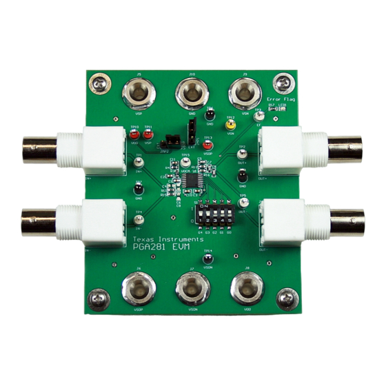
PGA281EVM
2
PGA281EVM Schematic
3
PGA281EVM Default Jumper Settings
4
Top Layer (Signal and Ground)
5
Layer 2 (Power)
6
Layer 3 (Power)
7
Bottom Layer (Power and Ground)
dit.SBOU130 – May 2013
Submit Documentation Feedback
..................................................................................................................
....................................................................................................
.............................................................................................................
................................................................................................................
...................................................................................................
...................................................................................
...........................................................................................
.............................................................................................................
............................................................................................................
.....................................................................................
Copyright © 2013, Texas Instruments Incorporated
Contents
.....................................................................
List of Figures
User's Guide
dit.SBOU130 – May 2013
PGA281EVM
2
3
12
13
2
3
4
8
9
10
11
1
PGA281EVM
Advertisement

Subscribe to Our Youtube Channel
Related Manuals for Texas Instruments PGA281EVM


Summary of Contents for Texas Instruments PGA281EVM
- Page 1 PGA281EVM Schematic ................... PGA281EVM Default Jumper Settings ................... Top Layer (Signal and Ground) ......................Layer 2 (Power) ......................Layer 3 (Power) ..................Bottom Layer (Power and Ground) dit.SBOU130 – May 2013 PGA281EVM Submit Documentation Feedback Copyright © 2013, Texas Instruments Incorporated...
- Page 2 The high supply voltage and excellent common-mode rejection comply with the requirements for universal industrial signal front-ends. PGA281EVM The PGA281EVM provides basic functional evaluation of the PGA281, along with the following features: • Onboard power management circuitry generates all required power-supply rails from one split-supply input •...
- Page 3 PGA281EVM Hardware www.ti.com PGA281EVM Hardware This section discusses the PGA281EVM hardware schematics and PCB layout. Schematic The schematic of the PGA281EVM is shown in Figure Input Connections PGA281 Output Connections VOCM Divider Gain Select Gain Table G3:G0 G4=0 G4=1 0000 0.125...
- Page 4 PGA281EVM Hardware www.ti.com Jumper Settings The PGA281EVM jumper settings are given in Table 1. The default settings are shown in Figure Figure 3. PGA281EVM Default Jumper Settings Table 1. PGA281EVM Jumper Settings Jumper Position Function VSOP provided by onboard low dropout (LDO)
- Page 5 2.3.4 Onboard LDO Regulator The PGA281EVM contains an onboard LDO regulator (U2) that is used to generate VSOP and VDD from VSP. This configuration greatly simplifies the power connections to the PGA281EVM, because then only VSP, VSN, and GND must be provided. The LDO regulator output voltage can be adjusted by replacing resistor R20.
- Page 6 J1 (IN+) and J3 (IN–), while the output signal is measured at BNC connectors J2 (OUT+) and J4 (OUT–). VOCM VOCM controls the output stage common-mode voltage. On the PGA281EVM, a resistive voltage divider created by R3 and R4 sets VOCM equal to (VSOP/2). Gain Select Switch S1 controls the PGA281 gain.
- Page 7 PGA281EVM PCB layout. NOTE: Board layouts are not to scale. These figures are intended to show how the board is laid out; they are not intended to be used for manufacturing PGA281EVM PCBs. dit.SBOU130 – May 2013...
- Page 8 PGA281EVM Hardware www.ti.com Figure 4. Top Layer (Signal and Ground) PGA281EVM dit.SBOU130 – May 2013 Submit Documentation Feedback Copyright © 2013, Texas Instruments Incorporated...
- Page 9 PGA281EVM Hardware www.ti.com Figure 5. Layer 2 (Power) dit.SBOU130 – May 2013 PGA281EVM Submit Documentation Feedback Copyright © 2013, Texas Instruments Incorporated...
- Page 10 PGA281EVM Hardware www.ti.com Figure 6. Layer 3 (Power) PGA281EVM dit.SBOU130 – May 2013 Submit Documentation Feedback Copyright © 2013, Texas Instruments Incorporated...
- Page 11 PGA281EVM Hardware www.ti.com Figure 7. Bottom Layer (Power and Ground) dit.SBOU130 – May 2013 PGA281EVM Submit Documentation Feedback Copyright © 2013, Texas Instruments Incorporated...
- Page 12 Bill of Materials www.ti.com Bill of Materials Table 6 gives the bill of materials (BOM) used for the PGA281EVM. It also lists examples of optional components. Table 6. PGA281EVM Bill of Materials Count RefDes Value Description Part Number Manufacturer PGA281, TSSOP-16...
- Page 13 The following documents provide information regarding Texas Instruments' integrated circuits and support tools for the PGA281EVM. This user's guide is available from the TI web site under literature number SBOU130. Any letter appended to the literature number corresponds to the document revision that is current at the time of the writing of this document.
- Page 14 Any exceptions to this are strictly prohibited and unauthorized by Texas Instruments unless user has obtained appropriate experimental/development licenses from local regulatory authorities, which is responsibility of user including its acceptable authorization.
- Page 15 FCC Interference Statement for Class B EVM devices This equipment has been tested and found to comply with the limits for a Class B digital device, pursuant to part 15 of the FCC Rules. These limits are designed to provide reasonable protection against harmful interference in a residential installation. This equipment generates, uses and can radiate radio frequency energy and, if not installed and used in accordance with the instructions, may cause harmful interference to radio communications.
- Page 16 Also, please do not transfer this product, unless you give the same notice above to the transferee. Please note that if you could not follow the instructions above, you will be subject to penalties of Radio Law of Japan. Texas Instruments Japan Limited (address) 24-1, Nishi-Shinjuku 6 chome, Shinjuku-ku, Tokyo, Japan http://www.tij.co.jp...
- Page 17 FDA Class III or similar classification, then you must specifically notify TI of such intent and enter into a separate Assurance and Indemnity Agreement. Mailing Address: Texas Instruments, Post Office Box 655303, Dallas, Texas 75265 Copyright © 2013, Texas Instruments Incorporated...
- Page 18 IMPORTANT NOTICE Texas Instruments Incorporated and its subsidiaries (TI) reserve the right to make corrections, enhancements, improvements and other changes to its semiconductor products and services per JESD46, latest issue, and to discontinue any product or service per JESD48, latest issue.
- Page 19 Mouser Electronics Authorized Distributor Click to View Pricing, Inventory, Delivery & Lifecycle Information: Texas Instruments PGA281EVM...
Need help?
Do you have a question about the PGA281EVM and is the answer not in the manual?
Questions and answers