Table of Contents
Advertisement
Quick Links
RF-BM-ND10
www.szrfstar.com
V1.0 - May, 2023
RF-BM-ND10 nRF52833
Bluetooth 5.3 Low Energy, Bluetooth mesh, NFC,
Thread and ZigBee Wireless Module
Version 1.0
Shenzhen RF-star Technology Co., Ltd.
May 25
th
, 2023
All rights reserved. Those responsible for unauthorized reproduction will be prosecuted.
Shenzhen RF-star Technology Co., Ltd.
Page 1 of 24
Advertisement
Table of Contents

Related Manuals for RF-Star RF-BM-ND10


Summary of Contents for RF-Star RF-BM-ND10
- Page 1 RF-BM-ND10 nRF52833 Bluetooth 5.3 Low Energy, Bluetooth mesh, NFC, Thread and ZigBee Wireless Module Version 1.0 Shenzhen RF-star Technology Co., Ltd. May 25 , 2023 All rights reserved. Those responsible for unauthorized reproduction will be prosecuted. Shenzhen RF-star Technology Co., Ltd.
-
Page 2: Device Overview
V1.0 - May, 2023 1 Device Overview 1.1 Description RF-BM-ND10 is a multiprotocol Radio Frequency module based on Nordic nRF52833 SoC. It integrates a 32 MHz crystal, 512 KB Flash, and 128 KB RAM. Its 64 MHz ARM ® Cortex ®... -
Page 3: Applications
Power Supply 1.7 V ~ 3.6 V Figure 1. Functional Block Diagram of RF-BM-ND10 1.5 Part Number Conventions The part numbers are of the form of RF-BM-ND10 where the fields are defined as follows: Company Name Module Version The 10... -
Page 4: Table Of Contents
4.7.1 Unsatisfactory Transmission Distance ..................18 4.7.2 Vulnerable Module ..........................18 4.7.3 High Bit Error Rate ..........................18 4.8 Electrostatics Discharge Warnings ......................19 4.9 Soldering and Reflow Condition ......................... 19 Shenzhen RF-star Technology Co., Ltd. Page 4 of 24... - Page 5 RF-BM-ND10 www.szrfstar.com V1.0 - Dec., 2022 5 Optional Package Specification ..........................21 6 Revision History ................................23 7 Contact Us ..................................24 Shenzhen RF-star Technology Co., Ltd. Page 5 of 24...
-
Page 6: Module Configuration And Functions
RF-BM-ND10 www.szrfstar.com V1.0 - Dec., 2022 2 Module Configuration and Functions 2.1 Module Parameters Table 1. Parameters of RF-BM-ND10 Chipset nRF52833-QIAA Supply Power Voltage 1.7 V ~ 3.6 V, recommended to 3.3 V Frequency 2402 MHz ~ 2480 MHz Transmit Power -20 dBm ~ +8.0 dBm... -
Page 7: Module Pin Diagram
RF-BM-ND10 www.szrfstar.com V1.0 - Dec., 2022 2.2 Module Pin Diagram Figure 3. Pin Diagram of RF-BM-ND10 2.3 Pin Functions Table 2. Pin Functions of RF-BM-ND10 Name Chip Pin Function Description P0.09 Digital I/O General purpose I/O P0_09 NFC1 NFC input NFC antenna connection P0.10... - Page 8 Trace data Trace buffer TRACEDATA[2] TRACEDATA2 P0.12 Digital I/O General purpose I/O P0_12 Trace data Trace buffer TRACEDATA[1] TRACEDATA1 USB Power 5 V input for USB 3.3 V regulator VBUS VBUS Shenzhen RF-star Technology Co., Ltd. Page 8 of 24...
- Page 9 Digital I/O General purpose I/O P1_02 P1.02 Digital I/O General purpose I/O P1_04 P1.04 P1_06 P1.06 Digital I/O General purpose I/O Digital I/O General purpose I/O P1_07 P1.07 Half-hole ANT pin Shenzhen RF-star Technology Co., Ltd. Page 9 of 24...
-
Page 10: Specifications
Functional operation does not guarantee performance beyond the limits of the conditional parameter values in the table below. Long-term work beyond this limit will affect the reliability of the module more or less. Table 3. Recommended Operating Conditions of RF-BM-ND10 Items Condition Min. -
Page 11: Application, Implementation, And Layout
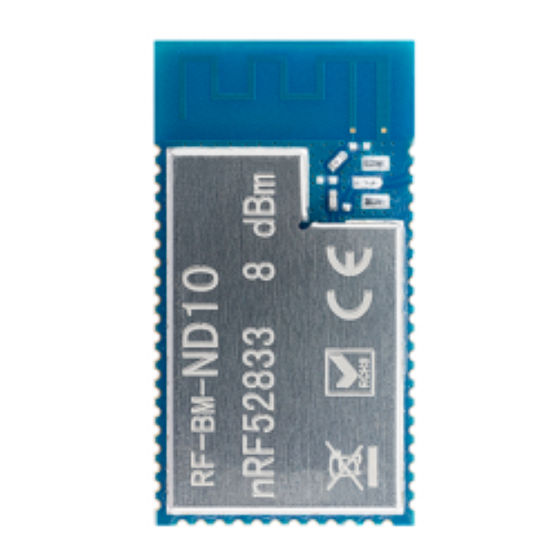
RF-BM-ND10 www.szrfstar.com V1.0 - Dec., 2022 4 Application, Implementation, and Layout 4.1 Module Photos Figure 4. Photos of RF-BM-ND10 4.2 Recommended PCB Footprint Figure 5. Recommended PCB Footprint of RF-BM-ND10 (mm) Shenzhen RF-star Technology Co., Ltd. Page 11 of 24... -
Page 12: Schematic Diagram
RF-BM-ND10 www.szrfstar.com V1.0 - Dec., 2022 4.3 Schematic Diagram Figure 6. Schematic Diagram of RF-BM-ND10 Shenzhen RF-star Technology Co., Ltd. Page 12 of 24... -
Page 13: Reference Design
RF-BM-ND10 www.szrfstar.com V1.0 - Dec., 2022 4.4 Reference Design Figure 7. Reference Design of RF-BM-ND10 Shenzhen RF-star Technology Co., Ltd. Page 13 of 24... -
Page 14: Antenna
Note: The hollow-out position is based on the antenna used. 4.5.2 Antenna Output Mode Modification 1. RF-BM-ND10 has three antenna output modes. An onboard PCB antenna, a stamp half-hole output (ANT pin, see pin function table for details) and one IPEX connecter. -
Page 15: External Antenna Design Recommendation Of The Half-Hole Ant Pin
V1.0 - Dec., 2022 Figure 9. Antenna Output Mode Change of RF-BM-ND10 4.5.3 External Antenna Design Recommendation of the Half-Hole ANT Pin 1. A Π-type matching circuit is reserved for the antenna, and 50 Ω impedance control is performed on the RF traces. -
Page 16: Ipex Connector Specification
0.8254 mm, and the spacing between traces and copper is 0.22 mm. Figure 12. SI9000 Impedance Calculation Diagram 4.5.4 IPEX Connector Specification RF-BM-ND10 module can be integrated with the IPEX version 1 antenna seat, the specification of the antenna seat is as follows: Figure 13. Specification of Antenna Seat Shenzhen RF-star Technology Co., Ltd. -
Page 17: Basic Operation Of Hardware Design
6. Assuming that there are devices with large electromagnetic interference around the module, which will greatly affect the module performance. It is recommended to stay away from the module according to the strength of the Shenzhen RF-star Technology Co., Ltd. Page 17 of 24... -
Page 18: Trouble Shooting
4.7.3 High Bit Error Rate 1. There are co-channel signal interferences nearby. It is recommended to be away from the interference sources or modify the frequency and channel to avoid interferences. Shenzhen RF-star Technology Co., Ltd. Page 18 of 24... -
Page 19: Electrostatics Discharge Warnings
3. If the extension wire or feeder wire is of poor quality or too long, the bit error rate will be high. 4.8 Electrostatics Discharge Warnings The module will be damaged by the discharge of static. RF-star suggests that all modules should follow the 3 precautions below: 1. - Page 20 RF-BM-ND10 www.szrfstar.com V1.0 - Dec., 2022 Figure 15. Recommended Reflow for Lead-Free Solder Shenzhen RF-star Technology Co., Ltd. Page 20 of 24...
- Page 21 The default package method is . If you need the modules to be shipped by tape & reel, pls contact us in advance. Figure 16. Default Package by Tray Shenzhen RF-star Technology Co., Ltd. Page 21 of 24...
- Page 22 RF-BM-ND10 www.szrfstar.com V1.0 - Dec., 2022 Figure 17. Package by Tape & Reel Shenzhen RF-star Technology Co., Ltd. Page 22 of 24...
- Page 23 1. The document will be optimized and updated from time to time. Before using this document, please make sure it is the latest version. 2. To obtain the latest document, please download it from the official website: www.rfstariot.com and www.szrfstar.com. Shenzhen RF-star Technology Co., Ltd. Page 23 of 24...
- Page 24 RF-BM-ND10 www.szrfstar.com V1.0 - Dec., 2022 7 Contact Us SHENZHEN RF-STAR TECHNOLOGY CO., LTD. Shenzhen HQ: Add.: Room 502, Podium Building No. 12, Shenzhen Bay Science and Technology Ecological Park, Nanshan District, Shenzhen, Guangdong, China, 518063 Tel.: 86-755-8632 9829 Chengdu Branch: Add.: N2-1604, Global Center, North No.
Need help?
Do you have a question about the RF-BM-ND10 and is the answer not in the manual?
Questions and answers