Table of Contents

Related Manuals for RF-Star RF-BM-ND04C


Summary of Contents for RF-Star RF-BM-ND04C
- Page 1 RF-BM-ND04C and RF-BM-ND04CI nRF52810 Bluetooth 5.0 Low Energy Module Version 1.1 Shenzhen RF-star Technology Co., Ltd. May 26 , 2023 All rights reserved. Those responsible for unauthorized reproduction will be prosecuted.
-
Page 2: Device Overview
1 Device Overview 1.1 Module Series There is a series of RF-BM-ND04C(I) Bluetooth 5.0 Low Energy modules. All of them are based on Nordic nRF52810 SoC. Those modules are pin-to-pin compatible with each other as well. Table 1. Module Series of RF-BM-ND04(I) -
Page 3: Applications
32.0 MHz 32.768 kHz Half- hole GPIO nRF5281 Debug Antenna LC Filter Antenna IPEX Matching Switch Connect Power Supply Reset 1.7 V ~ 3.6 V RF-BM-ND04CI Figure 1. Functional Block Diagram of RF-BM-ND04C(I) Shenzhen RF-star Technology Co., Ltd. Page 2 of 27... -
Page 4: Part Number Conventions
RF-BM-ND04C(I) www.szrfstar.com V1.1 - May, 2023 1.6 Part Number Conventions The part numbers are of the form of RF-BM-ND04C(I) where the fields are defined as follows: 04C(I) Company Name Module Version Without I: nRF52810 PCB Version RF-STAR With I: nRF52810 IPEX Version... -
Page 5: Table Of Contents
4.6 Basic Operation of Hardware Design ...................... 18 4.7 Trouble Shooting .............................. 19 4.7.1 Unsatisfactory Transmission Distance ..................19 4.7.2 Vulnerable Module ..........................20 4.7.3 High Bit Error Rate ..........................20 4.8 Electrostatics Discharge Warnings ......................20 Shenzhen RF-star Technology Co., Ltd. Page 4 of 27... - Page 6 5 Optional Package Specification ..........................22 6 Certification ..................................24 6.1 SRRC ................................... 24 6.2 FCC ..................................24 6.3 RoHS ..................................25 7 Revision History ................................26 8 Contact Us ..................................27 Shenzhen RF-star Technology Co., Ltd. Page 5 of 27...
-
Page 7: Module Configuration And Functions
RF-BM-ND04C(I) www.szrfstar.com V1.1 - May, 2023 2 Module Configuration and Functions 2.1 Module Parameters Table 2. Parameters of RF-BM-ND04C(I) Chipset nRF52810 Supply Power Voltage 1.7 V ~ 3.6 V, recommended to 3.3 V Frequency 2402 MHz ~ 2480 MHz Transmit Power -20.0 dBm ~ +4.0 dBm (typical: 0 dBm) -
Page 8: Module Pin Diagram
RF-BM-ND04C(I) www.szrfstar.com V1.1 - May, 2023 2.2 Module Pin Diagram RF-BM-ND04C RF-BM-ND04CI Figure 3. Pin Diagram of RF-BM-ND04C(I) 2.3 Pin Functions Table 3. Pin Functions of RF-BM-ND04C Name Chip Pin Pin Type Description Power Power supply 1.7 V ~ 3.6 V, Recommend to 3.3 V General purpose I/O P0.21... - Page 9 Digital I/O General purpose I/O P0.14 Digital I/O General purpose I/O General purpose I/O P0.15 Digital I/O P0.16 Digital I/O General purpose I/O Serial wire debug debugging SWDIO SWDIO Digital I/O programming Shenzhen RF-star Technology Co., Ltd. Page 8 of 27...
- Page 10 Analog input SAADC/COMP input General purpose I/O Digital I/O P0.30/AIN6 Analog input SAADC/COMP input P0.26 Digital I/O General purpose I/O P0.27 Digital I/O General purpose I/O P0.02/AIN0 Digital I/O General purpose I/O Shenzhen RF-star Technology Co., Ltd. Page 9 of 27...
- Page 11 Serial wire debug clock input for debugging and SWCLK SWDCLK Digital input programming General purpose I/O P0.17 Digital I/O General purpose I/O P0.18 Digital I/O P0.19 Digital I/O General purpose I/O General purpose I/O P0.20 Digital I/O Shenzhen RF-star Technology Co., Ltd. Page 10 of 27...
-
Page 12: Specifications
Functional operation does not guarantee performance beyond the limits of the conditional parameter values in the table below. Long-term work beyond this limit will affect the reliability of the module more or less. Table 5. Recommended Operating Conditions of RF-BM-ND04C(I) Items Condition Min. -
Page 13: Application, Implementation, And Layout
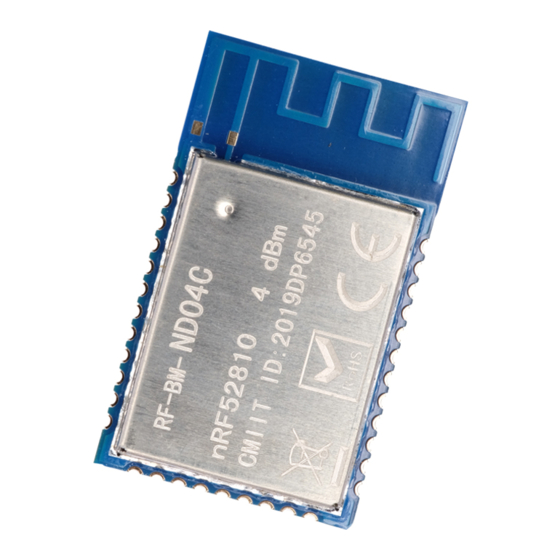
RF-BM-ND04C(I) www.szrfstar.com V1.1 - May, 2023 4 Application, Implementation, and Layout 4.1 Module Photos RF-BM-ND04C RF-BM-ND04CI Figure 4. Photos of RF-BM-ND04C(I) 4.2 Recommended PCB Footprint RF-BM-ND04C Shenzhen RF-star Technology Co., Ltd. Page 12 of 27... -
Page 14: Schematic Diagram
RF-BM-ND04C(I) www.szrfstar.com V1.1 - May, 2023 RF-BM-ND04CI Figure 5. Recommended PCB Footprint of RF-BM-ND04C(I) (mm) 4.3 Schematic Diagram RF-BM-ND04C Shenzhen RF-star Technology Co., Ltd. Page 13 of 27... -
Page 15: Reference Design
RF-BM-ND04C(I) www.szrfstar.com V1.1 - May, 2023 RF-BM-ND04CI Figure 6. Schematic Diagram of RF-BM-ND04C(I) 4.4 Reference Design Note: EN falling edge active. RF-BM-ND04C Shenzhen RF-star Technology Co., Ltd. Page 14 of 27... -
Page 16: Antenna
V1.1 - May, 2023 Note: EN falling edge active. RF-BM-ND04CI Figure 7. Reference Design of RF-BM-ND04C(I) 4.5 Antenna 4.5.1 Antenna Design Recommendation 1. The antenna installation structure has a great influence on the module performance. It is necessary to ensure the antenna is exposed and preferably vertically upward. -
Page 17: Ipex Connector
Note: The hollow-out position is based on the antenna used. 4.5.2 IPEX Connector RF-BM-ND04CI module is integrated the IPEX version 1 antenna seat, the specification of the antenna seat is as follow: Figure 9. Specification of Antenna Seat Shenzhen RF-star Technology Co., Ltd. Page 16 of 27... -
Page 18: Antenna Output Mode Modification
4.5.4 External Antenna Design Recommendation of the Half-Hole ANT Pin 1. A Π-type matching circuit is reserved for the antenna, and 50 Ω impedance control is performed on the RF traces. Shenzhen RF-star Technology Co., Ltd. Page 17 of 27... -
Page 19: Basic Operation Of Hardware Design
1. It is recommended to offer the module with a DC stabilized power supply, a tiny power supply ripple coefficient, and reliable ground. Please pay attention to the correct connection between the positive and negative poles of the power Shenzhen RF-star Technology Co., Ltd. Page 18 of 27... -
Page 20: Trouble Shooting
4. The incorrect power register set or the high data rate in an open-air may shorten the communication distance. The higher the data rate, the closer the distance. 5. The low voltage of the power supply is lower than the recommended value at ambient temperature, and the lower Shenzhen RF-star Technology Co., Ltd. Page 19 of 27... -
Page 21: Vulnerable Module
3. If the extension wire or feeder wire is of poor quality or too long, the bit error rate will be high. 4.8 Electrostatics Discharge Warnings The module will be damaged for the discharge of static. RF-star suggests that all modules should follow the 3 precautions below: 1. - Page 22 Max. 6 ℃/s Time from 25 ℃ to Peak Temperature (t Max. 6 minutes Max. 8 minutes Time of Soldering Zone (t 20±10 s 20±10 s Figure 15. Recommended Reflow for Lead-Free Solder Shenzhen RF-star Technology Co., Ltd. Page 21 of 27...
-
Page 23: Optional Package Specification
The default package method is . If you need the modules to be shipped by tape & reel, pls contact us in advance. Figure 16. Default Package by Tray Shenzhen RF-star Technology Co., Ltd. Page 22 of 27... - Page 24 RF-BM-ND04C(I) www.szrfstar.com V1.1 - May, 2023 Figure 17. Package by Tape & Reel Shenzhen RF-star Technology Co., Ltd. Page 23 of 27...
-
Page 25: Certification
V1.1 - May, 2023 6 Certification 6.1 SRRC SRRC ID: 2019DP6545 Figure 18. SRRC Certificate of RF-BM-ND04C 6.2 FCC Warnings: This device complies with part 15 of the FCC Rules. Operation is subject to the following two conditions: (1) This device may not cause harmful interference, and (2) this device must accept any interference received, including interference that may cause undesired operation. -
Page 26: Rohs
RF-BM-ND04C(I) www.szrfstar.com V1.1 - May, 2023 6.3 RoHS RoHS Report No.: C210302063001 Figure 20. RoHS Certificate of RF-BM-ND04C Shenzhen RF-star Technology Co., Ltd. Page 25 of 27... -
Page 27: Revision History
1. The document will be optimized and updated from time to time. Before using this document, please make sure it is the latest version. 2. To obtain the latest document, please download it from the official website: www.rfstariot.com and www.szrfstar.com. Shenzhen RF-star Technology Co., Ltd. Page 26 of 27... -
Page 28: Contact Us
RF-BM-ND04C(I) www.szrfstar.com V1.1 - May, 2023 8 Contact Us SHENZHEN RF-STAR TECHNOLOGY CO., LTD. Shenzhen HQ: Add.: C601, Skyworth Building, High-tech Park, Nanshan District, Shenzhen, Guangdong, China, 518057 Tel.: 86-755-3695 3756 Chengdu Branch: Add.: B3-03, Building No.1, Incubation Park, High-Tech District, Chengdu, Sichuan, China, 610041 Tel.: 86-28-6577 5970...
Need help?
Do you have a question about the RF-BM-ND04C and is the answer not in the manual?
Questions and answers