
Related Manuals for RF-Star RF-BM-ND06


Summary of Contents for RF-Star RF-BM-ND06
- Page 1 RF-BM-ND06 Bluetooth 5.0 Low Energy Module Version 1.0 Shenzhen RF-star Technology Co., Ltd. Sep. 22 , 2020...
-
Page 2: Nordic Ble Module List
1. The communication distance is the longest distance obtained by testing the module's maximum transmission power in an open and interference-free environment in sunny weather. 2. Click the picture to buy modules. Shenzhen RF-star Technology Co., Ltd. Page 1 of 22... -
Page 3: Nrf52 Series
15.2 11.2 RF-BM-ND08I IPEX Contact me 15 24.8 RF-BM-ND04C 15 24.8 RF-BM-ND04CI IPEX nRF52810 15.2 11.2 RF-BM-ND08C 15.2 11.2 RF-BM-ND08CI IPEX Contact me RF-BM-ND04A nRF52811 24.8 Shenzhen RF-star Technology Co., Ltd. Page 2 of 22... - Page 4 1. The communication distance is the longest distance obtained by testing the module's maximum transmission power in an open and interference-free environment in sunny weather. 2. Click the picture to buy modules. Shenzhen RF-star Technology Co., Ltd. Page 3 of 22...
-
Page 5: Device Overview
V1.0 - Sep., 2020 1 Device Overview 1.1 Description RF-BM-ND06 is an RF module based on Nordic multiprotocol SoC nRF52840-QIAA-R with best-in-class 32-bit ARM ® Cortex -M4 processor. It integrates a 32.768 kHz and a 32 MHz crystal, a power filter, an antenna matching, and a high- ®... -
Page 6: Functional Block Diagram
Reset 1.7 V ~ 5.5 V Figure 1. Functional Block Diagram of RF-BM-ND06 1.5 Part Number Conventions The part numbers are of the form of RF-BM-ND06 where the fields are defined as follows: Company Name Module Version nRF52840 Second Version... -
Page 7: Table Of Contents
4.5 Basic Operation of Hardware Design ...................... 15 4.6 Trouble Shooting .............................. 16 4.6.1 Unsatisfactory Transmission Distance ..................16 4.6.2 Vulnerable Module ..........................16 4.6.3 High Bit Error Rate ..........................17 4.7 Electrostatics Discharge Warnings ......................17 Shenzhen RF-star Technology Co., Ltd. Page 6 of 22... -
Page 8: Table Of Figures
Figure 3. Pin Diagram of RF-BM-ND06 ......................9 Figure 4. Photos of RF-BM-ND06 ........................13 Figure 5. Recommended PCB Footprint of RF-BM-ND06 (mm) ............13 Figure 6. Schematic Diagram of RF-BM-ND06 ................... 14 Figure 7. Reference Design of RF-BM-ND06 ....................14 Figure 8. -
Page 9: Module Configuration And Functions
RF-BM-ND06 www.szrfstar.com V1.0 - Sep., 2020 2 Module Configuration and Functions 2.1 Module Parameters Table 1. Parameters of RF-BM-ND06 Chipset nRF52840QIAA-R Supply Power Voltage 1.7 V ~ 5.5 V, recommended to 3.3 V Frequency 2402 MHz ~ 2480 MHz Transmit Power -20.0 dBm ~ +8.0 dBm (typical: 0 dBm) -
Page 10: Module Pin Diagram
RF-BM-ND06 www.szrfstar.com V1.0 - Sep., 2020 2.2 Module Pin Diagram Figure 3. Pin Diagram of RF-BM-ND06 2.3 Pin Functions Table 2. Pin Functions of RF-BM-ND06 Name Chip Pin Pin Type Description P0.12 SIO_12 Power 1.7 V ~ 3.6 V 1.7 V ~ 3.6 V VDD_HV Power 2.5 V ~ 5.5 V... - Page 11 P1.01 GPIO_1.02 P1.02 FTDI USB_DTR via jumper on nAutoRUN nAutoRUN P1.03 J12pin1-2. GPIO_1.04 P1.04 GPIO_1.05 P1.05 GPIO_1.06 P1.06 RF-interface RF_OUT GPIO_1.07 P1.07 GPIO_1.10 P1.10 GPIO_1.11 P1.11 GPIO_1.12 SPI_CS P1.12 GPIO_1.13 P1.13 Shenzhen RF-star Technology Co., Ltd. Page 10 of 22...
- Page 12 MOSI and CLK are outputs when in SPI master mode P0.05 GPIO_0.05 UART_RTS P0.06 GPIO_0.06 UART_TX GPIO_0.07 UART_CTS P0.07 P0.08 GPIO_0.08 UART_RX GPIO_1.08 SPI_MOSI P1.08 P1.09 GPIO_1.09 SPI_CLK P0.11 GPIO_0.11 Shenzhen RF-star Technology Co., Ltd. Page 11 of 22...
-
Page 13: Specifications
Functional operation does not guarantee performance beyond the limits of the conditional parameter values in the table below. Long-term work beyond this limit will affect the reliability of the module more or less. Table 3. Recommended Operating Conditions of RF-BM-ND06 Items Condition Min. -
Page 14: Application, Implementation, And Layout
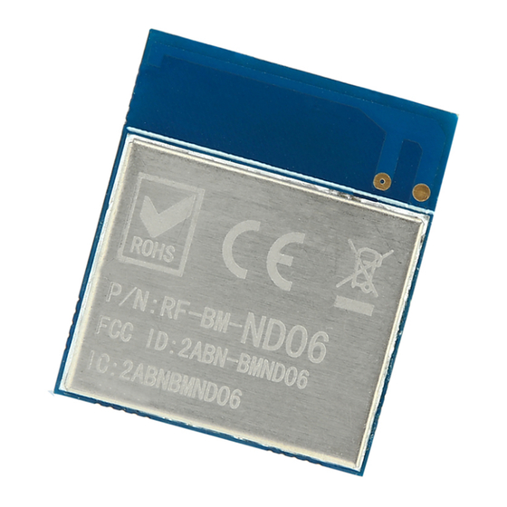
RF-BM-ND06 www.szrfstar.com V1.0 - Sep., 2020 4 Application, Implementation, and Layout 4.1 Module Photos Figure 4. Photos of RF-BM-ND06 4.2 Recommended PCB Footprint Figure 5. Recommended PCB Footprint of RF-BM-ND06 (mm) Shenzhen RF-star Technology Co., Ltd. Page 13 of 22... -
Page 15: Schematic Diagram
RF-BM-ND06 www.szrfstar.com V1.0 - Sep., 2020 4.3 Schematic Diagram Figure 6. Schematic Diagram of RF-BM-ND06 4.4 Reference Design Figure 7. Reference Design of RF-BM-ND06 Shenzhen RF-star Technology Co., Ltd. Page 14 of 22... -
Page 16: Basic Operation Of Hardware Design
The inverted-F antenna position on PCB is free space electromagnetic radiation. The location and layout of antenna is a key factor to increase the data rate and transmission range. Therefore, the layout of the module antenna location and routing is recommended as follows: Shenzhen RF-star Technology Co., Ltd. Page 15 of 22... -
Page 17: Trouble Shooting
1. Please ensure the supply voltage is between the recommended values. The module will be permanently damaged if the voltage exceeds the maximum value. Please ensure the stable power supply and no frequently fluctuated Shenzhen RF-star Technology Co., Ltd. Page 16 of 22... -
Page 18: High Bit Error Rate
3. If the extension wire or feeder wire is of poor quality or too long, the bit error rate will be high. 4.7 Electrostatics Discharge Warnings The module will be damaged for the discharge of static. RF-star suggest that all modules should follow the 3 precautions below: 1. -
Page 19: Optional Packaging
Max. 8 minutes 20±10 s 20±10 s Time of Soldering Zone (t Figure 9. Recommended Reflow for Lead Free Solder 4.9 Optional Packaging Figure 10. Optional Packaging Mode Note: Default tray packaging. Shenzhen RF-star Technology Co., Ltd. Page 18 of 22... -
Page 20: Certification
This device complies with part 15 of the FCC Rules. Operation is subject to the following two conditions: (1) This device may not cause harmful interference, and (2) this device must accept any interference received, including interference that may cause undesired operation. FCC ID: 2ABN2-RF-BM-ND06 Figure 12. FCC Certificate Shenzhen RF-star Technology Co., Ltd. Page 19 of 22... -
Page 21: Figure 13. Ce Certificate
RF-BM-ND06 www.szrfstar.com V1.0 - Sep., 2020 5.3 CE Figure 13. CE Certificate Shenzhen RF-star Technology Co., Ltd. Page 20 of 22... -
Page 22: Revision History
1. The document will be optimized and updated from time to time. Before using this document, please make sure it is the latest version. 2. To obtain the latest document, please download it from the official website: www.szrfstar.com. Shenzhen RF-star Technology Co., Ltd. Page 21 of 22... -
Page 23: Contact Us
RF-BM-ND06 www.szrfstar.com V1.0 - Sep., 2020 7 Contact Us SHENZHEN RF-STAR TECHNOLOGY CO., LTD. Shenzhen HQ: Add.: Room 601, Block C, Skyworth Building, High-tech Park, Nanshan District, Shenzhen, Guangdong, China Tel.: 86-755-3695 3756 Chengdu Branch: Add.: No. B3-03, Building No.1, Incubation Park, High-Tech District, Chengdu, Sichuan, China, 610000 Tel.: 86-28-6577 5970...
Need help?
Do you have a question about the RF-BM-ND06 and is the answer not in the manual?
Questions and answers