Table of Contents
Advertisement
Quick Links
Evaluating the LTC3313 5 V, 15 A Synchronous Step-Down Silent Switcher in 3 mm × 3 mm LQFN
FEATURES
EVAL-LTC3313EV-A-Z evaluation board
►
Transient circuit included for load transient evaluation
►
EMI filter included to reduce noise in EMI emission tests
►
MODE pin pull-up option for pulse-skipping mode evaluation
►
EVALUATION KIT CONTENTS
EVAL-LTC3313EV-A-Z evaluation board
►
DOCUMENTS NEEDED
LTC3313
data sheet
►
EVAL-LTC3313EV-A-Z user guide
►
EQUIPMENT NEEDED
A DC voltage source
►
An electronic load
►
A multimeter
►
GENERAL DESCRIPTION
The EVAL-LTC3313EV-A-Z features the LTC3313, 15 A low voltage
synchronous step-down Silent Switcher
2.25 V to 5.5 V input, 1.2 V, 15 A output buck regulator. The
LTC3313 supports an output voltage (V
voltage (V
) with operating frequencies from 500 kHz up to 5 MHz.
IN
The LTC3313 is a compact, ultralow emission, high-efficiency, and
high speed synchronous monolithic step-down switching regulator.
The Silent Switcher technology optimizes fast-current loops and
makes it easier to minimize electromagnetic interference (EMI)
and electromagnetic compatibility (EMC) emissions. The minimum
on-time of 35 ns typical enables high V
a high frequency.
The EVAL-LTC3313EV-A-Z runs in forced continuous mode with a
2 MHz switching frequency (f
run at different switching frequencies or in pulse-skipping mode.
The LTC3313 oscillator can also synchronize to an external clock
using a MODE/SYNC turret, with the EVAL-LTC3313EV-A-Z default
setup.
Figure 4
shows the efficiency and power loss of the EVAL-
LTC3313EV-A-Z with a 3.3 V input in both operation modes.
The EVAL-LTC3313EV-A-Z also has an EMI filter to reduce con-
ducted EMI. This EMI filter can be included by applying the input
voltage at the V
EMI terminal. The EMI performance of the board-
IN
EVAL-LTC3313EV-A-Z is shown in the
The red lines in the EMI performance graphs illustrate the CISPR25
Class 5 peak limits for the conducted and radiated emission tests.
PLEASE SEE THE LAST PAGE FOR AN IMPORTANT
WARNING AND LEGAL TERMS AND CONDITIONS.
®
that operates as a 2 MHz,
) from 0.5 V to the input
OUT
to low V
conversion at
IN
OUT
); however, it can be configured to
SW
EMI Test Results
section.
User Guide | EVAL-LTC3313
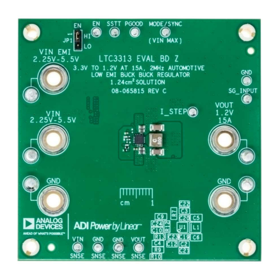
EVALUATION BOARD PHOTOGRAPH
Figure 1. EVAL-LTC3313EV-A-Z Board Photograph
The LTC3313 data sheet gives a complete description of the device
and its application information. The data sheet must be read in
conjunction with this evaluation board user guide. The LTC3313 is
assembled in a 3 mm × 3 mm LQFN package with an exposed
pad for low thermal resistance. The layout recommendations for low
EMI operation and maximum thermal performance are available in
the LTC3313 data sheet.
UG-2077
Rev. 0 | 1 of 11
Advertisement
Table of Contents

Related Manuals for Analog Devices EVAL-LTC3313EV-A-Z


Summary of Contents for Analog Devices EVAL-LTC3313EV-A-Z
-
Page 1: Features
EVAL- LTC3313EV-A-Z with a 3.3 V input in both operation modes. The EVAL-LTC3313EV-A-Z also has an EMI filter to reduce con- ducted EMI. This EMI filter can be included by applying the input voltage at the V EMI terminal. -
Page 2: Table Of Contents
User Guide EVAL-LTC3313 TABLE OF CONTENTS Features..............1 Introduction to the EVAL-LTC3313EV-A-Z..4 Evaluation Kit Contents......... 1 Quick Start Procedure........... 5 Documents Needed..........1 Typical Performance Characteristics..... 6 Equipment Needed..........1 Test Setup..............7 Evaluation Board Photograph........1 EMI Test Results............8 General Description..........1 Evaluation Board Schematic......... 9 Performance Summary..........3... -
Page 3: Performance Summary
User Guide EVAL-LTC3313 PERFORMANCE SUMMARY = 25°C. Table 1. Performance Summary Parameter Test Conditions/Comments Unit 2.25 IN EMI 1.176 1.200 1.224 Output Current, I Efficiency = 3.3 V, I = 5 A 92.5 analog.com Rev. 0 | 3 of 11... -
Page 4: Evaluation Board Hardware
V OUT SW MAX V IN MAX × t ON MIN INTRODUCTION TO THE EVAL-LTC3313EV-A-Z The EVAL-LTC3313EV-A-Z evaluation board features the LTC3313, Select an operating switching frequency below f . It is de- a low voltage, synchronous step-down Silent Switcher. The... -
Page 5: Quick Start Procedure
10. Increase the load by 1 A intervals up to 15 A and observe the voltage output regulation, ripple voltage, and the voltage on the 16. When done, turn off SG_INPUT, PS1, and the load, and remove SSTT turret. all the connections to the EVAL-LTC3313EV-A-Z. °C = − 273 V SSTT 11. -
Page 6: Typical Performance Characteristics
User Guide EVAL-LTC3313 TYPICAL PERFORMANCE CHARACTERISTICS Figure 5. Load Step Response Figure 3. Start-Up Waveforms with Light Load (I Is the Load Inductance.) LOAD Figure 4. Efficiency vs. Load Current analog.com Rev. 0 | 6 of 11... -
Page 7: Test Setup
EVAL-LTC3313 TEST SETUP Figure 6. Test Setup for EVAL-LTC3313EV-A-Z Figure 7. Technique for Measuring Output Ripple and Step Response with a Scope Probe Figure 8. Technique for Measuring Output Ripple and Step Response with a Low Inductance Connector (Not Supplied) analog.com... -
Page 8: Emi Test Results
User Guide EVAL-LTC3313 EMI TEST RESULTS Figure 9. EVAL-LTC3313EV-A-Z CISPR25 Conducted Emission with Class 5 Figure 11. EVAL-LTC3313EV-A-Z CISPR25 Radiated Emission (Vertical) Peak Limits (Voltage Method) Figure 10. EVAL-LTC3313EV-A-Z CISPR25 Radiated Emission (Horizontal) analog.com Rev. 0 | 8 of 11... -
Page 9: Evaluation Board Schematic
User Guide EVAL-LTC3313 EVALUATION BOARD SCHEMATIC Figure 12. EVAL-LTC3313EV-A-Z Evaluation Board Schematic analog.com Rev. 0 | 9 of 11... -
Page 10: Ordering Information
100 kΩ resistor, SMD, 1%, 1/10 W, 0402, AEC-Q200 Panasonic, ERJ-2RKF1003X 4.99 kΩ resistor, SMD, 1%, 1/10 W, 0402, AEC-Q200 Panasonic, ERJ-2RKF4991X 5 V, 15 A, synchronous step-down Silent Switcher in Analog Devices, Inc., LTC3313EV#PBF 3 mm x 3 mm LQFN Additional C1, C18 470 μF tantalum capacitors, 6.3 V, 20%, 7343-40,... - Page 11 Evaluation Board until you have read and agreed to the Agreement. Your use of the Evaluation Board shall signify your acceptance of the Agreement. This Agreement is made by and between you (“Customer”) and Analog Devices, Inc. (“ADI”), with its principal place of business at Subject to the terms and conditions of the Agreement, ADI hereby grants to Customer a free, limited, personal, temporary, non-exclusive, non-sublicensable, non-transferable license to use the Evaluation Board FOR EVALUATION PURPOSES ONLY.
Need help?
Do you have a question about the EVAL-LTC3313EV-A-Z and is the answer not in the manual?
Questions and answers