Table of Contents
Advertisement
Quick Links
Advertisement
Table of Contents

Related Manuals for NXP Semiconductors PN7160


Summary of Contents for NXP Semiconductors PN7160
- Page 1 UM11496 PN7160 evaluation board Rev. 1.3 — 24 November 2022 User manual Document information Information Content Keywords OM27160, PN7160, PN7161, evaluation kit Abstract This document is the user manual of the PN7160/PN7161 evaluation board.
-
Page 2: Revision History
UM11496 NXP Semiconductors PN7160 evaluation board Revision history Revision history Date Description 20221124 • Section 2 "Introduction": IMPORTANT NOTICE added • Section 7 "Radio Equipment Directive (RED)": added • Table 5: updated the terms "Master/Slave" to "Controller/Target" and "MOSI/MISO" to "COTI/CITO"... -
Page 3: Introduction
The present document describes the OM27160 evaluation board, a flexible and easy-to- use NFC controller board featuring PN7160. It enables the development of an NFC solution based on PN7160 in a Linux or Android environment or even in system based on RTOS or without OS. -
Page 4: Om27160 Board Overview
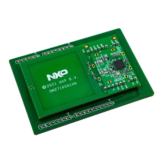
UM11496 NXP Semiconductors PN7160 evaluation board OM27160 board overview The OM27160 board is high performance fully NFC-compliant expansion board, meeting compliance with reader mode, P2P mode and card emulation mode standards. The board features an integrated high performance 40 mm * 40 mm RF antenna to insure high interoperability level with NFC devices. -
Page 5: Om27160 Board Details
UM11496 NXP Semiconductors PN7160 evaluation board OM27160 board details 4.1 Schematics Figure 2. OM27160A1HN board schematics UM11496 All information provided in this document is subject to legal disclaimers. © 2022 NXP B.V. All rights reserved. User manual Rev. 1.3 — 24 November 2022... - Page 6 UM11496 NXP Semiconductors PN7160 evaluation board Figure 3. OM27160B1HN board schematics UM11496 All information provided in this document is subject to legal disclaimers. © 2022 NXP B.V. All rights reserved. User manual Rev. 1.3 — 24 November 2022 6 / 19...
-
Page 7: Layout
UM11496 NXP Semiconductors PN7160 evaluation board 4.2 Layout 4.2.1 Components layers Figure 4. OM27160 board components layers 4.2.2 Layer 1 Figure 5. OM27160 board layer 1 UM11496 All information provided in this document is subject to legal disclaimers. © 2022 NXP B.V. All rights reserved. -
Page 8: Layer 2
UM11496 NXP Semiconductors PN7160 evaluation board 4.2.3 Layer 2 Figure 6. OM27160 board layer 2 4.2.4 Layer 3 Figure 7. OM27160 board layer 3 UM11496 All information provided in this document is subject to legal disclaimers. © 2022 NXP B.V. All rights reserved. -
Page 9: Layer 4
UM11496 NXP Semiconductors PN7160 evaluation board 4.2.5 Layer 4 Figure 8. OM27160 board layer 4 UM11496 All information provided in this document is subject to legal disclaimers. © 2022 NXP B.V. All rights reserved. User manual Rev. 1.3 — 24 November 2022... -
Page 10: Additional Information
5.1 Using different I C address The OM27160A1HN board come with default 0x28 (7 bits) I C PN7160 slave address. However, it is still possible to change it (between 0x28 and 0x2B) by setting of R10, R11, R12 and R13 resistors. - Page 11 UM11496 NXP Semiconductors PN7160 evaluation board Figure 10. OM27160 board interface connectors Table 2. OM27160 board J1 connector pinout PN7160 signal VDD(PAD): 1.8 V or 3.3 V host interface voltage reference VDD(UP/VBAT: 2.8 V to 5.5 V supply voltage Table 3. OM27160 board J2 connector pinout (only relevant for OM27160A1HN...
- Page 12 UM11496 NXP Semiconductors PN7160 evaluation board Table 4. OM27160 board J3 connector pinout ...continued PN7160 signal Not connected Table 5. OM27160 board J4 connector pinout (only relevant for OM27160B1HN version) PN7160 signal SPI_COTI: SPI-bus Controller Output, Target Input data SPI_CITO: SPI-bus Controller Input, Target Output data...
-
Page 13: References
PN7160 evaluation board References The OM29110 Interface boards are used to connect NFC’s demo boards (e.g. OM5579 related to PN7150 NFC controller or OM27160 related to PN7160 NFC controller) to Single-Board-Computer (like Raspberry Pi, BeagleBone, or board featuring Arduino header). -
Page 14: Radio Equipment Directive (Red)
UM11496 NXP Semiconductors PN7160 evaluation board Radio Equipment Directive (RED) The following information is provided per Article 10.8 of the Radio Equipment Directive 2014/53/EU: (a) Frequency bands in which the equipment operates. (b) The maximum RF power transmitted. Table 6. Characteristics... -
Page 15: Legal Information
NXP Semiconductors. In no event shall NXP Semiconductors, its affiliates or their suppliers In no event shall NXP Semiconductors be liable for any indirect, incidental, be liable to customer for any special, indirect, consequential, punitive punitive, special or consequential damages (including - without limitation -... - Page 16 Purchase of NXP Semiconductors IC does not include a and trade secrets. All rights reserved.
- Page 17 UM11496 NXP Semiconductors PN7160 evaluation board Tables Tab. 1. I2C address configuration ....... 10 Tab. 4. OM27160 board J3 connector pinout ....11 Tab. 2. OM27160 board J1 connector pinout ....11 Tab. 5. OM27160 board J4 connector pinout (only Tab.
- Page 18 UM11496 NXP Semiconductors PN7160 evaluation board Figures Fig. 1. OM27160 board overview ......... 4 Fig. 7. OM27160 board layer 3 ........8 Fig. 2. OM27160A1HN board schematics ....5 Fig. 8. OM27160 board layer 4 ........9 Fig. 3. OM27160B1HN board schematics ....6 Fig.
-
Page 19: Table Of Contents
UM11496 NXP Semiconductors PN7160 evaluation board Contents Revision history ..........2 Introduction ............3 OM27160 board overview ........4 OM27160 board details ........5 Schematics ............5 Layout ..............7 4.2.1 Components layers ..........7 4.2.2 Layer 1 .............. 7 4.2.3 Layer 2 .............. 8 4.2.4...
Need help?
Do you have a question about the PN7160 and is the answer not in the manual?
Questions and answers