Advertisement
Quick Links
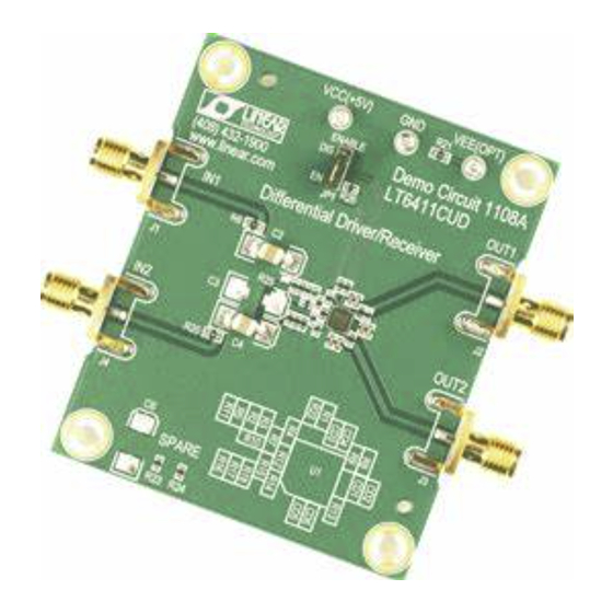
DESCRIPTION
Demonstration circuit 1057 is a reference design
featuring Linear Technology Corporation's LT6411
High Speed Amplifier/ADC Driver with an on-board
LTC2249 14-bit, 80MSPS ADC. DC1057 demon-
strates good circuit layout techniques and recom-
mended component selection for optimal system
performance. The ADC driver input and output
networks are flexible, allowing for AC or DC cou-
pling, gains of 0dB or 6dB, single-ended or differ-
ential configurations, and signal low-pass or band-
pass filtering before the ADC.
QUICK START PROCEDURE
Validating the performance of the LT6411 ADC
Driver-ADC combination is simple with DC1057,
and requires only two signal generators and some
basic lab equipment. Table 1 shows the function of
each I/O connector and selectable jumper on the
board. Refer to Figure 1 for proper board evalua-
tion equipment setup and follow the procedure be-
low:
1. Connect the power supplies as shown. The
power supply connector labeled VCC powers
the ADC driver. VDD powers the ADC, and
OVDD provides power to both the ADC output
stage and the two CMOS output buffers. The
entire board and all components share common
ground planes. Check the supply voltages be-
fore applying power, to avoid damage from over-
voltage conditions.
2. Provide an encode clock to the ADC via SMA
connector J4. For best performance, a high-
quality sine wave synthesizer with an external
band-pass filter will provide a stable, low-phase-
noise clock source. A crystal oscillator will also
provide good performance. DC1057 includes an
DEMO CIRCUIT 1057
LT6411 AND LTC2249 ADC
QUICK START GUIDE
LT6411 High-Speed
ADC Driver Combo
DC1057 also allows the flexibility of selecting the
CMOS output supply voltage. DC1057 includes an
on-board 40-pin edge connector for use with the
DC718 Data Acquisition demo board and Linear
Technology's QuickEval-II data processing soft-
ware,
available
http://www.linear.com.
Design files for this circuit board are available.
Call the LTC factory.
, LTC and LT are registered trademarks of Linear Technology Corporation.
on-board clock amplifier/buffer IC to provide a
large-amplitude clock source to the ADC.
NOTE. A poor quality encode clock can significantly degrade the
signal-to-noise ratio (SNR) of the driver-ADC combination.
Table 1: DC1057 Connectors and Descriptions
REFERENCE
FUNCTION
Analog Input (50Ω termination imped-
J1 (AIN+)
ance)
Analog Input (by default, tied to ground
J2 (AIN-)
via resistor R16 for single-ended-to-
differential conversion)
J3 (40-pin conn)
Provides direct connection to DC718.
CMOS Output Buffers provide parallel
data output and clock signals (see sche-
matic)
J4 (Encode
ADC Encode Clock. For best perform-
Clock)
ance, use a high-quality low-jitter clock
source.
JP1 (ENABLE)
Enable/Disable LT6411. Default is EN.
3. Apply an input signal to the board. DC1057 al-
lows great flexibility in applying input signals
(see the section on Applying Input Signals). For
best results, use a low distortion, low noise sig-
nal generator with high order low-pass or band-
Board
on
our
website
at
1
Advertisement

Related Manuals for Linear Technology LT6411


Summary of Contents for Linear Technology LT6411
- Page 1 0dB or 6dB, single-ended or differ- Call the LTC factory. ential configurations, and signal low-pass or band- , LTC and LT are registered trademarks of Linear Technology Corporation. pass filtering before the ADC. QUICK START PROCEDURE Validating the performance of the LT6411 ADC...
- Page 2 LT6411 AND LTC2249 ADC pass filtering to avoid degrading the perform- ing software. See Figure 2 for the general board ance of the ADC driver and ADC. evaluation setup diagram. 4. Observe the ADC output with demo circuit NOTE. See the DC718 Quick Start Guide for instructions on using the DC718 QuickDAACS data acquisition demo board.
-
Page 3: Additional Information
R17, R18 resistors. (Figure 4a) formance differential input drive (or transformer- Install 0Ω at R5, R10. coupled drive) is recommended. By default, trans- former drive is used on DC1057 so that only a sin- gle-ended input is needed. See the LT6411 data-... - Page 4 The output common-mode voltage of the ADC (Figure 4d) Establish DC bias by using R2/R3 and driver must be set either at the input of the LT6411 R17/R18. (see Table 2), or by AC coupling the output of the Install 0Ω at R40, R41 to establish gain of - LT6411.
- Page 5 LT6411 HIGH-SPEED ADC DRIVER COMBO BOARD toolbar, select DC718 (QuickDAACs). The next if the output randomizer is turned on (via JP4). Af- step is to use the proper settings for the DC1057 ter configuration is through, the program should be output.
- Page 6 LT6411 HIGH-SPEED ADC DRIVER COMBO BOARD Figure 4. Pictures of DC1057 input network configurations. Blocks show where components should be mounted, ac- cording to Table 2.
- Page 7 LT6411 HIGH-SPEED ADC DRIVER COMBO BOARD Figure 5. Selecting the correct input to QuickEval-II Figure 6. Entering the correct device information for your ADC. Select the correct device for your board.
- Page 8 LT6411 HIGH-SPEED ADC DRIVER COMBO BOARD...
- Page 9 LT6411 HIGH-SPEED ADC DRIVER COMBO BOARD...
- Page 10 Mouser Electronics Authorized Distributor Click to View Pricing, Inventory, Delivery & Lifecycle Information: Analog Devices Inc. DC1057A...
Need help?
Do you have a question about the LT6411 and is the answer not in the manual?
Questions and answers