Table of Contents
Advertisement
Quick Links
FEATURES
Single-ended and differential input capability
Multiple input interface connection options (jack or header)
Optimized EMI suppression filter assembled on board
PCB footprint for dc power supply jack (accepts 2.5 V to 5.5 V)
GENERAL DESCRIPTION
The SSM2311 is a fully integrated, single-chip, mono Class-D
audio amplifier. It is designed to maximize performance for
mobile phone applications. The application circuit requires a
minimum of external components and operates from a single
2.5 V to 5.5 V supply. It is capable of delivering 3 W of conti-
nuous output power with less than 1% THD + N driving an
3 Ω load from a single 5.0 V supply.
The SSM2311 comes with a differential mode input port and a
high efficiency H-bridge at the output. When compared to a half-
bridge output stage, a full H-bridge enables direct coupling of
the audio power signal to the loudspeaker, doubling the output
voltage swing and eliminating the need for a large output
coupling capacitor. Another benefit of a full H-bridge is an
increase of the maximum output power by 4× when compared
to a half bridge under the same load impedance. These benefits
are particularly useful for low voltage, battery-powered
portable electronics where energy and space are limited. The
differential mode input stage
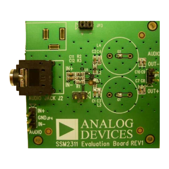
Figure 1. SSM2311 Evaluation Board Top View
Rev. 0
Evaluation boards are only intended for device evaluation and not for production purposes.
Evaluation boards are supplied "as is" and without warranties of any kind, express, implied, or
statutory including, but not limited to, any implied warranty of merchantability or fitness for a
particular purpose. No license is granted by implication or otherwise under any patents or other
intellectual property by application or use of evaluation boards. Information furnished by Analog
Devices is believed to be accurate and reliable. However, no responsibility is assumed by Analog
Devices for its use, nor for any infringements of patents or other rights of third parties that may
result from its use. Analog Devices reserves the right to change devices or specifications at any
time without notice. Trademarks and registered trademarks are the property of their respective
owners. Evaluation boards are not authorized to be used in life support devices or systems.
Filterless Class-D Audio Amplifier
allows for cancelling of common-mode noise leading to a
superior CMRR.
Moreover, the part features a high efficiency, low noise output
modulation scheme that does not require external LC output
filters when attached to an inductive load. The modulation
provides high efficiency even at low output power. Filterless
operation also helps to decrease distortion due to nonlinearities
of output LC filters, thereby providing a better sound quality
and leading to savings in board space and overall cost.
This data sheet describes how to configure and use the SSM2311
evaluation board. It is recommended that this data sheet be
read in conjunction with the SSM2311 data sheet, which
provides more detailed information about the specifications,
internal block diagrams, and application guidance for the
amplifier IC.
EVALUATION BOARD DESCRIPTION
The SSM2311 evaluation board carries a complete application
circuit for driving a loudspeaker. Figure 1 shows the top view
of the evaluation board and Figure 2 shows the bottom view.
The top layer with its silkscreen of the evaluation board is shown
in Figure 5. Figure 6 and Figure 7 show the top silkscreen and
bottom silkscreen, respectively. The top layer, Layer 2 (ground
plane), Layer 3 (power plane), and bottom layer are shown in
Figure 8, Figure 9, Figure 10, and Figure 11, respectively.
Figure 2. SSM2311 Evaluation Board Bottom View
One Technology Way, P.O. Box 9106, Norwood, MA 02062-9106, U.S.A.
Tel: 781.329.4700
Fax: 781.461.3113
Evaluation Board for
EVAL-SSM2311
©2008 Analog Devices, Inc. All rights reserved.
www.analog.com
Advertisement
Table of Contents

Subscribe to Our Youtube Channel
Related Manuals for Analog Devices EVAL-SSM2311


Summary of Contents for Analog Devices EVAL-SSM2311
-
Page 1: Features
Devices for its use, nor for any infringements of patents or other rights of third parties that may One Technology Way, P.O. Box 9106, Norwood, MA 02062-9106, U.S.A. result from its use. Analog Devices reserves the right to change devices or specifications at any Tel: 781.329.4700 www.analog.com... -
Page 2: Table Of Contents
EVAL-SSM2311 TABLE OF CONTENTS Features ....................1 What to Test ...................3 General Description ................. 1 Component Selections ..............3 Evaluation Board Description ............1 PCB Layout Guidelines ..............5 Revision History ................2 Evaluation Board Schematic and Artwork ........6 ... -
Page 3: Evaluation Board Hardware
EVAL-SSM2311 EVALUATION BOARD HARDWARE POWER SUPPLY EMI filter should be removed. Short across the ferrite bead terminals and open the capacitor terminals. The schematic is shown in Figure 4. GETTING STARTED On the upper left corner, there is a PCB footprint to populate a standard power jack (J1), which accepts a 2.5 V ~ 5.5 V dc... - Page 4 EVAL-SSM2311 tance (DCR) of these beads, the better for minimizing their Output Inductors—L3 and L4 power consumption. Table 1 describes the recommended bead. Some users do not allow high frequency EMIs in the system and prefer using inductors to filter out the high frequency components Output Shunting Capacitors at the output nodes.
-
Page 5: Pcb Layout Guidelines
EVAL-SSM2311 Layer Stacks and Grounding PCB LAYOUT GUIDELINES The stack-up for the evaluation board is a 4-layer structure. To keep the EMI under the allowable limit and to ensure that the amplifier chip operates under the temperature limit, PCB Top layer—component layer with power and output copper... -
Page 6: Evaluation Board Schematic And Artwork
EVAL-SSM2311 EVALUATION BOARD SCHEMATIC AND ARTWORK 15µH 0.1µF 10µF IN– HDR1X3 B0603 OUT+ OUT+ 0.1µF 0Ω 100pF 100pF HDR1X2 B0603 OUT– IN– 0.1µF OUT– 0Ω SSM2311 100pF 100pF 15µH 100kΩ HDR1X2 PWRJACK_PJ002A NOTES 1. L3, L4, C7, C8, C9, C10, AND J1 ARE NOT POPULATED. - Page 7 EVAL-SSM2311 Figure 5. Top Layer with Top Silkscreen Figure 7. Bottom Silkscreen Figure 6. Top Silkscreen Figure 8. Top Layer Rev. 0 | Page 7 of 12...
- Page 8 EVAL-SSM2311 Figure 11. Bottom Layer Figure 9. Layer 2 (Ground Plane) Figure 10. Layer 3 (Power Plane) Rev. 0 | Page 8 of 12...
-
Page 9: Ordering Information
15 μH Not populated 100 kΩ resistor, 1/10 W, 1% Digi-Key 311-100KHRCT-ND R2, R3 0 Ω resistor, 1/10 W, 5% Digi-Key 311-0.0GRCT-ND SSM2311 Analog Devices SSM2311 ORDERING GUIDE ESD CAUTION Model Description SSM2311-EVALZ Evaluation Board Z = RoHS Compliant Part. - Page 10 EVAL-SSM2311 NOTES Rev. 0 | Page 10 of 12...
- Page 11 EVAL-SSM2311 NOTES Rev. 0 | Page 11 of 12...
- Page 12 EVAL-SSM2311 NOTES ©2008 Analog Devices, Inc. All rights reserved. Trademarks and registered trademarks are the property of their respective owners. EB07658-0-9/08(0) Rev. 0 | Page 12 of 12...
Need help?
Do you have a question about the EVAL-SSM2311 and is the answer not in the manual?
Questions and answers