Table of Contents
Advertisement
Advertisement
Table of Contents

Related Manuals for JBL LSR28P


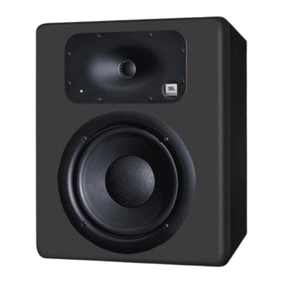
Summary of Contents for JBL LSR28P
- Page 1 Technical Service Manual Rev. A 3/14/2003...
-
Page 2: Table Of Contents
TABLE OF CONTENTS PRODUCT OVERVIEW OVERALL FREQUENCY RESPONSE SERVICING NOTES AND DISCLAIMERS SPECIFICATIONS THE JBL LIMITED WARRANTY TOOLS NECESSARY FOR SERVICE SERVICE PROTOCOLS 10-11 A WORD ABOUT BALANCED AND UNBALANCED INPUTS CONNECTOR WIRING/TYPICAL BENCH SETUP 13-14 SELECTIBLE INPUT SENSITIVITY BLOCK DIAGRAM... -
Page 3: Product Overview
What this means to the user is that the LSR28P will exhibit consistent performance at low, medium and high levels of volume during the entire musical session. -
Page 4: Overallfrequency Response
OVERALLFREQUENCY RESPONSE The frequency response of the output from the crossover system is shown in the figure below. AUDIO PRECISION LEVEL(dBu) & 2-CHAN(dBu) FREQ(Hz) Crossover Response 10.000 5.0000 -5.000 -10.00 -15.00 -20.00 -25.00 -30.00 When a system under test shows a different result in the frequency response test, as shown above, using a +4dBu input signal to the XLR connector with no DIP switches selected, the source of the error can be investigated by referring to the following sections located within the troubleshooting guide. -
Page 5: Servicing Notes And Disclaimers
SAFETY PRECAUTION STATEMENT There are no user servicible parts inside! Attempting to repair this product or opening the cabinet will expose the user to hazardous high voltage. Servicing and repair should be referred to authorized technical personnel only. - Page 6 LIABILITY WAIVER JBL PROFESSIONAL IS NOT LIABLE FOR ANY DIRECT OR INDIRECT DAMAGE TO THIS OR ANY ASSOCIATED PROPERTY ARISING FROM THE USAGE OR THE INABILITY TO USE THIS PRODUCT.
-
Page 7: Specifications
Signal Input: XLR Balanced with pin 2 Hot @ 120k Ohm impedance SYSTEM COMPONENTS Cabinet Resonance Frequency: 38 Hz Low Frequency Transducer JBL #(218F) 203mm (8 in.) Cone DC Resistance: 1.8-ohm ± 10% Differential Drive, Dynamic Braking High Frequency Transducer: JBL# (053Ti) DC Resistance: 3.5 ohm - 3.8 ohm... -
Page 8: The Jbl Limited Warranty
WARRANTY INFORMATION All JBL LSR products carry the transferable, JBL Professional Limited Warranty covering all defects in material and workmanship for a full five years from the original date of purchase. Electronic components and circuitry is warranted for three years. For more specific information, consult the warranty card that is packed with the product. -
Page 9: Tools Necessary For Service
ESSENTIAL TOOLS In order to successfully service and maintain this speaker system, the technician should have, at a minimum, the following test instruments. Oscilloscope, at least 20 MHz bandwidth Digital Multimeter, with a minimum of 50kohm Impedance for various troubleshooting Line Voltage Variac with Ammeter for measuring proper voltage/ current consumption. -
Page 10: Service Protocols
SERVICE PROTOCOLS The maintenance of an electronic system can be divided into many sequential processes that have to be explicitly followed in order to achieve a final result. Partial repair or incomplete repair will not suffice for the professional technician intent on complete customer satisfaction and will not adequately restore proper operation to a malfuntioning unit. - Page 11 listener to hear the input media more accurately albeit at the expense of a more difficult and time consuming troubleshooting analysis. Most of the repairs that are necessary to the LSR monitor system can be traced either to the PCB connections at the component legs to an actual failure of the electromechanical components .
-
Page 12: A Word About Balanced And Unbalanced Inputs
So, it is of critical importance that the Audio System be correctly installed. There are three methods of connecting the source output to the source input of the LSR28P System. Each method has its own attributes and the NUETRIK Combo connector can accommodate all methods of hookup, however, the quietist and most universally accepted method of hookup for the professional environment is the first method or “balanced input.”... -
Page 13: Connector Wiring/Typical Bench Setup
BALANCED AND UNBALANCED CONNECTIONS SUGGESTED INSTRUMENT SETUP O’SCOPE INPUT DISTORTION OUTPT METER ANALYZER CHNL CHNL METER SIGNAL GENERATOR 4 Ω LOAD UNIT UNDER VOLT/OHM VARIAC TEST ISOLATION WITH METER XSFRMR CURRENT METER... - Page 14 The third method of connecting signal to the LSR28P is still an unbalanced hookup and is a variation of the above XLR method by using a two-conductor cable or RCA cable with two XLR adapters at each end or two Tip/Ring/Sleeve connectors at each end.
-
Page 15: Selectible Input Sensitivity
4,8, or 12 dB of signal attenuation can be inserted in the input line by using the DIP switches on the back of the LSR28P. See the illustration below: Located on the right of the Neutrik connector but before the power switch, is a bank of switches that are accessible with the use of a pen or a very small screwdriver. -
Page 16: Block Diagram
BLOCK DIAGRAM LSR28P Signal PreAmp PWR. AMP TRIM Speaker DIP Switch TRIM Gain Speaker Trim PWR. AMP PreAmp... -
Page 17: Theory And Circuit Descriptions
THEORY AND CIRCUIT DESCRIPTIONS... -
Page 18: Power Supply
POWER SUPPLY Initially, raw alternating current enters the LSR28P from the IEC connector on the signal input processing board and is directly connected to the power switch S3 through the main fuse F1. . From there, it travels to the voltage selector switch that determines which primary on the transformer connected. -
Page 19: Input Buffer Amplifier
INPUT BUFFER AMPLIFIER Input = 0 dB/2.2 Vpp @ 100 Hz Output= 1.1 Vpp The integrated circuit, U3, provides several functions. U3A is used as an input buffer amplifier which isolates the source signal from deterioration caused by the user selectable DIP switches, SW1A.,B,AND C. - Page 20 HIGH FREQUENCY PROCESSING Input= 1 Vpp Output= . 8 Vpp The circuit, shown above, is used for the high frequency processing of the input signal. Physically, it is located on the input circuit board. Its purpose is to actively filter out or attenuate the low frequency component from the composite signal leaving only the high frequencies to be contoured by the user and, eventually, sent to power amplifier for final amplification.
-
Page 21: Low Frequency Processing
LOW FREQUENCY PROCESSING Input 1.1 Output=. 95 Vpp This is the processing circuitry for the low frequency spectrum. We are interested in this circuit, shown above, because it provides the signal path that will discriminate the low frequency component from the composite signal and filters that component out by actively rejecting high frequency signals above the high critical frequency. -
Page 22: Final Low Frequency Filter
FINAL LOW FREQUENCY FILTER Ouput= .95 Vpp Input= .95Vpp @ 100 Hz The two-pole active Butterworth low pass filter, shown above, is situated on the main PCB board. Circuit-wise, it is located immediately before entering the main low frequency amplifier. It effectively removes any ultra high frequency noise that might have slipped by the main filtering or been induced in the interface input cabling after the main filtering and attenuates that signal at a rate of -40 dB after the critical frequency. -
Page 23: Low Frequency Output Amplifier
LOW FREQUENCY OUTPUT AMPLIFIER WITH MUTED POWER UP AND THERMAL SHUTDOWN The low frequency amplifier uses discrete components configured in a push-pull drive architecture operating in the class AB region and have a measurable gain of 15.25 dB. The voltage rails for the power amplifier are positive and negative 42 volts as rectified by bridge BR1 located in the Power Supply Module. -
Page 24: High Frequency Output Amplifier
Input = . 8Vpp @ 10KHz Output = 11.8 Vpp The circuit shown above is the high frequency power amplifier used in the LSR28P. It uses an LM3886T operational power amplifier in a non-inverting configuration with the normal peripheral components to provide proper equalization and operation. The nominal operating voltage of positive and negative 36V is applied to the IC via pin 4 and pins 1 and 5, respectively. -
Page 25: Fault Indication Circuitry
FAULT INDICATION CIRCUITRY The detection circuitry for the LSR28P revolves around the quad comparator NJM2901N (U3). There are a number of individual faults monitored for including voltage offset on both the low and high frequency amplifiers, excessive current usage by the unit, and an over-limit input signal level resulting in clipping. -
Page 26: Troubleshooting Guide
• If product is out of warranty, contact the customer with an estimate of the repair charges. Note: It is the policy of JBL Professional to always give the customer "the benefit of doubt" concerning decisions of eligibility of warranty coverage. This not only is a good business practice in the long run but also promotes customer good faith and satisfaction. - Page 27 The majority of problems in use will be with electro-mechanical components; DIP Switches SW1, switches SW2 and SW3, potentiometers R1, R4 and R56. Before dis-assembling a faulty LSR28P system check the action of these electro-mechanical elements as follows: • System Fails to Power Up 1.
- Page 28 B) Power Supply Test Verify that +15V and -15V supplies are at the correct levels. C) Power Switching Test Use an ohmmeter or continuity tester to ensure that both the power switch SW3 and line voltage selector switch SW2 operate correctly by metering between IEC connector S1 active pin and connector P2 pins 2 and 4 and between IEC connector S1 neutral pin and connector P2 pins 1 and 3 with the voltage selector SW2 at 115V.
- Page 29 OVERALL FREQUENCY RESPONSE The response of both outputs from this crossover system are shown in the figure below. AU D IO P R E C ISIO N LEVEL(dBu) 2-CHAN(dBu) FREQ (Hz) Crossover Response & 10.000 5.0000 -5.000 -10.00 -15.00 -20.00 -25.00 -30.00 Where the system under test shows a different result in a frequency response test using a +4dBu...
- Page 30 Low Frequency Signal Path Gain The curves in the figure below plot the frequency response from a +4dBu input signal at the outputs of U2 pin 1, U5 pin 7, U6 pin 7 and U7 pin 1. U2A acts as a second order low pass filter as shown by the top curve. U5A and B form a bell equalization cut centered on about 600Hz.
- Page 31 • The curve with a boost centered around 35Hz is the result of selecting the +2dB bass boost switch SW1F. If this curve is not obtained but other responses are correct change Q1. • The curve with a drooping response below 80Hz is the result of selecting the -2dB bass cut switch SW1E.
- Page 32 HIGH FREQUENCY SIGNAL PATH GAIN The curves in the figure below, which are taken with trimmer R4 at minimum (fully ccw) plot the frequency response from a +4dBu input signal at the outputs of U1 pin 1, U1 pin 7 and U4 pin 1.
- Page 33 RESPONSE CURVES DEPICTING DIP SWITCH SELECTION DIP switches SW1G and H adjust the gain of the stage around U4A. The effect of selecting these switches is shown in the curves at the figure below. The highest gain curve is the result of selecting SW1H whereas the lowest gain curve is the result of selecting SW1G.
- Page 34 TROUBLESHOOTING MAIN AMPLIFIER Setup: The quickest and most efficient way to operate the LSR28P Main amplifier board is to use a known, good LSR28P input PCB. Connect the boards together using an 8-pin connecting cable assembly. Attach the secondary of the main power transformer (JBL# 562-00032-00) to J6 on the main amplifier and the primary to P2 on the input PCB.
- Page 35 The amplifier will begin to clip at around 55 V P/P. If the amp prematurely clips, verify that the input signal is not clipped. This can be measured at the junction of R48 and C23. Upon reaching the 50 V P/P clipping plateau at the amp output, there should be around 3.2V P/P at the input to the amp.
- Page 36 MAIN VOLTAGE TESTS +/- 15V Supply Test Slowly ramp up the Variac, never allowing the supplies to exceed +/-16V. Measure + 15V and -15V supplies at Q2 and Q4. Both should be the correct value +/-15V, respectively. If a supply is very close to the ground potential (Less than +/- 100mV) check for shorts on the +/- 15V supplies lines.
- Page 37 shorted SW1; To verify correct operation, interrupt power while monitoring collector of Q17. The voltage should quickly change to + 15 and, eventually, zero volts. If it does not, check for open C29 and, or Q17; With negative voltage applied to pin 6 of U1B, pin 7 of U1B should be at +15V. If not, check for short or open trace around pins 5 and 6 or replace the defective IC U1.
- Page 38 Crossover Distortion in Output Figure A Output Waveform Crossover Distortion Distortion Waveform Refer to Figure A above and note the character of crossover distortion. This is caused by both halves of the output stage (Q6, Q7 on positive side, and Q8 , Q9 on the negative side) being turned off right around crossover (crossover from positive drive to negative drive).
- Page 39 Excessive Second harmonic distortion in output Figure B Output Waveform Distortion Waveform (Second Harmonic) Refer to Figure B above and note the character of second harmonic distortion. This is caused by an imbalance in amplifying capability in either the current amplifier or the voltage amplifier. Note that the “Distortion Waveform”...
- Page 40 Check all components that affect high frequency stability and response; C11, R27 (output loading), C2, C5 (Current amp stabilizers), C30, R31 and C32. • Is there crossover distortion in the output? To verify this note the character of crossover distortion. This is caused by both halves of the output stage (Q6, Q7 on positive side, and Q8, Q9 on the negative side) being turned off right around crossover (crossover from positive drive to negative drive).
- Page 41 If all of this is okay replace Bias Set Procedure The following steps are necessary to set the bias on the LSR28P low frequency amplifier module, PCB 510-00032-XX rev (any).
- Page 42 Voltage Amplifier Test. Turn the signal generator off. Disconnect 2-ohm load. Lift one side of R44. Connect base of Q16 to base of Q18. Power up amplifier. Verify that the voltage at U1B pin 7 is around +15 volts. If not, refer to “Amplifier Muting Test.”...
- Page 43 4. Lower Class A drive Verify that voltage across R21 equals 870mV +/- 20%. If incorrect, check Q13 for open or shorted elements. Check the voltage at the base of Q11. This should be half way between the negative supply voltage and the output node.
- Page 44 Low Frequency Filter Test Turn on generator output A, adjust frequency for 900Hz, and adjust oscillator level to obtain 3V P/P at the input to the filter, pin 1 of J3. Move probe to junction of R48 and C23. The curve on the graph shown above represents the transfer function in dB of the first filter section at U1A when this section is operating properly.
- Page 45 High Frequency Power Amplifier Test • HF Amplifier pulls excessive current when board is powered up If the output of the amplifier, pin 3 of U2, is centered (around ground potential) check for a short from ground to the output pin, pin 3 of U2. If no shorting problem is found replace U2.
- Page 46 • Does amp oscillate? Verify correct values of C35, C25, C28, and C36. Is there an oscillation on the rails that is not being filtered? If all this is okay and gain test above has been passed, replace U2 • Is output distorted? Verify pin 8 of U2 measures approximately -3volts.
- Page 47 Verify around 5 volts at U3 pin 8. If not, replace U3. Check continuity from U3 pin 14 to J7 pin 1. If correct, replace U3. Apply an input signal at 500Hz sufficient to produce 50 volts peak to peak at the low frequency amplifier output and observe that the red LED illuminates.
-
Page 48: Final Test Procedures
FINAL TEST PROCEDURES For the final test of the LSR28P, the following check out procedures can be followed. If the technician measures radically different values for the individual tests, the amplifier should be troubleshot and repaired to conform to factory specifications. -
Page 49: Exploded Views And Graphics
Click here to view component exploded view http://www.jblproservice.com/pdf/LSR%20Series/LSR28P.pdf... - Page 50 LSR28P COMPONENT EXPLODED VIEW COMPONENT PARTS LIST Item Part No. Qty. Description Ref. Des. Item Part No. Qty. Description Ref. Des. 684-00003-00 3 IC,NJM4560D U2,U5,U6,U7 546-00005-00 SW, Voltage Selector 660-00027-01 1 RES.TRIM POT 5K 660-00027-00 RES,TRM POT 500 684-00000-00 3 IC,NJM2068D...
- Page 51 LSR28P COMPONENT EXPLODED VIEW COMPONENT PARTS LIST Item Part No. Qty. Description Ref. Des. Item Part No. Qty. Description Ref. Des. RR6,R8,R23,R2 682-00011-00 XSTR,NPN, 2SC3281 Q6,Q7 632-71008-50 4 RES.10 OHM 5% 3W 682-00006-00 XSTR, NPN, 2SD1763A Q1,Q2,Q3 604-06109-60 2 CAP,10,000 UF, 63V...
-
Page 52: Wiring Diagram
Wiring Diagram LSR28P... -
Page 53: Semiconductor Pinouts
SEMICONDUCTOR PINOUTS... -
Page 54: Pcb Pictorials
LSR28P PICTORIAL OF COMPLETE AMPLIFIER ASSEMBLY COMPONENT PARTS LIST Item Part No. Qty. Description 124-58002-00x Speaker low freq. 218F 123-10003-00X Speaker H F M/I 053TI 226-00013-00 Main Amp Assy W/Heatsink 226-00012-00 Signal Input Assy 562-00032-00 Transformer... - Page 55 LSR28P PICTORIAL OF INTERFACE PCB ASSEMBLY COMPONENT PARTS LIST Item Part No. Qty. Description 513-00034-01 Interface Cable Assembly...
- Page 56 LSR28P PICTORIAL OF INPUT PCB ASSY COMPONENT PARTS LIST Item Part No. Qty. Description Ref.Des. Item Part No. Qty. Description Ref.Des. 684-00003-00 IC,NJM4560D U2,U5,U6,U7 546-00005-00 SW, Voltage Selector 660-00027-01 RES.TRIM POT 5K 660-00027-00 RES,TRM POT 500 684-00000-00 IC,NJM2068D U1,U4,U8 548-00018-01...
- Page 57 LSR28P COMPONENT EXPLODED VIEW COMPONENT PARTS LIST Item Part No. Qty. Description Ref.Des. Item Part No. Qty. Description Ref.Des. 682-00011-00 XSTR,NPN, 2SC3281 Q6,Q7 632-71008-50 RES.10 OHM 5% 3W R6,R8,R23,R25 682-00006-00 XSTR, NPN, 2SD1763A Q1,Q2,Q3 604-06109-60 CAP,10,000 UF, 63V C16,C17 548-00015-00...
-
Page 58: Master Parts List
Click here for the Master Parts Listing http://www.jblproservice.com/pdf/LSR%20Series/LSR28P%20AMP%20BOM.pdf Click here to view the JBL Professional Electronic Failure QA Codes http://www.jblproservice.com/protected/Domestic%20pdf/Electronic%20QA%20Codes.pdf Click here for Schematics http://www.jblproservice.com/pdf/LSR%20Series/LSR28P%20Schematics.pdf... -
Page 67: Electronic Failure Qa Codes
Network failures should continue to use the transducer failure codes. Please utilize these codes on every warranty claim submitted to JBL Professional. Exclusion of these codes will result in the return of warranty claims. - Page 68 JBL PROFESSIONAL ELECTRONIC FAILURE Q.A. CODES July 1, 2002 Page 1 Q.A. DESCRIPTION OF DEFECT WARRANTY Q.A. DESCRIPTION OF DEFECT WARRANTY CODE STATUS CODE STATUS 10.010 IC (Specify) 10.058 Capacitor - Value Changed 10.011 IC - Open 10.059 Capacitor - Broken 10.012 IC - Burned *...
- Page 69 JBL PROFESSIONAL ELECTRONIC FAILURE Q.A. CODES July 1, 2002 Page 2 Q.A. DESCRIPTION OF DEFECT WARRANTY Q.A. DESCRIPTION OF DEFECT WARRANTY CODE STATUS CODE STATUS 10.192 Cables - Noisy 10.130 CONNECTOR (Specify) 10.131 Connector - Intermittent 10.193 Cables - Cut - Partially Open 10.132 Connector - Broken...
Need help?
Do you have a question about the LSR28P and is the answer not in the manual?
Questions and answers