Table of Contents
Advertisement
Quick Links
This document is the user's guide for the LSF010XEVM-001 Evaluation Module (EVM). The EVM allows
for evaluation of the different ways that the LSF devices can be used to translate voltages between 1 V
and 5.5 V.
1
2
3
...................................................................................................................
4
..........................................................................................................................
5
5.1
.....................................................................................................................
6
6.1
7
8
...................................................................................................................
1
2
3
4
5
6
7
8
9
..........................................................................................................................
10
......................................................................................................................
1
LSF0101
......................................................................................................................
2
LSF0102
......................................................................................................................
3
LSF0108
......................................................................................................................
4
LSF0204
SDLU003A - July 2014 - Revised June 2015
Submit Documentation Feedback
...........................................................................................................
...............................................................................
..............................................................................................
...............................................................................
.........................................................................................................
.....................................................................................................
List of Figures
......................................................................................
.........................................................................................................
.........................................................................................................
.........................................................................................................
.........................................................................................................
..................................................................................................
........................................................................................................
List of Tables
Copyright © 2014-2015, Texas Instruments Incorporated
SDLU003A - July 2014 - Revised June 2015
LSF010XEVM-001
Contents
.........................................................................
User's Guide
10
11
................................
10
10
11
LSF010XEVM-001
2
2
2
2
3
3
6
6
3
4
5
6
7
8
9
6
7
8
9
1
Advertisement
Table of Contents

Related Manuals for Texas Instruments LSF010XEVM-001


Summary of Contents for Texas Instruments LSF010XEVM-001
-
Page 1: Table Of Contents
SDLU003A – July 2014 – Revised June 2015 LSF010XEVM-001 This document is the user's guide for the LSF010XEVM-001 Evaluation Module (EVM). The EVM allows for evaluation of the different ways that the LSF devices can be used to translate voltages between 1 V and 5.5 V. -
Page 2: About This Manual
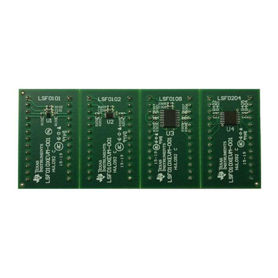
Square wave signal source Introduction The LSF010XEVM-001 is an EVM board that contains 4 LSF voltage clamp translators: 1bit, 2-bit, 4-bit, and 8 bit. These translators are bi-directional and only the LSF0204 requires a control pin. They can accept voltages up to 5.5 V on the inputs and the output will be equal to the VrefA voltage. Once the output reaches the VrefA level it can then be pulled to any other level between VrefA and 5.5 V. -
Page 3: Setup
The following are examples of how the parts can be set up: Each of these tests can be performed on any of the boards. SDLU003A – July 2014 – Revised June 2015 LSF010XEVM-001 Submit Documentation Feedback Copyright © 2014–2015, Texas Instruments Incorporated... -
Page 4: Pull-Up Resistors On Vapu And Vbpu (200Kω Integrated Within Lsf0204 Device)
This will then translate from 5 V to 2 V on Abus and then to 3.3 V on B bus. Figure 2. Pull-up Resistors on VAPU and VBPU (200kΩ integrated within LSF0204 device) LSF010XEVM-001 SDLU003A – July 2014 – Revised June 2015 Submit Documentation Feedback Copyright © 2014–2015, Texas Instruments Incorporated... -
Page 5: Open Collector Input Control Circuit
Setup www.ti.com Figure 3. Open Collector Input Control Circuit SDLU003A – July 2014 – Revised June 2015 LSF010XEVM-001 Submit Documentation Feedback Copyright © 2014–2015, Texas Instruments Incorporated... -
Page 6: Schematic
Schematic www.ti.com Schematic The circuit diagrams in Figure 4 Figure 7 show the schematics for the LSF010XEVM-001: Board Schematics and Pin Layout Figure 4. LSF0101 Schematic Table 1. LSF0101 Pin Out Pin Out Power pin (Connect high- side supply here) -
Page 7: Lsf0102 Schematic
Power pin (Connect high-side supply here) Vref_A Vref_B VAPU A side pull-up VBPU B side pull-up A1 signal B1 signal A2 signal B2 signal SDLU003A – July 2014 – Revised June 2015 LSF010XEVM-001 Submit Documentation Feedback Copyright © 2014–2015, Texas Instruments Incorporated... -
Page 8: Lsf0108 Schematic
B3 signal A4 signal B4 signal A5 signal A5 signal A6 signal A6 signal A7 signal A7 signal A8 signal A8 signal LSF010XEVM-001 SDLU003A – July 2014 – Revised June 2015 Submit Documentation Feedback Copyright © 2014–2015, Texas Instruments Incorporated... -
Page 9: Lsf0204 Schematic
VBPU B side pull-up A1 signal B1 signal A2 signal B2 signal A3 signal B3 signal A4 signal B4 signal EN pin SDLU003A – July 2014 – Revised June 2015 LSF010XEVM-001 Submit Documentation Feedback Copyright © 2014–2015, Texas Instruments Incorporated... -
Page 10: Pcb Board Layout
PCB Board Layout Figure 8 Figure 9 illustrate the PCB layout. Figure 8. PCB Layer 1 (Top Layer) Figure 9. PCB (Bottom Layer) LSF010XEVM-001 SDLU003A – July 2014 – Revised June 2015 Submit Documentation Feedback Copyright © 2014–2015, Texas Instruments Incorporated... -
Page 11: Bill Of Materials (Bom)
Changed layout pictures for top and bottom PCB layer........................• Changed BOM table. NOTE: Page numbers for previous revisions may differ from page numbers in the current version. SDLU003A – July 2014 – Revised June 2015 Revision History Submit Documentation Feedback Copyright © 2014–2015, Texas Instruments Incorporated... - Page 12 STANDARD TERMS AND CONDITIONS FOR EVALUATION MODULES Delivery: TI delivers TI evaluation boards, kits, or modules, including any accompanying demonstration software, components, or documentation (collectively, an “EVM” or “EVMs”) to the User (“User”) in accordance with the terms and conditions set forth herein. Acceptance of the EVM is expressly subject to the following terms and conditions.
- Page 13 FCC Interference Statement for Class B EVM devices NOTE: This equipment has been tested and found to comply with the limits for a Class B digital device, pursuant to part 15 of the FCC Rules. These limits are designed to provide reasonable protection against harmful interference in a residential installation.
- Page 14 【無線電波を送信する製品の開発キットをお使いになる際の注意事項】 開発キットの中には技術基準適合証明を受けて いないものがあります。 技術適合証明を受けていないもののご使用に際しては、電波法遵守のため、以下のいずれかの 措置を取っていただく必要がありますのでご注意ください。 1. 電波法施行規則第6条第1項第1号に基づく平成18年3月28日総務省告示第173号で定められた電波暗室等の試験設備でご使用 いただく。 2. 実験局の免許を取得後ご使用いただく。 3. 技術基準適合証明を取得後ご使用いただく。 なお、本製品は、上記の「ご使用にあたっての注意」を譲渡先、移転先に通知しない限り、譲渡、移転できないものとします。 上記を遵守頂けない場合は、電波法の罰則が適用される可能性があることをご留意ください。 日本テキサス・イ ンスツルメンツ株式会社 東京都新宿区西新宿6丁目24番1号 西新宿三井ビル 3.3.3 Notice for EVMs for Power Line Communication: Please see http://www.tij.co.jp/lsds/ti_ja/general/eStore/notice_02.page 電力線搬送波通信についての開発キットをお使いになる際の注意事項については、次のところをご覧くださ い。http://www.tij.co.jp/lsds/ti_ja/general/eStore/notice_02.page SPACER EVM Use Restrictions and Warnings: 4.1 EVMS ARE NOT FOR USE IN FUNCTIONAL SAFETY AND/OR SAFETY CRITICAL EVALUATIONS, INCLUDING BUT NOT LIMITED TO EVALUATIONS OF LIFE SUPPORT APPLICATIONS.
- Page 15 Notwithstanding the foregoing, any judgment may be enforced in any United States or foreign court, and TI may seek injunctive relief in any United States or foreign court. Mailing Address: Texas Instruments, Post Office Box 655303, Dallas, Texas 75265 Copyright © 2015, Texas Instruments Incorporated...
- Page 16 IMPORTANT NOTICE Texas Instruments Incorporated and its subsidiaries (TI) reserve the right to make corrections, enhancements, improvements and other changes to its semiconductor products and services per JESD46, latest issue, and to discontinue any product or service per JESD48, latest issue.
- Page 17 Mouser Electronics Authorized Distributor Click to View Pricing, Inventory, Delivery & Lifecycle Information: Texas Instruments LSF010XEVM-001...
Need help?
Do you have a question about the LSF010XEVM-001 and is the answer not in the manual?
Questions and answers