Table of Contents
Advertisement
Quick Links
ISL81802EVAL2Z
Evaluation Board
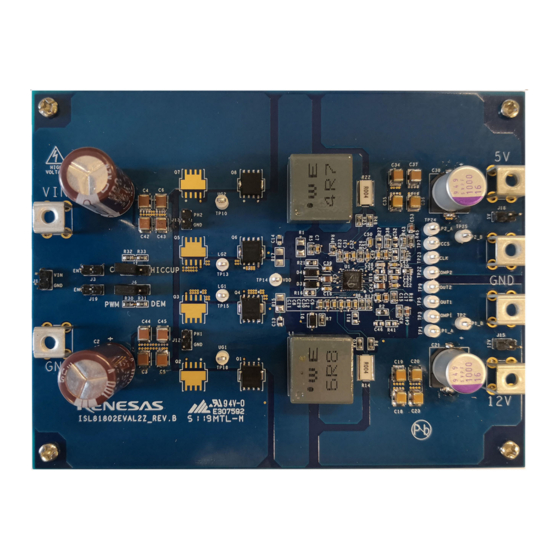
The ISL81802EVAL2Z dual-output evaluation board (shown in
voltage dual synchronous buck controller that offers external soft-start, independent enable functions, and
integrates UV/OV/OC/OT protection. A programmable switching frequency ranging from 100kHz to 1MHz helps to
optimize inductor size while the strong gate driver delivers up to 10A for each output.
Key Features
• Wide input range: 18V to 80V for 12V output, 6V to 80V for 5V output
• High light-load efficiency in pulse skipping DEM operation
• Programmable soft-start
• Optional DEM/PWM operation
• Optional CC/HICCUP OCP protection
• Supports pre-bias output with soft-start
• PGOOD indicator
• OVP, OTP, and UVP protection
• Back biased from output to improve efficiency
Specifications
The ISL81802EVAL2Z dual-output evaluation board is designed for high current applications. The current rating
of the ISL81802EVAL2Z is limited by the FETs and inductor selected. The ISL81802EVAL2Z electrical ratings are
shown in
Table
1.
Table 1.
ISL81802EVAL2Z Electrical Ratings
Parameter
Input Voltage
Switching Frequency
Output Voltage 1
Output Current 1
Output Voltage 2
Output Current 2
OCP Set Point
Ordering Information
Part Number
ISL81802EVAL2Z
Related Literature
For a full list of related documents, visit our website:
•
ISL81802
device page
R16UH0003EU0100 Rev.1.00
Aug.24.20
18V to 80V (6V to 80V for 5V output)
200kHz
12V
10A
5V
10A
Minimum 12.6A each output at ambient room temperature
High Voltage Dual Buck Controller Evaluation Board
Figure
4) features the ISL81802, an 80V high
Rating
Description
User Manual
Page 1 of 25
Advertisement
Table of Contents

Related Manuals for Renesas ISL81802EVAL2Z


Summary of Contents for Renesas ISL81802EVAL2Z
- Page 1 • Back biased from output to improve efficiency Specifications The ISL81802EVAL2Z dual-output evaluation board is designed for high current applications. The current rating of the ISL81802EVAL2Z is limited by the FETs and inductor selected. The ISL81802EVAL2Z electrical ratings are shown in Table Table 1.
- Page 2 ISL81802EVAL2Z 6V-80V 5V/10A 12V/10A Figure 1. ISL81802EVAL2Z Block Diagram R16UH0003EU0100 Rev.1.00 Page 2 of 25 Aug.24.20...
-
Page 3: Functional Description
1. Functional Description Functional Description The ISL81802EVAL2Z is the same test board used by Renesas application engineers and IC designers to evaluate the performance of the ISL81802 TQFN IC. The board provides an easy and complete evaluation of all the IC and board functions. - Page 4 ISL81802EVAL2Z 1. Functional Description Quick Test Guide 1. Jumper J6 provides the option to select PWM or DEM. Jumper J7 provides the option to select a constant current limit or HICCUP. See Table 2 for the operating options. Ensure that the circuit is correctly connected to the supply and electronic loads before applying any power.
-
Page 5: Pcb Layout Guidelines
MOSFETs. 2. If signal components and the IC are placed separately from the power train, Renesas recommends using full ground planes in the internal layers with shared SGND and PGND to simplify the layout design. Otherwise, use separate ground planes for the power ground and the small signal ground. - Page 6 ISL81802EVAL2Z 2. PCB Layout Guidelines ISL81802EVAL2Z Evaluation Board Figure 4. ISL81802EVAL2Z Evaluation Board, Top View Figure 5. ISL81802EVAL2Z Evaluation Board, Bottom View R16UH0003EU0100 Rev.1.00 Page 6 of 25 Aug.24.20...
- Page 7 ISL81802EVAL2Z Circuit Schematic 15V-80V Figure 6. Schematic...
-
Page 8: Bill Of Materials
ISL81802EVAL2Z 2. PCB Layout Guidelines Bill of Materials Reference Designator Description Manufacturer Manufacturer Part PWB-PCB, ISL81802EVAL1Z, REVB, ROHS Multilayer ISL81802EVAL1ZREVBPCB PCB Technology C1, C2 CAP, RADIAL, 12.5x26.5, 220μF, 100V, United Chemi-Con EKZN101ELL221MK25S 20%, ALUM.ELEC., 5mm, ROHS C3, C4, C5, C6, C42, C43, CAP-AEC-Q200, SMD, 1210, 4.7μF, 100V,... - Page 9 ISL81802EVAL2Z 2. PCB Layout Guidelines Reference Designator Description Manufacturer Manufacturer Part RES SMD 430kΩ 1% 1/4W 1206 Panasonic ERJ-8ENF4303V R2, R5, R43 RES SMD 48.7kΩ 1% 1/10W 0603 Yageo RC0603FR-0748K7L R3, R45 RES SMD 20Ω 1% 1/10W 0603 Yageo RC0603FR-0720RL R6, R10, R25, R48 RES SMD 1Ω...
-
Page 10: Board Layout
ISL81802EVAL2Z 2. PCB Layout Guidelines Board Layout Figure 7. Silkscreen Top Figure 8. Top Layer R16UH0003EU0100 Rev.1.00 Page 10 of 25 Aug.24.20... - Page 11 ISL81802EVAL2Z 2. PCB Layout Guidelines Figure 9. Second Layer (Solid Ground) Figure 10. Third Layer R16UH0003EU0100 Rev.1.00 Page 11 of 25 Aug.24.20...
- Page 12 ISL81802EVAL2Z 2. PCB Layout Guidelines Figure 11. Bottom Layer Figure 12. Silkscreen Bottom R16UH0003EU0100 Rev.1.00 Page 12 of 25 Aug.24.20...
-
Page 13: Design Example
ISL81802EVAL2Z 3. Design Example Design Example Design Requirements Parameter Rating Input Voltage 18V to 80V for 12V output 6V to 80V for 5V output Switching Frequency 200kHz Output Voltage 1 Output Current 1 Output Voltage 2 Output Current 2 OCP Set Point 12.6A for each output... - Page 14 ISL81802EVAL2Z 3. Design Example UVLO Setting The ISL81802 has input UVLO protection. When the voltage on the EN/UVLO pin reaches 1.8V, the PWM modulator is enabled. Accurate UVLO feature can be implemented by feeding the V into the EN/UVLO pin using...
-
Page 15: Inductor Selection
ISL81802EVAL2Z 3. Design Example Inductor Selection The inductor value determines the ripple current of the converter. The ripple voltage is a function of the ripple current and the output capacitor(s) ESR. Assume the ripple current ratio is 80% of the inductor average current at the maximum input voltage and the full output load condition. - Page 16 RMSMAX OUTMAX Renesas recommends using a mix of input bypass capacitors to control the voltage ripple across the MOSFETs. Use ceramic capacitors for the high frequency decoupling and bulk capacitors to supply the RMS current. Two 220µF electrolytic capacitors with 2.2A rating current and eight 4.7µF ceramic capacitors are used to share the 5A RMS input current on this board.
- Page 17 A resistor less than 30kΩ sets the converter to forced PWM mode, while a resistor higher than 30kΩ sets the converter to DE mode. Considering the tolerance in all temperature ranges, Renesas recommends using 15kΩ to set to Forced PWM node and 51kΩ to set to DE mode.
- Page 18 ISL81802EVAL2Z 3. Design Example 3.16 Feedback Loop Compensation To adapt the different applications, the controller is designed with an externally compensation network. Figure 13 shows the peak current mode buck converter circuit. Slope Clock (0.8V) Figure 13. Peak Current Mode Buck Converter Circuit...
- Page 19 = 1/2πR • The first zero is at the frequency of f = 1/2πR • The second zero is at the frequency of f = 1/2πR To achieve ideal compensation, Renesas recommends making f and f as shown in z(esr) Figure...
- Page 20 ISL81802EVAL2Z 3. Design Example The close-loop transfer function is then simplified to Equation ------------------ - 1 z esr s ------------------ - ------------------------------------------------- - ------------------------------------------------------------------ - ------------------ - ------------------ (EQ.
- Page 21 ISL81802EVAL2Z 3. Design Example If R ) = 48.7k, R ) = 3.48k, R ) = 22k, C (C46) = 150pF, C ) can be calculated using Equation 1.2 ------------------ - ------------------- - ---------------------------------------- - --------------------------------------------------------- - (EQ. 45) 25.1nF...
-
Page 22: Typical Performance Curves
ISL81802EVAL2Z 4. Typical Performance Curves Typical Performance Curves = 48V, T = 25°C, unless otherwise noted. Vin = 8V Vin = 12V Vin = 18V Vin = 24V Vin = 24V Vin = 36V Vin = 36V Vin = 48V... - Page 23 ISL81802EVAL2Z 4. Typical Performance Curves = 48V, T = 25°C, unless otherwise noted. (Continued) Phase 1 50V/Div 200mV/Div OUT1 100mV/Div OUT2 Phase 2 50V/Div 10A/Div 10A/Div 10A/Div 10A/Div 2µs/Div 2ms/Div Figure 21. V = 80V, V = 12V, V = 5V, I = 10A, Figure 22.
- Page 24 ISL81802EVAL2Z 4. Typical Performance Curves = 48V, T = 25°C, unless otherwise noted. (Continued) 200mV/Div OUT1 10V/Div OUT1 200mV/Div OUT2 10V/Div OUT2 10A/Div 10A/Div 10A/Div 10A/Div 10ms/Div 4ms/Div Figure 27. Start-Up Waveform, V = 80V, V = 12V, Figure 28. Burst Mode Waveforms, V...
-
Page 25: Revision History
ISL81802EVAL2Z 5. Revision History Revision History Rev. Date Description 1.00 Aug.24.20 Initial release R16UH0003EU0100 Rev.1.00 Page 25 of 25 Aug.24.20... - Page 26 Renesas' products are provided only subject to Renesas' Terms and Conditions of Sale or other applicable terms agreed to in writing. No use of any Renesas resources expands or otherwise alters any applicable warranties or warranty disclaimers for these products.
Need help?
Do you have a question about the ISL81802EVAL2Z and is the answer not in the manual?
Questions and answers