
Subscribe to Our Youtube Channel
Related Manuals for Texas Instruments SWIFT TPS54680EVM-228


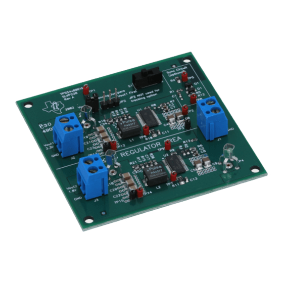
Summary of Contents for Texas Instruments SWIFT TPS54680EVM-228
- Page 1 TPS54680EVM−228 6−Amp, TPS54880EVM−228 8−Amp, SWIFTE Regulator Evaluation Module User’s Guide November 2002 PMP EVMs SLVU077...
- Page 2 IMPORTANT NOTICE Texas Instruments Incorporated and its subsidiaries (TI) reserve the right to make corrections, modifications, enhancements, improvements, and other changes to its products and services at any time and to discontinue any product or service without notice. Customers should obtain the latest relevant information before placing orders and should verify that such information is current and complete.
- Page 3 EVM IMPORTANT NOTICE Texas Instruments (TI) provides the enclosed product(s) under the following conditions: This evaluation kit being sold by TI is intended for use for ENGINEERING DEVELOPMENT OR EVALUATION PURPOSES ONLY and is not considered by TI to be fit for commercial use. As such, the goods being provided may not be complete in terms of required design-, marketing-, and/or manufacturing-related protective considerations, including product safety measures typically found in the end product incorporating the goods.
- Page 4 EVM schematic located in the EVM User’s Guide. When placing measurement probes near these devices during operation, please be aware that these devices may be very warm to the touch. Mailing Address: Texas Instruments Post Office Box 655303 Dallas, Texas 75265 Copyright 2002, Texas Instruments Incorporated...
- Page 5 Operation of this equipment in other en- vironments may cause interference with radio communications, in which case the user at his own expense will be required to take whatever measures may be required to correct this interference. Trademarks SWIFT and PowerPAD are trademarks of Texas Instruments.
-
Page 7: Table Of Contents
Contents Contents Introduction ..............Background . - Page 8 Contents Figures Different Power Sequencing Technique Selection ....... . . Frequency Trimming Resistor Selection Graph .
- Page 9 Contents Tables Input Voltage and Output Current Summary ........TPS54680EVM-228 Performance Specification Summary .
- Page 10 Contents...
-
Page 11: Introduction
Chapter 1 Introduction This chapter contains background information for the TPS54680 and TPS54880 as well as performance specifications and support documentation for the TPS54680EVM-228, TPS54880EVM-228 evaluation modules (SLVP228). Different types of power sequencing and implementation using TPS54x80 tracking regulators are described. Topic Page Background... -
Page 12: Background
Background 1.1 Background The SWIFT family TPS54680 and TPS54880 tracking dc/dc converters are designed to provide accurate power sequencing in applications where two or more voltages are required for a load. These types of applications include core and I/O power supplies for microprosessors, DSPs and FPGAs. Typically, some specific relation between the core and I/O supply voltages has to be provided during the power-up and power-down sequences. -
Page 13: Input Voltage And Output Current Summary
Background The switching frequency is set at a nominal 700 kHz, allowing the use of a small footprint 0.65 µH output inductor. The MOSFETs of the SWIFT regulators are incorporated inside the package. This eliminates the need for external MOSFETs and their associated drivers. The low drain-to-source on resistance of the MOSFETs gives the SWIFT... -
Page 14: Performance Specification Summary
Performance Specification Summary 1.2 Performance Specification Summary A summary of the TPS54x80EVM-228 performance specifications is provided in Table 1-2 and Table 1-3. These data relate only to core voltage outputs of the TPS54680 and TPS54880. The performance specification summaries for the TPS54610 and TPS54810 can be found in the related User’s Guide, TI literature number SLVU071. -
Page 15: Tps54880Evm-228 Performance Specification Summary
Performance Specification Summary Table 1-3. TPS54880EVM-228 Performance Specification Summary Specification Test Conditions Units † Input voltage range Output voltage set point range Output current range Line regulation = 0 A-8 A -0.2% 0.2% Load regulation = 5 V -0.2% 0.2% I = 1.5 A to 4.5 A, t(rise) = 1 µs, = 1.5 A to 4.5 A, t(rise) = 1 µs, µs... -
Page 16: Tracking Regulator And Power Sequencing
Tracking Regulator and Power Sequencing 1.3 Tracking Regulator and Power Sequencing To avoid potential problems with the processor and system ICs, designers can apply three general techniques for power-up sequencing: sequential, ratiometric, or simultaneous. Sequential power up, as the name implies, powers up the two rails one after the other. -
Page 17: Modifications
Modifications 1.4 Modifications The TPS54x80EVM-228 evaluation module is designed to demonstrate the small size using ceramic capacitors that can be attained when designing with the TPS54x80. Meanwhile, the solution is not limited only to these particular output voltages and switching frequency. The following paragraphs describe what kind of modifications can be done to meet different application requirements. -
Page 18: Frequency Trimming Resistor Selection Graph
Modifications Figure 1-2. Frequency Trimming Resistor Selection Graph R - Resistance - kΩ... -
Page 19: Test Setup And Results
Chapter 2 Test Setup and Results This chapter describes how to properly connect, setup, and use the TPS54x80EVM-228 evaluation module. The chapter also includes test results typical for the TPS54x80EVM-228 and covers efficiency, overall power dis- sipation, output voltage regulation, load transients, loop response, output rip- ple, input ripple, and different ways of power sequencing and tracking during power up and power down. -
Page 20: Input/Output Connections
Input/Output Connections 2.1 Input/Output Connections The TPS54x80EVM-228 has the following input/output connections: 5-V input, 5-V input return, 3.3-V output, 3.3-V output return, 1.8-V output and 1.8-V output return. A diagram showing the connection points is shown in Figure 2-1. A power supply capable of supplying 15 A should be connected to J1 through a pair of 16 AWG wires. -
Page 21: Connection Diagram
Input/Output Connections Figure 2-1. Connection Diagram Oscilloscope Power Supply 4 to 6 V, 15A Load 0 - 9A Voltmeter 1 Optional Input Capacitor Load 0 - 9A Voltmeter 2 Test Setup and Results... -
Page 22: Power Sequencing Test
Power Sequencing Test 2.2 Power Sequencing Test The TPS54x80 regulators provide different modes for power-up and power-down sequencing of the core and I/O voltages. By selecting the different ratios for the resistor divider R3/R6 (Figure 4-1), the slope of the core voltage during power up and down can be set equal to, higher than, or lower than the slope of I/O voltage. -
Page 23: Powering Down With Tracking
Power Sequencing Test rate of about 75 V/ms, there is less than 0.3-V difference between the core voltage and I/O voltage. This difference and some delay are caused by the response time of the feedback loop of tracking regulator. For most applications the I/O voltage falls much slower and the difference between core and I/O voltage becomes negligible. -
Page 24: Powering Up With Ratiometric Sequencing
Power Sequencing Test Figure 2-4. Powering Up With Ratiometric Sequencing Figure 2-5. Powering Down With Ratiometric Sequencing... -
Page 25: Powering Up With Core Voltage Rising First
Power Sequencing Test If jumper JP2 is set so that R2 is connected in parallel to R3, the core voltage rises first during power up, i.e. prior to the I/O voltage rise, and falls second during power down. The waveforms with this type of sequencing are shown in Figure 2-6 and Figure 2-7. -
Page 26: Efficiency
Efficiency 2.3 Efficiency The TPS54x80EVM-228 efficiency depends on output voltage, even though the power losses are roughly the same for any output voltage. Efficiency also depends on input voltage. For the output current below 3 A, the efficiency is higher at 3.3-V input voltage because of lower switching losses. For the output current above 3 A, the efficiency is better at 5-V input voltage because of lower drain-to-source resistance of integrated FETs driven by higher gate voltage. -
Page 27: Power Dissipation
Power Dissipation 2.4 Power Dissipation The low junction-to-case thermal resistance of the PWP package with PowerPad, along with a good board layout, allows the TPS54x80EVM-228 to provide full rated load current while maintaining safe junction temperatures. The total board losses at 25°C are shown in Figure 2-9. The input voltage is 5 V. -
Page 28: Output Voltage Regulations
Output Voltage Regulations 2.5 Output Voltage Regulations The output voltage load regulation of the TPS54x80EVM-228 is shown in Figure 2-10, while the output voltage line regulation is shown in Figure 2-11. Measurements are given for an ambient temperature of 25°C. Figure 2-10. -
Page 29: Load Transients
Load Transients 2.6 Load Transients TPS54x80EVM-228 response to load transients is shown in Figure 2-12 and Figure 2-13. The current step is from 1.5 A to 4.5 A with the slew rate 5A/µs. For these measurements: Ch.2: Output voltage 100 mV/div. Ch.4: Load current 2 A/div. -
Page 30: Loop Characteristics
Loop Characteristics 2.7 Loop Characteristics The TPS54x80EVM-228 loop response characteristics are shown in Figure 2-14 and Figure 2-15. Gain and phase plots are shown at 3.3 V for TPS54680 and at 5 V for TPS54680 and TPS54880 regulators. Figure 2-14. Measured Loop Response, TPS54680, V = 3.3 V, V = 1.8 V TPS54680-228... -
Page 31: Output And Input Voltage Ripple And Main Switching Waveforms
Output and Input Voltage Ripple and Main Switching Waveforms 2.8 Output and Input Voltage Ripple and Main Switching Waveforms The TPS54x80EVM-228 evaluation module output and input voltage ripple and main switching waveforms at V = 3.3 V, V = 1.8 V, I = 6 A and Fs = 700 kHz are shown in Figure 2-16. -
Page 32: Input And Output Voltage Ripple And Main Switching Waveform At V I = 5 V
Output and Input Voltage Ripple and Main Switching Waveforms Figure 2-17. Input and Output Voltage Ripple and Main Switching Waveform at V = 5 V 2-14... -
Page 33: Board Layout
Chapter 3 Board Layout This chapter provides a description of the TPS54x80EVM-228 board layout and layer illustrations. Topic Page Board Layout ..........Board Layout... -
Page 34: Layout
Layout 3.1 Layout The board layout for the TPS54x80EVM-228 is shown in Figure 3-1 through Figure 3-4. The top side layer of the TPS54x80EVM-228 is laid out in a man- ner typical of a user application. The top and bottom layers are 1.5 oz. copper, while the two internal layers are 0.5 oz. -
Page 35: Top Side Layout
Layout Figure 3-2. Top SIde Layout Figure 3-3. Internal Layer 2 Layout Board Layout... -
Page 36: Internal Layer 3 Layout
Layout Figure 3-4. Internal Layer 3 Layout Figure 3-5. Bottom Side Layout (looking from top side) -
Page 37: Schematic And Bill Of Materials
Chapter 4 Schematic and Bill of Materials The TPS54x80EVM-228 schematic and bill of materials are presented in this chapter. Topic Page Schematic ........... . Bill of Materials . -
Page 38: Schematic
Schematic 4.1 Schematic The schematic for the TPS54x80EVM-228 is shown in Figure 4-1. Figure 4-1. TPS54x80EVM-228 Schematic... -
Page 39: Bill Of Materials
Bill of Materials 4.2 Bill of Materials The bill of materials for the TPS54x80EVM-228 is given by Table 4-1. Table 4-1. TPS54x80EVM-228 Bill of Materials Count Ref Des Description SIze Part Number Capacitor, ceramic, 100 pF, 50 V, Murata GRM1885C1H101JA01 C0G, 5% C11, C13 Capacitor, ceramic, 3300 pF,... - Page 40 Bill of Materials Count Ref Des Description SIze Part Number TP1, TP2, TP5, Test point, red, 1 mm 0.038″ Farnell 240-345 TP6, TP7, TP8, TP9, TP12, TP14 TP3, TP13, TP15 Test point, black, 1 mm 0.038″ Farnell 240-333 TP4, TP10, TP11 Adaptor, 3,5 mm probe clip (or 72900 Tektronix...
-
Page 41: A Out Of Phase Synchronization Of I/O And Core Swift Family Regulators
Appendix A Out of Phase Synchronization of I/O and Core SWIFTE Family Regulators This chapter provides additional information about the TPS54x80EVM-228. If the core and I/O voltages are provided by the two dc/dc regulators running at a slightly different frequencies with the same input power supply, their input voltage ripple always includes a low frequency harmonic. -
Page 42: Core Regulator (Ch4) And I/O Regulator (Ch1
Figure A-2. Input Voltage Ripple (Ch.2),Sync Signal (Ch.3) and Switching Waveforms of Core Regulator (Ch.4) and I/O Regulator (Ch.1) In many cases, this low frequency harmonic does not affect on overall perfor- mance of system. However, by synchronizing both switching regulators out of phase, it is possible to avoid the beating effect and to save some input capaci- tors because of ripple cancellation effect. -
Page 43: Phase Core Regulator (Ch4) And I/O Regulator (Ch1
Figure A-3. Input Voltage Ripple (Ch.2)and Switching Waveforms of Synchronized Out of Phase Core Regulator (Ch.4) and I/O Regulator (Ch.1) Figure A-4. Input Voltage Ripple (Ch.2 and Switching Waveforms of Nonsynchronized Core Regulator (Ch.4) and I/O Regulator (Ch.1) It can be seen that the input voltage ripple of synchronized regulators is 100 mV peak-to-peak, while the input voltage ripple of nonsynchronized regulators is 150 mV peak-to-peak.
Need help?
Do you have a question about the SWIFT TPS54680EVM-228 and is the answer not in the manual?
Questions and answers